Contents
- I. Module Introduction
- II. Introduction to Major Chips
- 2.1 Chip Overview
- 2.2 Pin Definition
- 2.3 Functional Block Diagram
- 2.4 Performance Parameters
- 2.5 Reference Circuit
- 2.6 Chip Configuration
- 2.7 Communication Interfaces and Related Protocols
- 2.8 PCB Routing Precautions
- III. Circuit Engineering
- 3.1 Circuit Source Engineering
- 3.2 Module Usage Instructions
- 3.3 Application Experiment
- 4. Drivers
- 5. BOM & Recommended Alternative Parts
- VI. Revision History
- VII. Relevant Materials
- 7.1 Chip Datasheet
- 7.2 PCB Silkscreen Specific Icons
I. Module Introduction
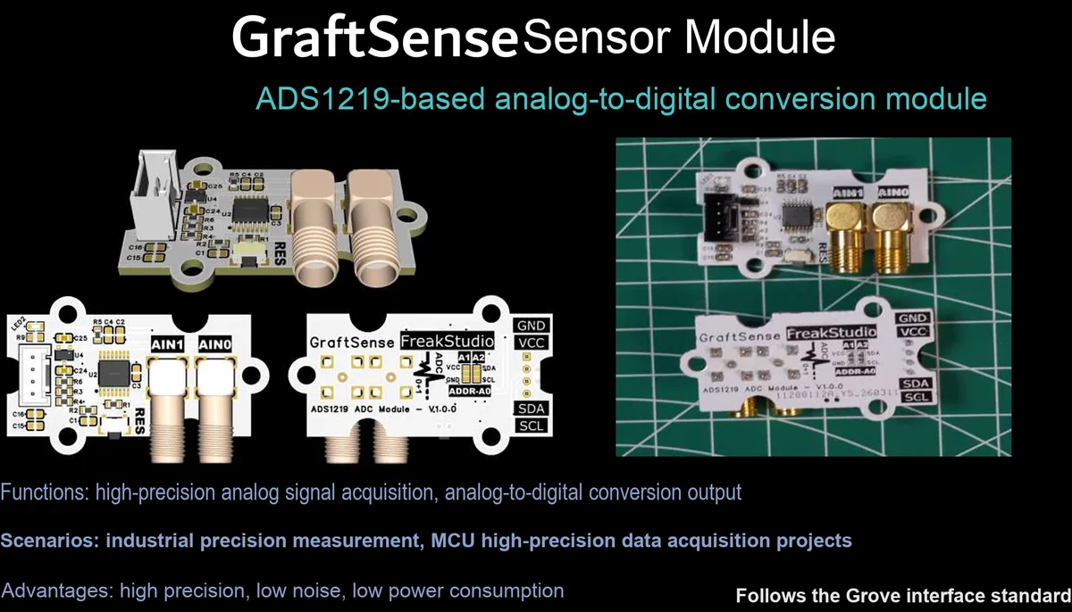
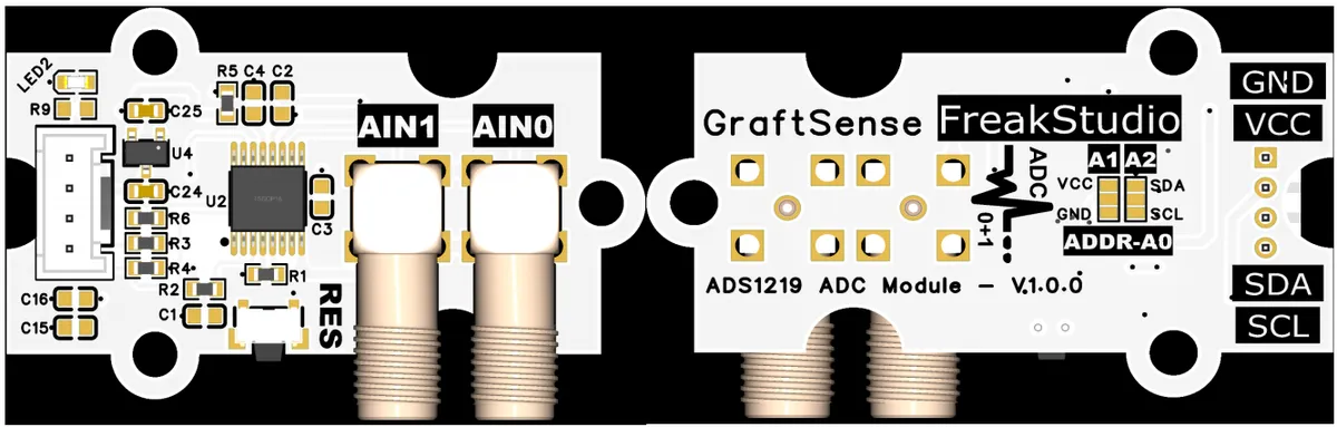
ADS1219-Based Analog-to-Digital Conversion Module which adopts a 24-bit ΔΣ type ADS1219IPWR chip, communicates with MCU via the I²C interface, supports 4 configurable I²C addresses, and is equipped with two SMA analog input interfaces and a 5V-to-3.3V power supply circuit. With separate analog/digital power supplies and decoupling capacitors for noise suppression, this module can realize high-precision analog signal acquisition, and is suitable for low-noise Data Acquisition scenarios such as industrial sensing and precision measurement.
II. Introduction to Major Chips
ADS1219 is a 24-bit ΔΣ high-precision ADC that features an I²C interface, supports programmable gain and data rates, and integrates a low-noise amplifier and a reference voltage. It is suitable for low-noise analog signal acquisition scenarios such as precision sensing and industrial measurement.
2.1 Chip Overview
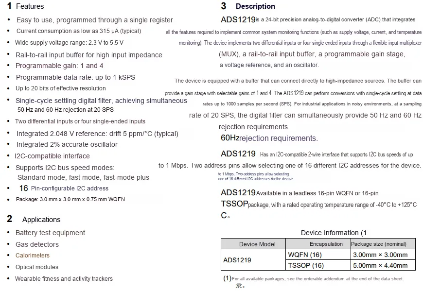
ADS1219 is a 24-bit precision delta-sigma analog-to-digital converter that requires only a single register for programming, operates with a supply voltage range of 2.3V to 5.5V, and features a typical current consumption as low as 315μA; it offers 2 differential / 4 single-ended inputs, adopts an I²C-compatible interface (up to 1Mbps), supports 16 configurable I²C addresses, and has an operating temperature range of -40°C to + 125°C, making it suitable for high-precision, low-noise acquisition scenarios such as battery testing, gas detection, and calorimeters.
2.2 Pin Definition
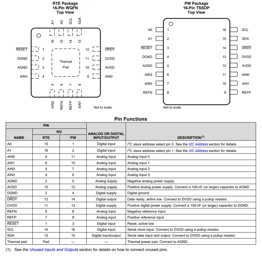
ADS1219 is available in two packages: WQFN and TSSOP, both with 16 pins, and the pins are mainly categorized as follows:
- Address and Communication:
A0/A1areI²Caddress selection pins,SCL/SDAareI²Ccommunication pins, andDRDYis a data ready output pin; - Analog Inputs:
AIN0~AIN3are analog input channels that can be configured as differential or single-ended inputs;REFN/REFPserve as reference voltage inputs. - Power Supply and Ground:
AVDD/AGNDrefer to the analog power supply and ground,DVDD/DGNDrefer to the digital power supply and ground, which require separate decoupling; - Control:
RESETis the reset pin, and the additional thermal pad shall be connected to the analog groundAGND.
2.3 Functional Block Diagram
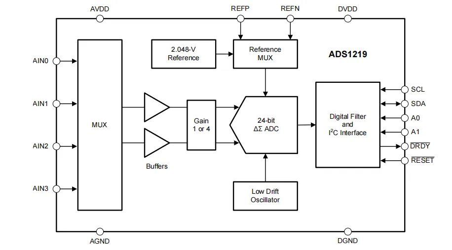
ADS1219 has a functional block diagram centered around a 24-bit ΔΣ ADC. It selects analog inputs via a multiplexer (MUX), amplifies the signals through a rail-to-rail buffer and a programmable gain stage, performs analog-to-digital conversion driven by the built-in 2.048V reference voltage and low-drift oscillator, and finally outputs data through a digital filter and the I²C interface. It also integrates control modules for power supply, reset, and address configuration.
2.4 Performance Parameters
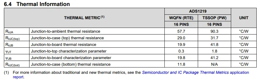
ADS1219 has the following absolute maximum ratings: the analog/digital power supply voltage range is -0.3V to 7V, the analog/digital input voltage range is (corresponding to ground) -0.3V to (power supply) + 0.3V, the continuous input current of each pin is ±10mA, and the upper limit of junction temperature and storage temperature is 150°C;ESD protection capability reaches HBM ±2000V and CDM ±750V. Exceeding these limits will cause permanent damage to the device.
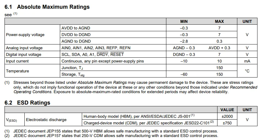
ADS1219 recommended operating conditions are as follows: analog/digital supply voltage range: 2.3V to 5.5V, voltage difference between analog ground and digital ground: -0.1V to 0.1V; analog input voltage range is AGND -0.1V to AVDD + 0.1V, differential input voltage does not exceed ± VREF / gain; reference voltage differential input range: 0.75V to 2.5V; digital input voltage is compatible with DVDD level; operating ambient temperature range: -40°C to + 125°C.
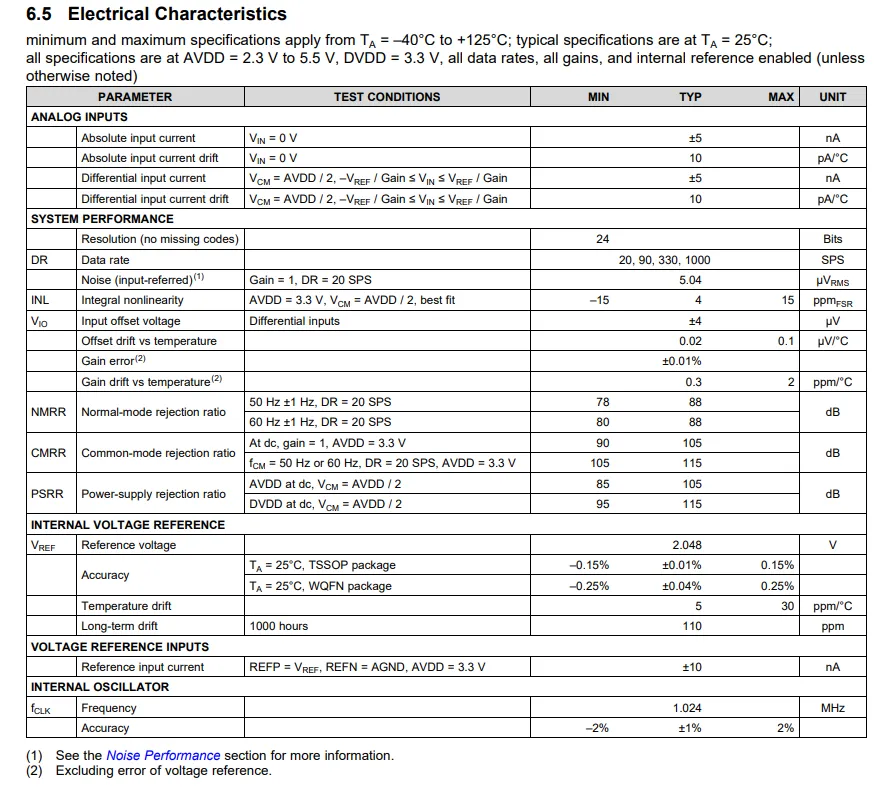
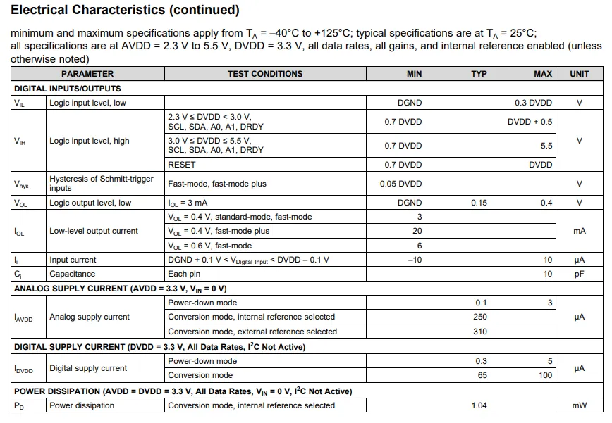
ADS1219 is a 24-bit high-precision ADC, featuring a data rate of 20 to 1000 SPS, a programmable gain of 1/4, a typical input noise of 5.04 μVRMS, and the capability to simultaneously suppress 50/60 Hz power line interference at 20 SPS;It features a built-in 2.048V reference voltage (typical drift: 5ppm/°C). In conversion mode, the typical current consumption of its analog and digital power supplies are 250μA and 65μA respectively, with an overall power consumption of only 1.04mW. Equipped with high common-mode rejection ratio and power supply rejection ratio, it is ideal for low-noise precision acquisition scenarios.
2.5 Reference Circuit
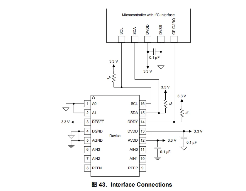
This is the ADS1219 and microcontroller I²C interface reference circuit: both analog and digital power supplies are 3.3V with decoupling capacitors, SCL / SDA / DRDY pins are connected to 3.3V pull-up resistors, A0 / A1 are grounded to configure the I²C address, RESET is connected to high level, the analog ground and digital ground are common grounded, which can realize high-precision ADC acquisition.
2.6 Chip Configuration
None.
2.7 Communication Interfaces and Related Protocols
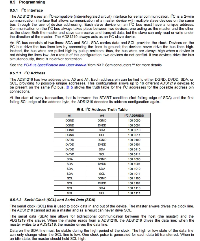
ADS1219 uses I ² C compatible interface as slave communication, through SCL and SDA dual-wire transmission, the bus needs external pull-up resistor; it has A0 / A1 two address pins, can be connected to DGND , DVDD , SDA or SCL , providing 16 configurable I ² C addresses , supporting up to 16 devices to work with the bus; SCL is driven by the host, SDA is a bidirectional transmission line, data needs to be in SCL Stable during high levels, communication follows standard I ² C timing specifications.
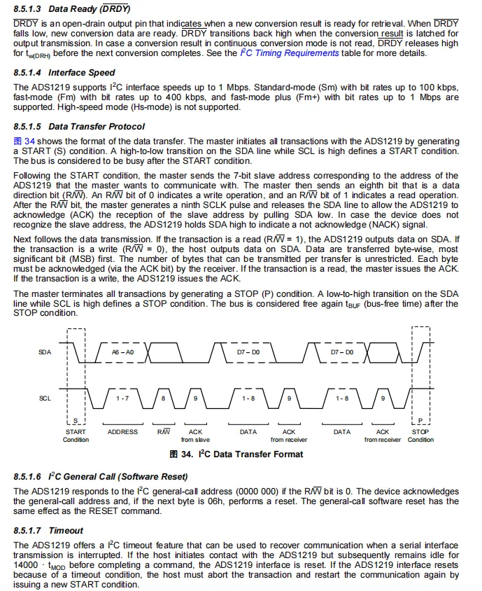
ADS1219 's I²C interface supports a maximum communication rate of 1 Mbps, and uses the open-drain output DRDY pin to indicate that conversion data is ready; data transmission complies with the standard I²C protocol, where the master initiates START / STOP conditions, first sends a 7-bit slave address and a read/write bit, and transmits data after an ACK response. It also supports general call software reset and timeout auto-reset functions to ensure stable and reliable communication.
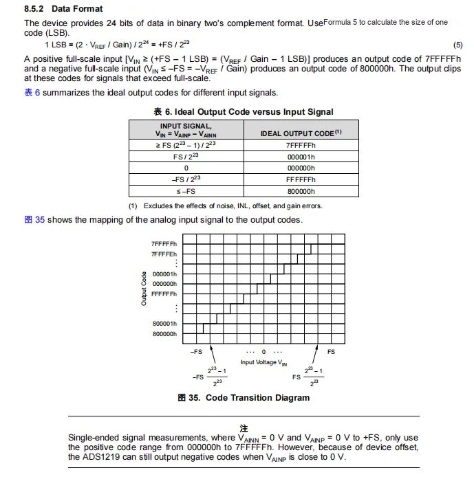
ADS1219 outputs 24-bit two's complement data. The voltage corresponding to 1 LSB is (2⋅ VREF / Gain)/2^24; the positive full-scale input corresponds to the code 7FFFFFh, and the negative full-scale corresponds to 800000h. For single-ended measurement, only the positive code range from 000000h to 7FFFFFh is used, and any out-of-range input will be clamped to the corresponding extreme value code.
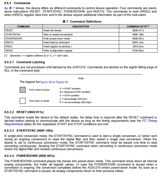
ADS1219 provides 6 types of I²C control commands, including RESET (reset), START / SYNC (start/synchronous conversion), POWERDOWN (enter power-down mode), RDATA (read data), RREG (read register), and WREG (write register). The commands are latched and take effect on the 8th falling edge of SCL in the command byte; among them, standalone commands require no additional data, while register read/write commands need to be accompanied by address and data fields, enabling device reset, conversion control, power consumption management and parameter configuration.
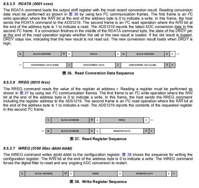
ADS1219 's RDATA / RREG / WREG commands all require two I²C frames for interaction:
RDATA: First write the command frame, then read the data frame to acquire the latest 24-bit conversion result;DRDYlevel indicates whether the data is new or old.RREG: First write the instruction frame with the register address, then read the content of the corresponding register;WREG: Single-frame write completes the configuration register write, which will force a reset of the digital filter and restart the conversion.
The entire instruction process strictly complies with I²C read and write timings, and communication reliability is guaranteed via ACK responses.
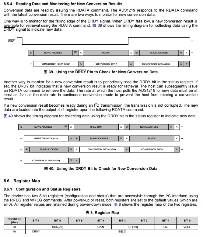
ADS1219 provides two new data monitoring methods: one is triggered by the DRDY pin level falling edge reading, and the other is judged by the DRDY bit polling in the status register; the converted data needs to be read by the RDATA instruction, and the device only contains two 8-bit registers (configuration register 0x0h , status register 0x1h ), and the default is all 0 after power-on/reset. The register value remains unchanged in power-down mode, and the configuration can be accessed through the RREG / WREG instruction.
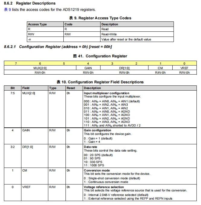
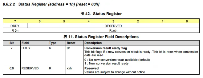
- Configuration Register (
0x0h): Readable and writable, with a power-on default value of0x00. It contains fields such as multiplexer selection (MUX[2:0]), gain configuration (GAIN), data rate (DR[1:0]), conversion mode (CM) and reference source selection (VREF), which are used to set the input channel, amplification factor, sampling rate, single/continuous conversion mode and reference voltage source. - Status Register (
0x1h): Read-only, default value at power-on is0x00; only the highest bitDRDYis a valid bit, which is used to indicate whether a new conversion result is ready, and the remaining bits are reserved bits.
The entire register set features a streamlined design, and full-function configuration and status query can be completed simply via RREG / WREG instructions.
2.8 PCB Routing Precautions
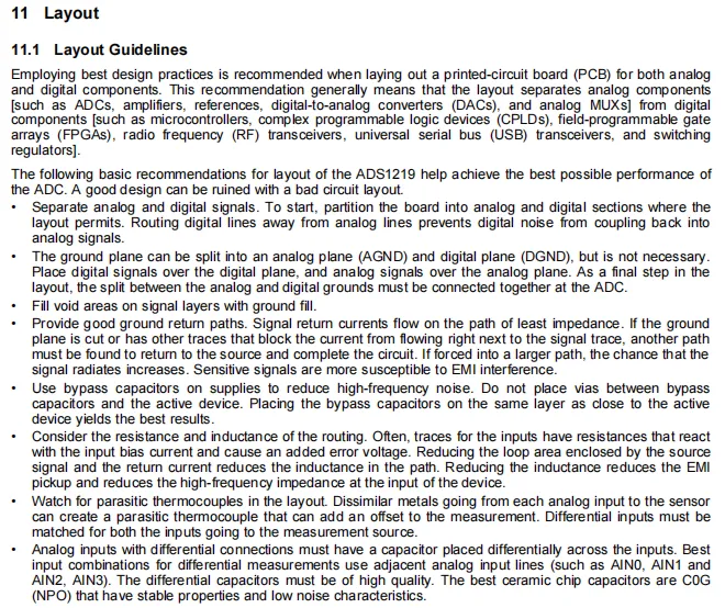
ADS1219 PCB layout core principles are analog-digital separation, low-noise grounding and decoupling:
- Divide the board into an analog area and a digital area, and keep digital signals away from analog signals to avoid noise crosstalk;
- The ground plane can be divided into
AGNDandDGND, which are eventually connected at a single point at theADCto ensure a proper signal return path; - Place decoupling capacitors close to the power pins to reduce high-frequency noise;
- Reduce the signal loop area to lower
EMIpickup and avoid measurement offset caused by parasitic thermocouples; - Differential inputs require matched routing, and a high-quality differential capacitor should be connected across the input terminals to ensure measurement accuracy.
This layout guideline can maximize the ADS1219 high-precision and low-noise performance.
III. Circuit Engineering
3.1 Circuit Source Engineering
To obtain the circuit source project, please follow the official account [Freak Embedded].
3.2 Module Usage Instructions
The schematic diagram of this module is shown below:
SCH_ADC Module Based on ADS1219-V1.0.0_2026-03-24.pdf 2.4 MB
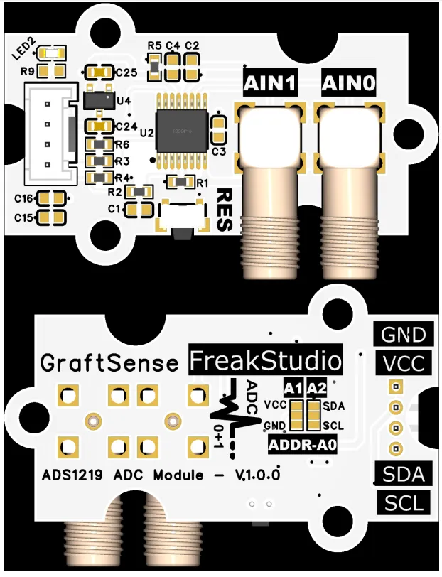
This module provides an I²C communication interface: it supports a maximum high-speed I²C communication rate of 1Mbps, and 4 types of ADDR - A0, A1, A2 short-circuit points allow flexible configuration of I²C addresses, is compatible with 3.3V level, can stably realize the reading of 24-bit high-precision ADC data and register configuration operations, is suitable for low-noise Data Acquisition scenarios such as industrial sensing and precision measurement, and provides the system with reliable high-precision analog signal acquisition and interaction capabilities.
Two SMA interfaces are adopted for signal input, which can be connected to the signal generator end via SMA related adapter cables.
3.3 Application Experiment
Here, we use the GraftPort-RP2040 development board for testing, and the ADS1219-based analog-to-digital conversion module uses the I2C interface to communicate with the main controller.
Here, we first use the HY2.0-4P cable to connect the module to the GraftPort-RP2040 development board's I2C0 interface:
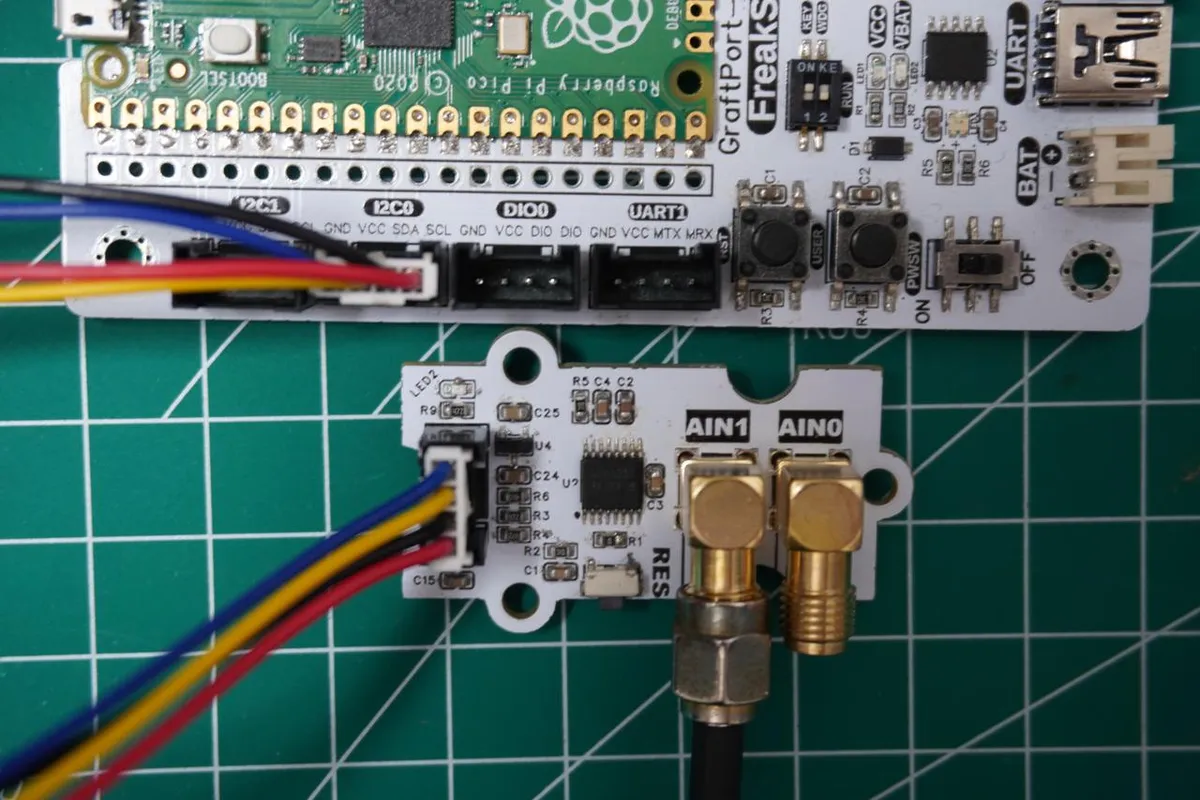
The module connections are shown in the following table:
Development Board Pins | Module Pins | Description |
Pin 4 |
|
|
Pin 5 |
|
|
Then use an SMA adapter cable to connect to the signal generator, and configure the output waveform settings of the signal generator:
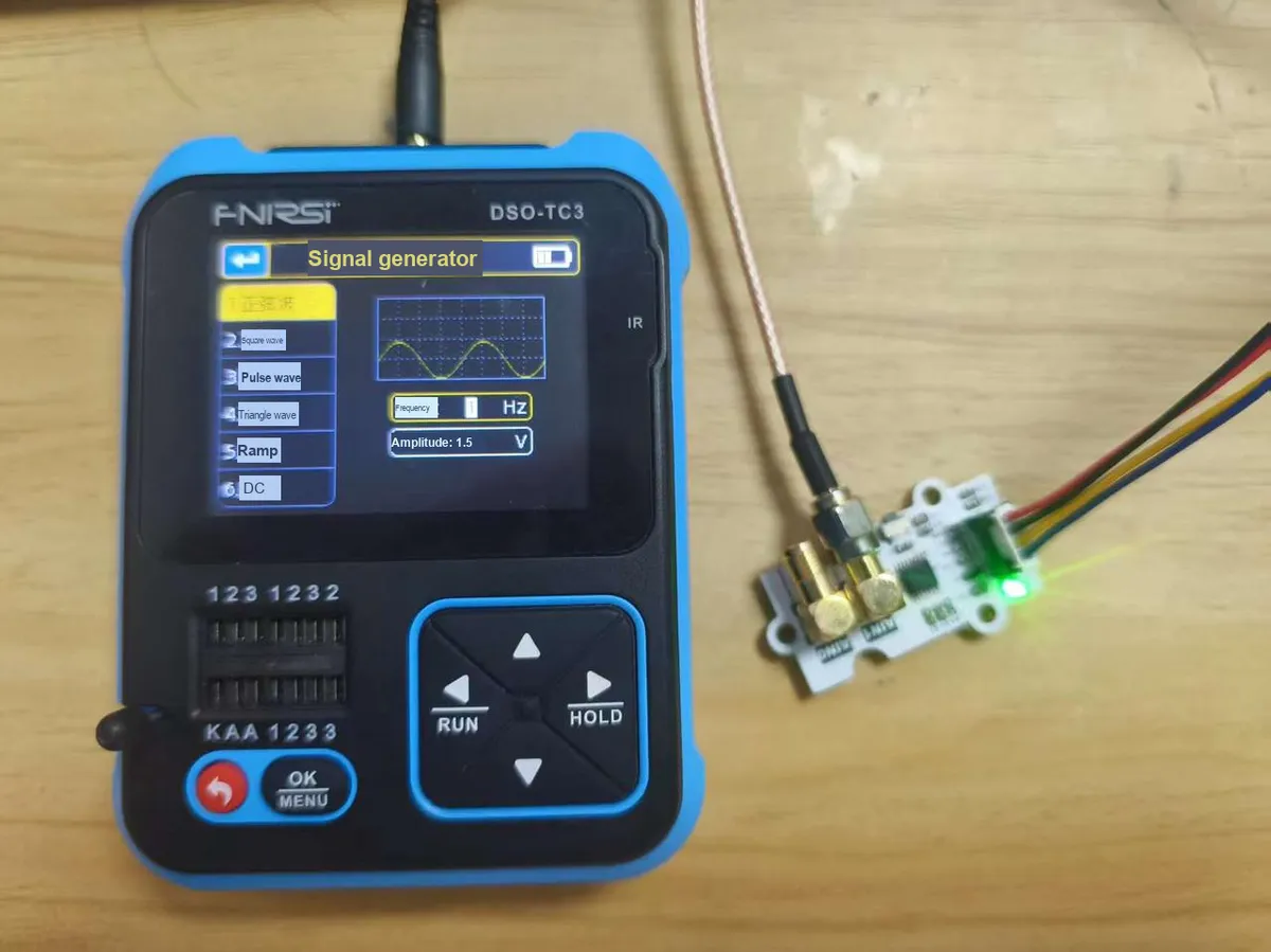
For instructions on using this signal generator, you can refer to the relevant documents below:
17 ADC Analog-to-Digital Conversion - Draft Document Tutorial
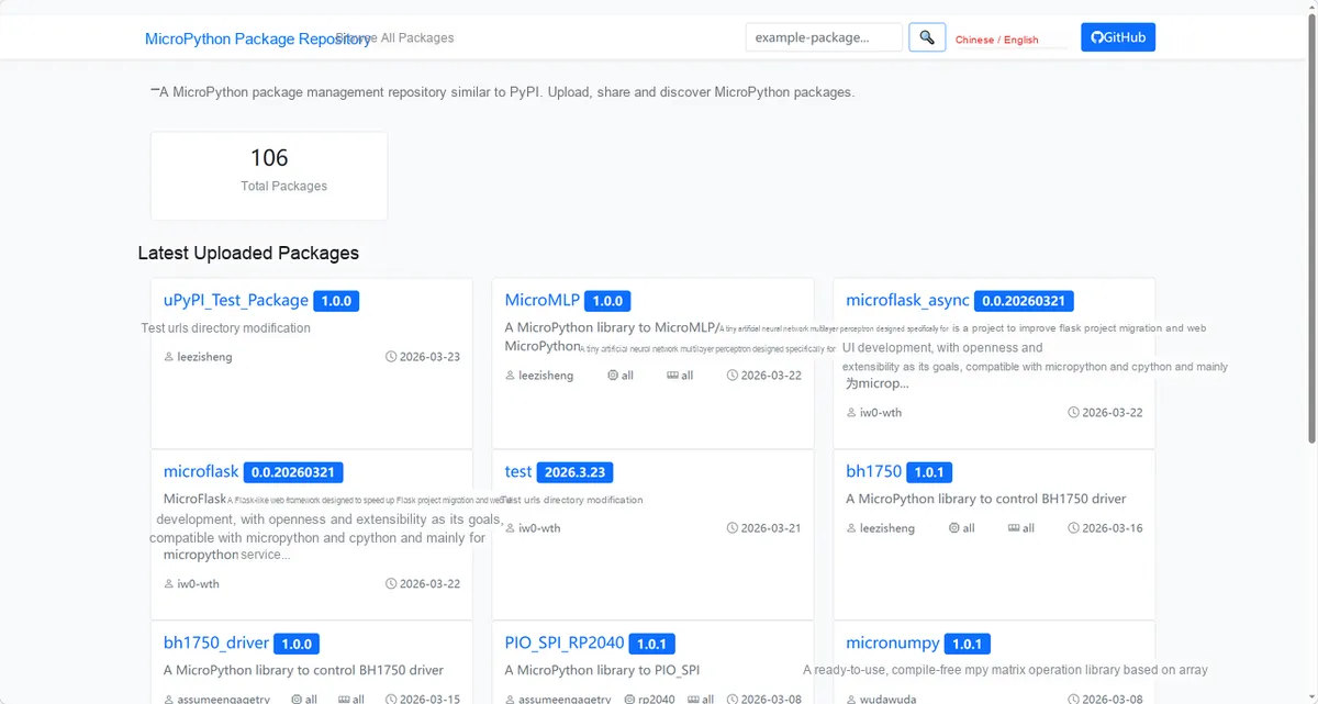
Here, we need to search for the relevant driver packages on uPyPI: https://upypi.net/zh/
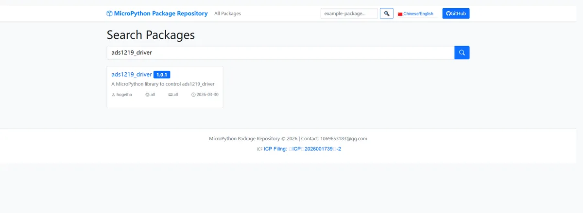
Enter ads1219_driver to search, and the following will be displayed:
Click to copy the local installation command:
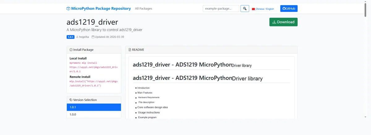
Import the module driver library code via the mip tool. Below are the usage commands for the mpremote tool:
mpremote mip install https://upypi.net/pkgs/ads1219_driver/1.0.0Import the ADS1219-based analog-to-digital conversion module - MicroPython driver code, then copy the following main.py code into our project:
# Python env   : MicroPython v1.23.0
# -*- coding: utf-8 -*-
# @Time    : 2026/3/23 PM 2:23
# @Author  : hogeiha
# @File    : main.py
# @Description : ADS1219 analog-to-digital converter single-shot conversion mode data reading, implementing I2C device scanning, sensor initialization and voltage data acquisition

# ======================================== Import Modules =========================================

# Import the Pin class from the machine module, used to configure hardware pins
from machine import Pin

# Import the I2C class from the machine module, used to control I2C bus communication
from machine import I2C

# Import the ADS1219 class from the ads1219 module, used to operate the ADS1219 analog-to-digital converter
from ads1219 import ADS1219

# Import the utime module, used for delays and other time-related operations
import utime

# ======================================== Global Variables ============================================

# Define the I2C bus SCL pin number (corresponds to GPIO5 of the Raspberry Pi Pico)
I2C_SCL_PIN = 5
# Define the I2C bus SDA pin number (corresponds to GPIO4 of the Raspberry Pi Pico)
I2C_SDA_PIN = 4
# Define the I2C bus communication frequency (standard 100kHz, compliant with the I2C bus specification)
I2C_FREQ = 100000
# Define the list of target I2C addresses of the ADS1219 (the ADDR pin can be configured as 0x40-0x43)
TARGET_SENSOR_ADDR_LIST = [0x40, 0x41, 0x42, 0x43]

# ======================================== Functions ============================================

# ======================================== Custom Classes ============================================

# ======================================== Initialization configuration ===========================================

# Delay 3 seconds to ensure the hardware device completes power-up stabilization
utime.sleep(3)
# Print an initialization message identifying the function purpose
print("FreakStudio: ADS1219 I2C sensor initialization and data acquisition")

# Initialize I2C bus 0, configuring the SCL/SDA pins and communication frequency
i2c_bus = I2C(0, scl=Pin(I2C_SCL_PIN), sda=Pin(I2C_SDA_PIN), freq=I2C_FREQ)

# Scan all devices connected on the I2C bus and return the list of device addresses
devices_list: list[int] = i2c_bus.scan()
# Print I2C scan start message
print("START I2C SCANNER")

# Check the I2C scan result; if no device is found, terminate the program
if len(devices_list) == 0:
    print("No i2c device !")
    raise SystemExit("I2C scan found no devices, program exited")
else:
    # Print the number of I2C devices found
    print("i2c devices found:", len(devices_list))

# Initialize the ADC variable, used to store the ADS1219 sensor instance
adc = None
# Iterate over the scanned I2C device addresses to match the target sensor address
for device in devices_list:
    if device in TARGET_SENSOR_ADDR_LIST:
        # Print the hexadecimal address of the matched I2C device
        print("I2c hexadecimal address:", hex(device))
        try:
            # Initialize the ADS1219 sensor instance
            adc = ADS1219(i2c=i2c_bus ,address=device)
            # Print the sensor initialization success message
            print("ADS1219 sensor initialization successful")
            break
        except Exception as e:
            # Print the sensor initialization failure message and exception details
            print(f"ADS1219 Initialization failed: {e}")
            continue
else:
    # Raise an exception when the target sensor is not found, including the target address and the discovered addresses
    raise Exception(
        f"No ADS1219 found! Target addresses: {[hex(addr) for addr in TARGET_SENSOR_ADDR_LIST]}, "
        f"Found addresses: {[hex(addr) for addr in devices_list]}"
    )

# ========================================  Main Program  ============================================

# Set the ADS1219 sampling channel to the AIN1 channel
adc.set_channel(ADS1219.CHANNEL_AIN1)
# Set the ADS1219 conversion mode to single-shot conversion mode
adc.set_conversion_mode(ADS1219.CM_SINGLE)
# Set the ADS1219 gain to 1x gain
adc.set_gain(ADS1219.GAIN_1X)
# Set the ADS1219 data rate to 20 SPS (conversion accuracy is highest at this rate)
adc.set_data_rate(ADS1219.DR_20_SPS)
# Set the ADS1219 reference voltage to the internal reference voltage
adc.set_vref(ADS1219.VREF_INTERNAL)

# Loop infinitely to read ADS1219 conversion data and print it
while True:
    # Read the data after an ADS1219 single-shot conversion
    result = adc.read_data()
    # Print the raw conversion data and the converted millivolt value
    print("result = {}, mV = {:.2f}".format(result, result * ADS1219.VREF_INTERNAL_MV / ADS1219.POSITIVE_CODE_RANGE))
    # Delay 0.1 seconds to control the data reading frequency
    utime.sleep(0.1)
Burn the code, open the terminal, and the output is as follows:
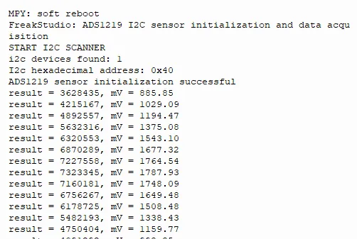
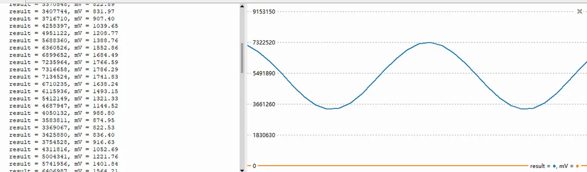
It can be seen that the voltage value can be read cyclically in the single conversion mode normally.
4. Drivers
ads1219_driver-1.0.1.zip 13 KB
5. BOM & Recommended Alternative Parts
None.
VI. Revision History
Document Version | Date of Revision | Modifier | Modify Content |
v1.0 | 2026-03-24 | Ling Gaoxing | Initialize the document |
v1.0.1 | 2026-04-05 | Li Zisheng | No photos for the homepage have been taken, the production files have not been exported yet, and all other items have been sorted out. |
v1.0.2 | 2026-04-21 | Li Zisheng | The production documents have not been exported yet, while all the rest have been sorted out. |
v1.1 | 2026-04-23 | Xin Ruili | Create an open version of the document, based on the internal document version v1.0.2. |
VII. Relevant Materials
7.1 Chip Datasheet
ads1219.pdf 2.0 MB
7.2 PCB Silkscreen Specific Icons