
Contents
- 1. Hardware Explanation
- 1.1 Analog Signals and Digital Signals
- 1.2 Introduction to ADC Peripherals
- 1.3 ADC Peripheral on Raspberry Pi Pico
- 1.4 ADS1115 External ADC Chip
- 2. Software Control Method
- 2.1 Constructor of the machine.ADC class
- 2.2 Other methods of the machine.ADC class
- 3. Application Examples
- 3.1 Periodically collect data from the internal temperature sensor
- 3.2 Simulation Potentiometer Experiment
- 3.3 Joystick Experiment
- 3.4 Reading the External ADC Chip ADS1115 via I2C
- References
- Version History
1. Hardware Explanation
1.1 Analog Signals and Digital Signals
Signals can be classified into digital signals and analog signals according to their continuity and discreteness: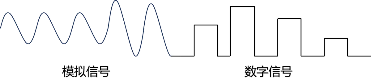
- Analog signal: An analog signal is a type of continuous signal whose amplitude can take an infinite number of values at any point in time. It can vary seamlessly over time and is capable of representing physical phenomena in the real world. For example, sound, light intensity, and temperature are all analog signals.
- Digital signal: A digital signal is a discrete signal that has only a limited number of values, typically 0 and 1. Represented in binary form, a digital signal makes it particularly suitable for use in computers and digital electronic systems. All data we process in computers is in the form of digital signals. For example, when music is stored on a CD or transmitted via a Streaming Media service, it is converted into digital signals composed of a series of 0s and 1s; image files (such as JPEG and PNG) also exist as digital signals during storage and transmission, with each pixel represented as a numerical value.
The difference between the two is that an analog signal is continuous and can take any value in terms of time and amplitude, whereas a digital signal is discrete and can only take a limited number of values:
- Analog signals are more sensitive to noise and susceptible to interference, whereas digital signals have better resistance to noise, as they only need to distinguish between 0 and 1.
- Digital signals are easier to store and transmit, and can be accurately copied via digital circuits, whereas analog signals may suffer from distortion during copying and transmission.
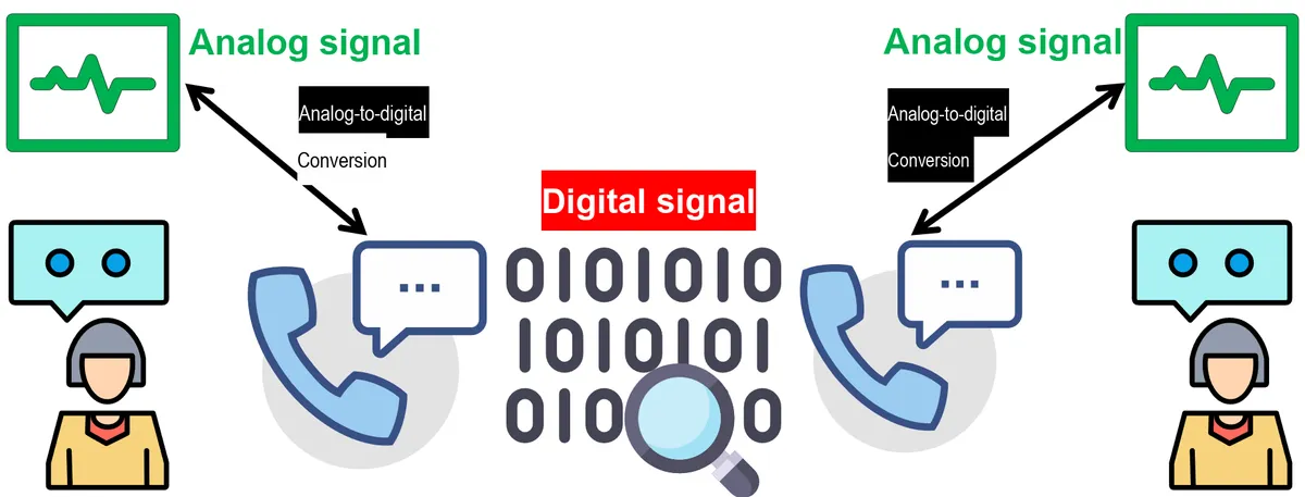
Analog data from external sensors often needs to be converted into digital signals via an ADC (Analog-to-Digital Converter) before being processed and transmitted in a computer. For instance, imagine you are on a call with a friend: your voice is continuous and ever-changing, which is a type of analog signal. To be transmitted over the phone, however, it has to be converted into a digital signal that computers can recognize and process — that is, binary numbers made up of 0s and 1s. Your voice is sampled by the phone, then each tiny segment is converted into digital bits of 0s and 1s and transmitted to the recipient's phone.The other party's phone then converts these digital bits back into an analog signal, so your friend can hear your voice.
1.2 Introduction to ADC Peripherals
An Analog-to-Digital Converter (ADC) is an electronic device that converts analog signals into digital signals. It is widely used in various electronic equipment, such as sensor interfaces, audio processing, measuring instruments, etc. In modern electronic design, ADC plays a crucial role.

ADCs are present in almost all electronic devices that require converting analog signals to digital signals. Common applications include:
- Audio Equipment: In microphones, audio recording devices and digital audio players, it converts sound signals into digital signals for processing and storage.
- Sensor Interface: Converts analog signals output by sensors such as temperature, pressure, and light intensity into digital signals for data processing and control
- Data Acquisition System: In experiments and industrial control, it uses ADCs to collect analog signals for monitoring and analysis
- Communication system: In radio communication, analog signals are digitized for modulation, coding and transmission
- Image Processing: In cameras and image sensors, an ADC is used to convert optical signals into digital signals for subsequent image processing and storage.
1.2.1 Basic Structure and Working Principle of ADC
The basic structure of an ADC consists of the following components: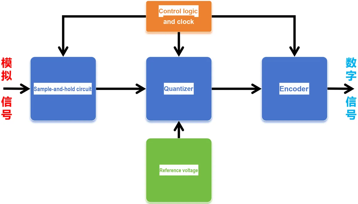
- Sample and Hold Circuit: The function of the sample and hold circuit is to sample a continuous analog input signal at a specific time point and hold the voltage value of that instant until the next sampling moment. This is because the ADC requires a stable input signal during the conversion process to obtain an accurate digital output.
- Quantizer: A quantizer divides the voltage value held by the sample-and-hold circuit into a number of discrete levels, which correspond to possible digital outputs. The quantization process introduces quantization error, meaning that the analog signal cannot be accurately mapped to a certain digital value, thus resulting in some distortion.
- Encoder: The encoder converts the quantized discrete levels into binary codes, i. e., digital signals. This process involves mapping the amplitude of the input signal to a set of fixed binary values.
- Reference Voltage: The reference voltage defines the range of quantization levels, specifying the maximum and minimum input voltages that an ADC can handle; the input signal is quantized into an appropriate binary number relative to the reference voltage.
- Control Logic and Clock: The control logic is used to manage the operations of the ADC, including controlling the sampling time and initiating the conversion process. The clock signal serves to synchronize various processes, ensuring that sampling, holding, quantization and encoding are carried out in sequence.
The basic function of an ADC is to convert continuously varying analog signals (such as voltage) into a series of discrete digital values, and its working process generally includes the following steps:
- Sampling: The process of discretizing an analog signal in the time domain, that is, sampling the signal at regular time intervals; the sampling frequency determines the maximum signal frequency that an ADC can capture, and according to the Nyquist theorem, the sampling frequency shall be at least twice the signal bandwidth
- Quantization: Converting the sampled analog signal values into discrete levels, the number of quantization levels is determined by the resolution of the ADC; for example, an 8-bit ADC has 256 quantization levels.
- Encoding: Convert the quantized signal values into binary codes for the processing and storage of digital systems, and the number of encoding bits is equal to the resolution of the ADC
Here, we take the AD conversion process of a sine wave as an example to explain the workflow in ADC conversion.
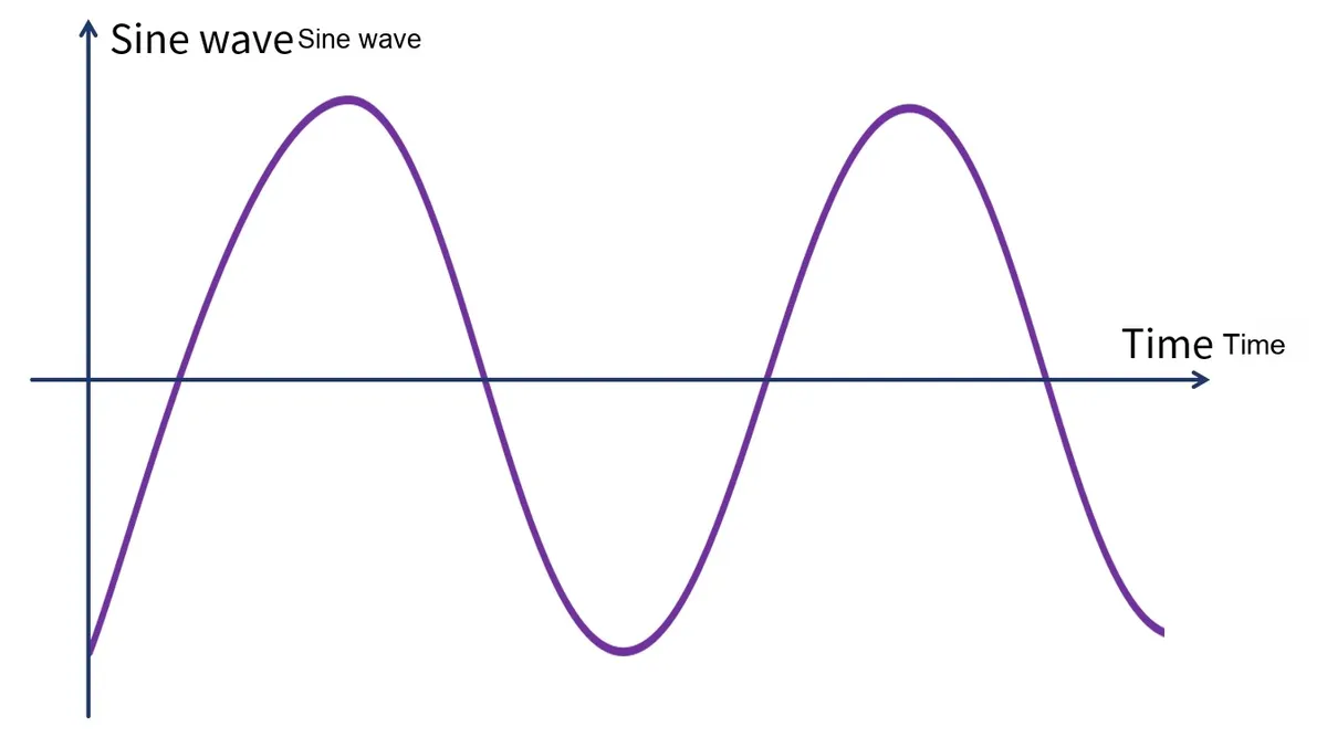
It is continuous in both time and amplitude, and this is the signal we need to process. This analog signal is fed into a sample-and-hold circuit composed of a sampler switch. The sampler switch is typically a simple switch that closes and opens at the sampling frequency, as shown in the figure below. When the switch is closed, the signal amplitude at this time point can be obtained at the output of the switch, and its value will be held.
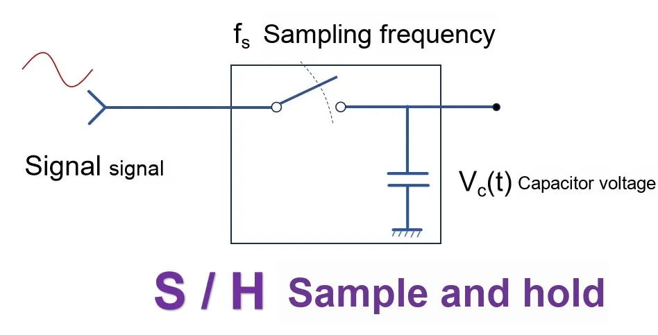
Its holding function is realized by a capacitor connected to the output terminal of the sampling switch. When the switch is closed, the capacitor is charged to the voltage value of the analog signal at that time point. When the sampling process is completed, the switch is turned off, and the capacitor will maintain the voltage value of the analog signal during sampling until the next sampling instant.
The graph of the capacitor voltage (i. e., the sampling signal) as a function of time is shown below:
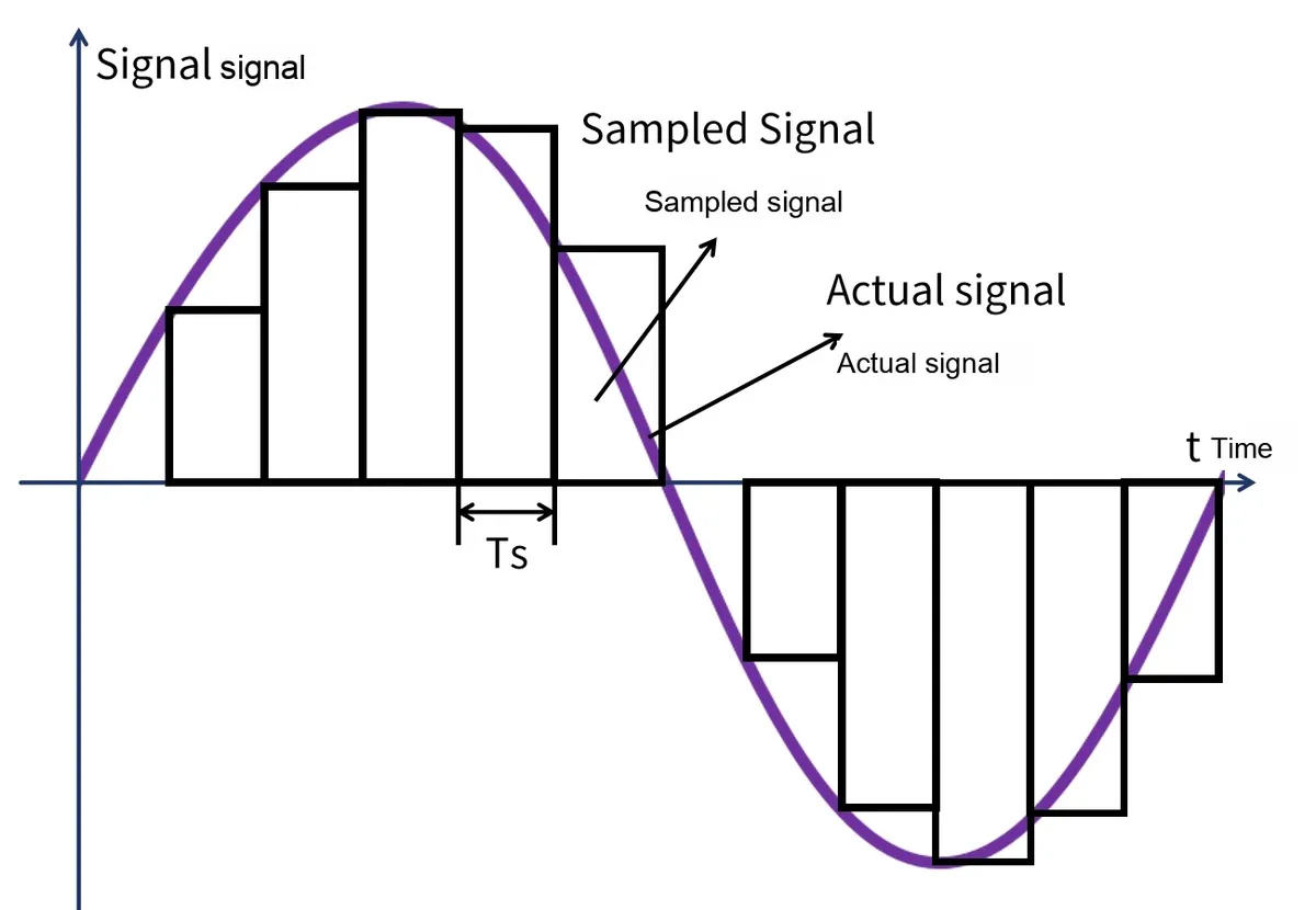
It is evident that sampling cannot reflect the amplitude of a signal with perfect accuracy, and there is a noticeable error between the sampled voltage and the sinusoidal signal. This error is unavoidable in the sampling process, but it can be reduced by increasing the sampling frequency. However, an excessively high sampling frequency will lead to increased requirements for processing and storage.
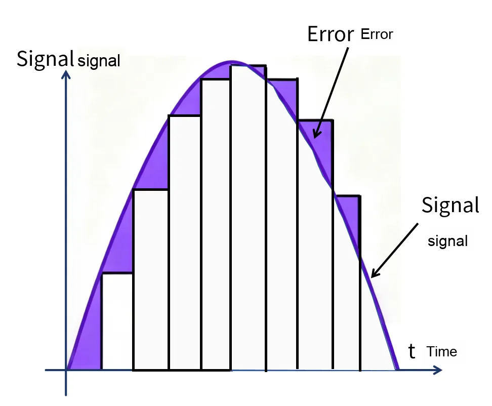
The voltage value of the capacitor is then sent to the quantizer. As we can see above, the output voltage of the capacitor appears as time-continuous rectangular bars, with the amplitude remaining constant within each sampling interval. The quantizer divides the voltage value held by the sample-and-hold circuit into several discrete levels; simply put, it maps the voltage value represented by the corresponding rectangular bar within each sampling interval into a binary value composed of 0s and 1s.
Suppose we have a 3-bit ADC with an input voltage range from 0V to 1V, and the full voltage range will be mapped to a total of 8 three-bit binary numbers from 000 to 111. Then the resolution of this ADC is:.
With a resolution of 0.125V, the output digital value will be 000 for all input signal amplitudes ranging from 0V to 0.125V; when the voltage falls between 0.125V and 0.250V, the mapped value is 001; when the signal amplitude is between 0.250V and 0.375V, the output digital value is 010. The transfer curve of the aforementioned conversion is shown in the following figure:
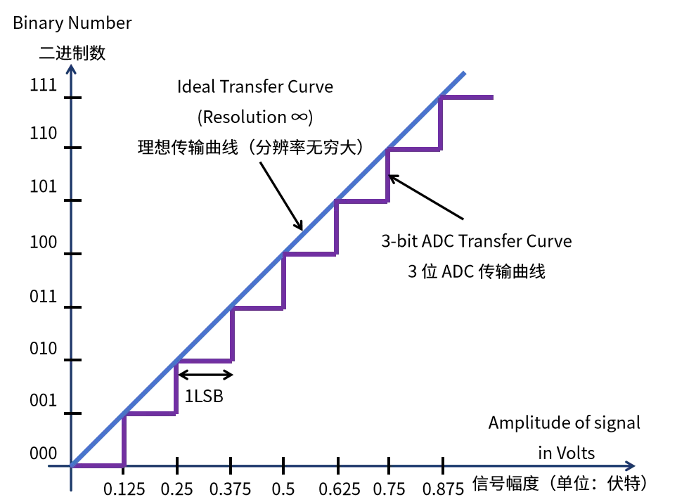
In this process, we will encounter the problem of quantization error. For example, for the amplitude of an analog signal between 0V and 0.125V, the output is always the same 000 code. This leads to information loss, because any value between 0V and 0.125V is processed as the same digital value. Quantization error can be reduced by decreasing the resolution voltage, that is, adding more digital output bits for the same input voltage.
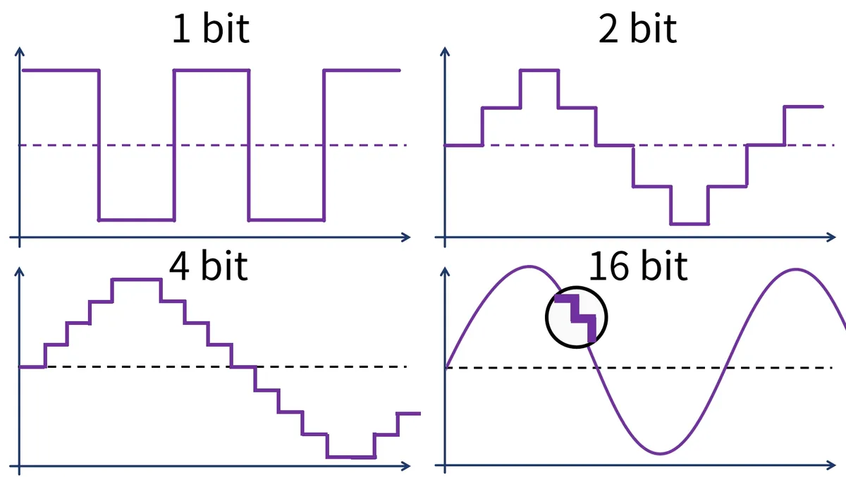
Finally, the quantized discrete levels are converted into binary codes, namely digital signals, by an encoder.
1.2.2 Performance Indicators of ADC
When selecting and using an ADC, the following key indicators require attention:
- Resolution (Resolution): The number of binary bits output by the ADC determines the accuracy of the conversion result. The higher the resolution, the more quantization levels the signal has, and the finer the output result. Common resolutions include 8-bit, 10-bit, 12-bit, 16-bit, etc.
- Sampling Rate: The number of times an ADC samples an analog signal per unit time. The sampling rate determines the maximum signal frequency that an ADC can process. The commonly used unit is Samples Per Second (SPS).
- Signal-to-Noise Ratio (SNR): The ratio of the input signal to the noise component in the ADC output. A higher SNR indicates that the ADC has stronger anti-noise capability and produces a purer output signal.
- Effective Number of Bits (ENOB): It represents the actual resolution of an ADC, which takes into account the impacts of signal-to-noise ratio and nonlinear errors. A higher ENOOB indicates that the performance of the ADC is closer to the ideal state.
- Total Harmonic Distortion (THD): A metric that quantifies the harmonic components in an ADC's output signal caused by nonlinear distortion; a lower THD value indicates better linearity of the ADC.
- Differential Non-Linearity (DNL): refers to the degree of deviation between the voltage difference between adjacent quantization levels and the ideal difference. DNL affects the accuracy and resolution of an ADC
- Integral Non-Linearity (INL): refers to the maximum deviation between the actual conversion curve of an ADC and the ideal straight line, and INL also affects the accuracy of the ADC
- Input Range: The voltage range of the analog input signal that an ADC can correctly convert; signals beyond this range will result in errors.
- Power Consumption: The electrical energy consumed by an ADC during operation, which is closely related to the application scenarios of the ADC, especially in battery-powered portable devices.
1.2.3 Types of ADCs
From the perspective of whether it is integrated into the MCU, ADCs can be divided into built-in on-chip ADCs and external ADC chips: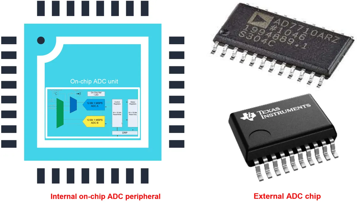
- Built-in on-chip ADC: A built-in ADC is an integral part of a microcontroller or SoC (System-on-Chip), which requires no external interface circuitry, occupies a small area on the PCB, and simplifies the design. It features the advantages of low power consumption, fast response speed and low cost. However, limited by the chip area, power consumption and noise, the resolution and accuracy of an on-chip ADC are generally not as high as those of an external ADC, and the common resolution of on-chip ADCs ranges from 8 to 12 bits.
- External ADC chip: External ADC chips usually offer higher resolution (16-bit, 24-bit or even higher) and better accuracy, which can meet the requirements of high-precision measurement. We can select appropriate ADC chips according to application needs, such as high-speed sampling ADCs, high-precision low-speed ADCs, etc. They provide better power supply and signal noise isolation, but require external circuits for connection, which increases the complexity of PCB design and the occupied area. Meanwhile, the driving capability and signal integrity of the interface need to be considered, and the power consumption is relatively high.
Simply put, the built-in on-chip ADC is suitable for application scenarios such as general sensor signal acquisition, simple audio signal processing, and low-cost portable devices, while external ADC chips are commonly used in scenarios with high requirements for resolution and accuracy, such as high-precision measurement instruments, high-speed Data Acquisition systems, audio and video processing, and professional medical equipment.
From the perspective of working principles, ADCs can be classified into the following types:
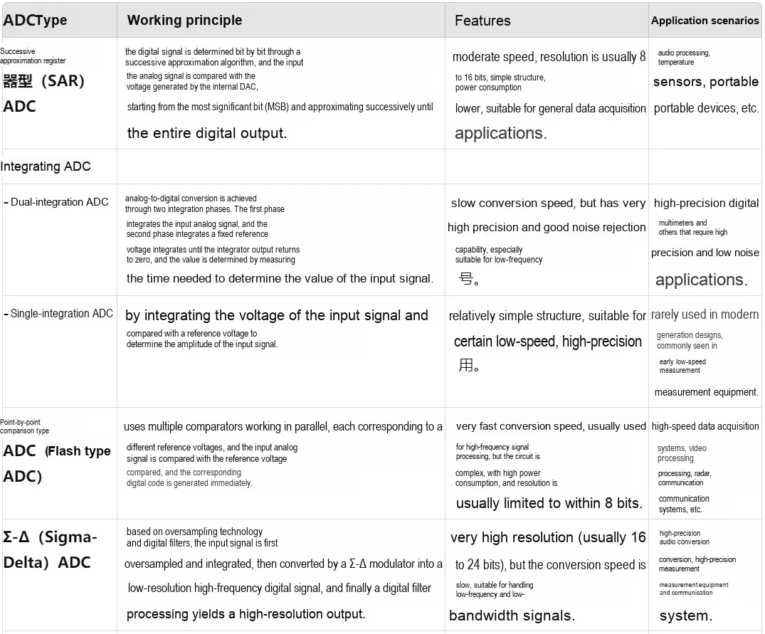
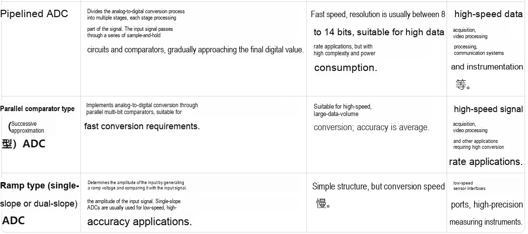
Each type of ADC has its unique working principle and applicable scenarios, and selecting the appropriate ADC type according to application requirements is the key to realizing efficient Data Acquisition and processing.
1.3 ADC Peripheral on Raspberry Pi Pico
1.3.1 Introduction to ADC Peripherals
The RP2040 incorporates a built-in Successive Approximation Register (SAR) ADC, which operates with an independent 48MHz clock and supports a maximum sampling rate of up to 500ksps (500,000 samples per second), making it suitable for medium-speed signal acquisition. This ADC has a resolution of 12 bits, meaning it can convert analog signals into 4096 (2^12) distinct digital values; its Effective Number of Bits (ENOB) is 8.7, which indicates the actual achievable precision.
Effective Number of Bits (ENOB)
ENOB (Effective Number of Bits, effective number of bits) is an indicator that describes the actual performance of an analog-to-digital converter (ADC). It reflects the level of accuracy that an ADC can achieve when processing real-world signals. Although an ADC may be specified to have a resolution of 12 bits, 16 bits, etc. , the actual effective number of bits it can reflect is usually lower than the nominal value due to various noises, distortions and non-ideal effects. ENOB is the number of bits that can truly reflect the accuracy of an ADC after taking these non-ideal factors into account.
The connection between the ADC peripheral built into the RP2040 and the GPIO pins is as follows:
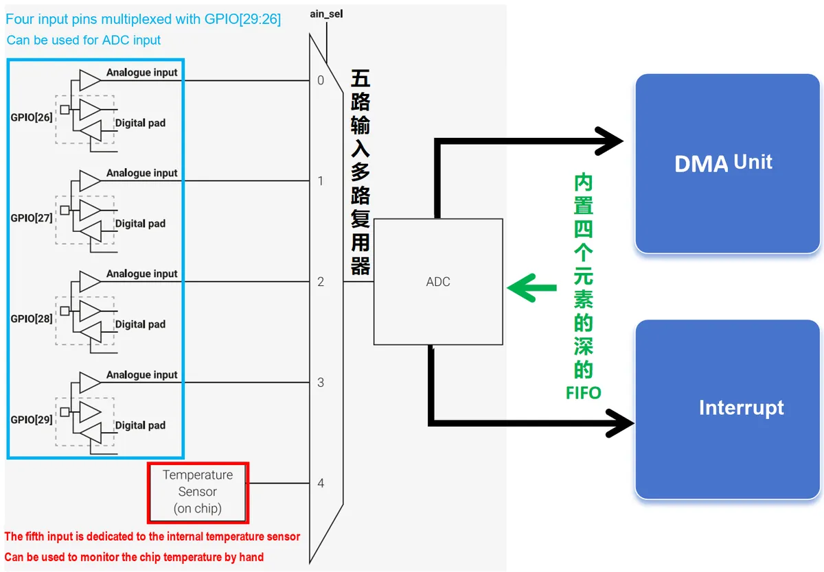
Here, a digital controller is specifically responsible for managing the operation of the ADC and provides additional functions:
- Single sampling mode or free-running sampling mode: The ADC can be configured to perform only one sampling (One-shot mode) or to perform continuous sampling (free-running capture mode)
- Sampling FIFO with DMA Interface: The data sampled by the ADC will be stored in a FIFO buffer, and can be transferred to the system memory via the DMA (Direct Memory Access) interface to reduce the load on the CPU
- Beat Timer: This timer features a resolution of 16-bit integer plus 8-bit fraction, which is used to set the sampling rate in free-running mode, and the beat timer can precisely control the sampling time interval.
- Polling to sample multiple channels: In free-running mode, the ADC can sample multiple input channels in turn instead of being limited to a single channel, which is very useful when multiple signals need to be acquired simultaneously
- Optional right shift to 8 bits: In free-running mode, the sampling result can be selectively right-shifted to 8 bits, so that the sampled data can be transferred to the buffer in the system memory via DMA in the form of bytes (8 bits), which is more convenient for reducing memory usage and processing byte data
When using the ADC peripheral, it is necessary to ensure that the digital function of the pin is disabled. This can be achieved by setting the IE bit (input enable) in the Pad Control register of the pin to a low level (IE = 0) and the OD bit (open-drain drive) to a high level (OD = 1).
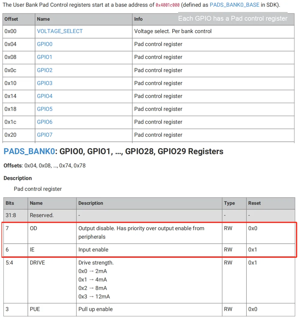
In addition, the maximum input voltage of the ADC is determined by the supply voltage of the digital IO (IOVDD), rather than the supply voltage of the ADC (ADC_AVDD). For example, if the IOVDD supply voltage is 1.8V, then even if the ADC_AVDD supply voltage is 3.3V, the ADC input voltage should not exceed 1.8V. Otherwise, a voltage exceeding IOVDD will cause a leakage current through the ESD protection diode, which may damage the chip.
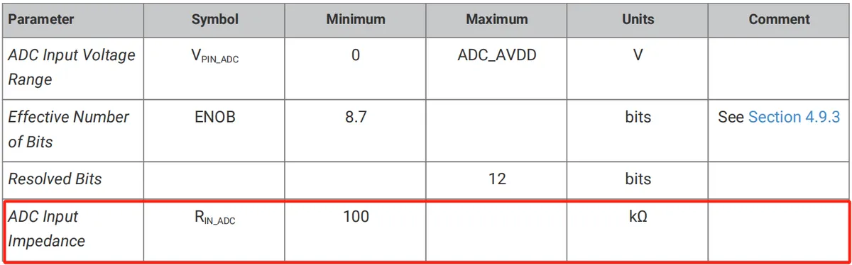
The input impedance of the ADC pins on the Raspberry Pi Pico is approximately 100KΩ, which is suitable for most applications. If the impedance of the signal source is higher than the ADC input impedance, it may cause signal attenuation and reduce measurement accuracy.
As we mentioned earlier, the RP2040 has a built-in Successive Approximation Register (SAR) ADC, whose structural block diagram is shown below:
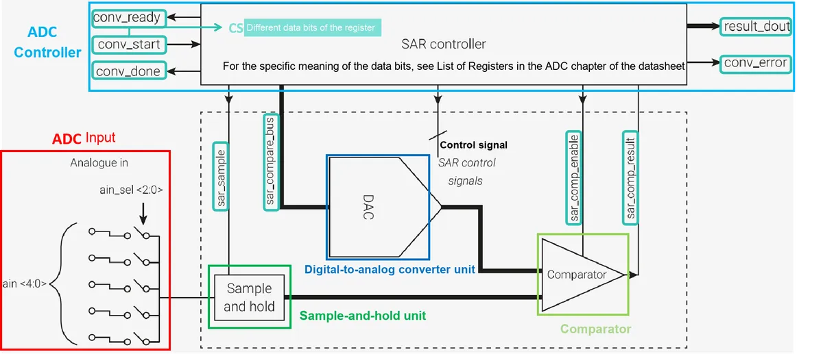
The operating process of a SAR ADC can be summarized as follows:
- Successive Approximation: A SAR ADC performs analog-to-digital conversion via a successive approximation algorithm. First, it starts from the most significant bit (MSB), sets this bit to 1, and then converts this digital signal into an analog voltage through an internal DAC.
- Comparator Comparison: Then, the generated analog voltage is compared with the input analog signal; if the voltage generated by the DAC is higher than the input analog signal, the SAR will clear this bit; if it is lower, the bit will remain 1
- Continue bit-by-bit approximation: This process proceeds sequentially, determining the value of each bit one by one until all bits are finalized.
- Final Output: After the successive approximation of all bits is completed, the final digital value represents the digitized result of the input analog signal.
The DAC unit continuously generates different voltage values during this process and compares them with the input signal to gradually determine the digital value of the input signal. Therefore, the accuracy and linearity of the DAC are critical to the overall performance of the SAR ADC. In the ADC of the RP2040, this DAC unit is built-in, and no external DAC module is required to complete the analog-to-digital conversion process.
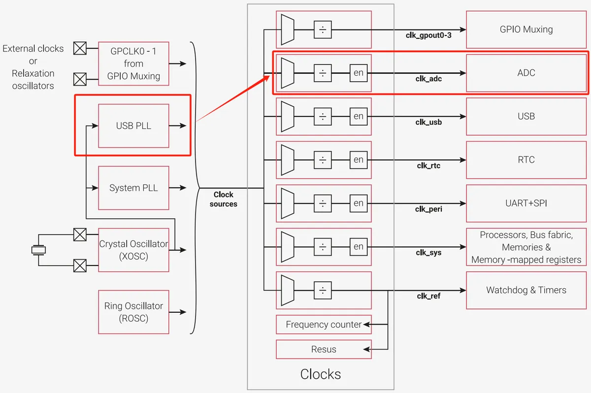
SAR ADC (Successive Approximation Register Analog-to-Digital Converter) consists of a combination of a digital controller and analog circuits. This ADC requires a 48MHz clock (clk_adc), which can be sourced from the USB PLL (Phase-Locked Loop). One sampling operation takes 96 clock cycles (96 × 1/48MHz) = 2 microseconds when the sampling rate is 500ksps. The clock must be properly configured before enabling the ADC.
Once the ADC module is provided with a clock and its reset is released, setting the EN bit of the CS control register to 1 will trigger a brief internal power-up sequence for the analog hardware of the ADC; after several clock cycles, the READY bit of the CS control register will go high, indicating that the ADC is ready to start the first conversion.
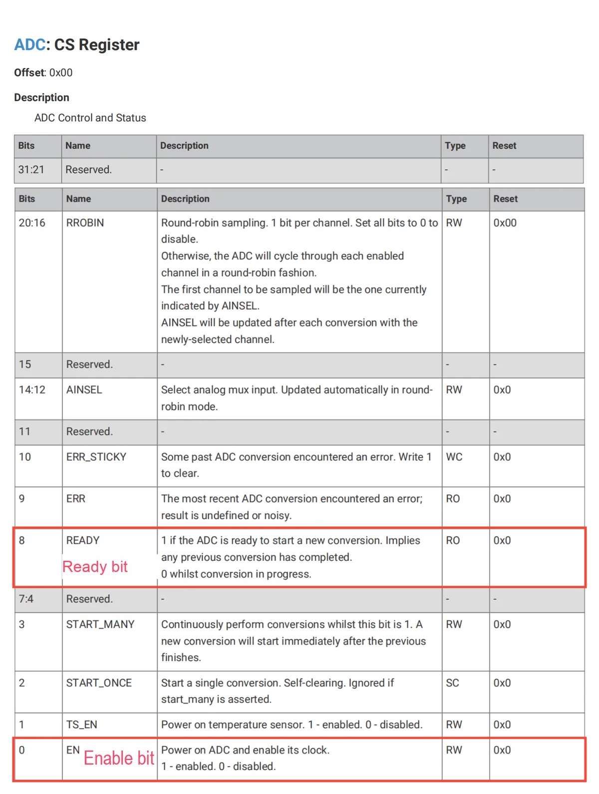
The ADC can be disabled at any time by clearing the EN bit in the CS control register to save power. It should be noted that the ADC input is capacitive, with a built-in 1pF capacitor at the input terminal, and its effective impedance exceeds 100kΩ even at a sampling rate of 500ksps, so buffering is generally not required for DC measurements.
1.3.2 ADC Operating Mode
The ADC of the RP2040 supports two selectable operating modes:
- Single Sampling Mode: This mode is applicable to scenarios where a one-time analog-to-digital conversion is required at a specific moment. After a conversion is initiated, the ADC will complete the sampling and return the result within 96 clock cycles.
- Free-running sampling mode: This mode is suitable for scenarios requiring continuous sampling, such as real-time Data Acquisition. The ADC will automatically start the next conversion immediately after completing one conversion, unless a delay is deliberately set.
1.3.2.1 Single Sampling Mode
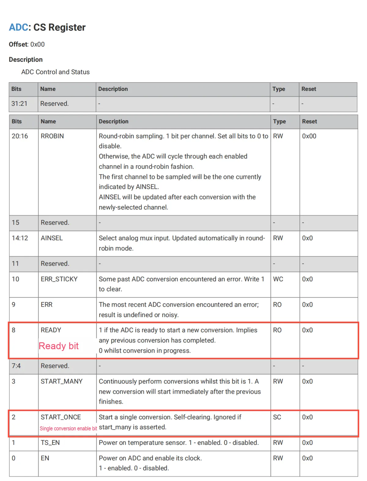
In single sampling mode, by writing 1 to the CS.START_ONCE data bit, a new analog-to-digital conversion process can be started immediately. When the conversion starts, the CS.READY data bit will go low, indicating that a conversion is currently in progress. After 96 clk_adc clock cycles, the CS.READY data bit will go high again, indicating that the conversion has been completed.
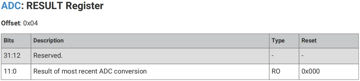
After the conversion is completed, the 12-bit conversion result will be stored in the RESULT register.
Before starting the conversion, you can select the ADC input channel to be sampled by writing to the CS.AINSEL data bits. When the value of AINSEL ranges from 0 to 3, the ADC input channels corresponding to GPIO 26 to 29 are selected; when the value of AINSEL is 4, the internal temperature sensor is selected.
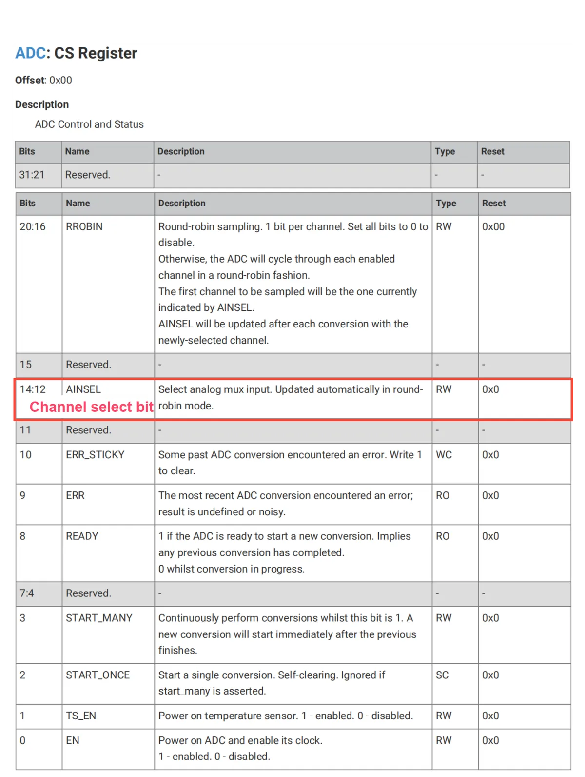
It should be noted that when switching AINSEL values, there is no need to wait for the steady-state time, which means you can freely switch the input channels before the conversion starts without negatively affecting the conversion results.
1.3.2.2 Free-running sampling mode
In free-running sampling mode, by setting the CS.START_MANY bit, the ADC will automatically initiate new conversions at fixed intervals. The latest conversion result is always stored in the RESULT register. However, if sampling data needs to be transferred via interrupt (IRQ) or DMA, the ADC's FIFO must be enabled.
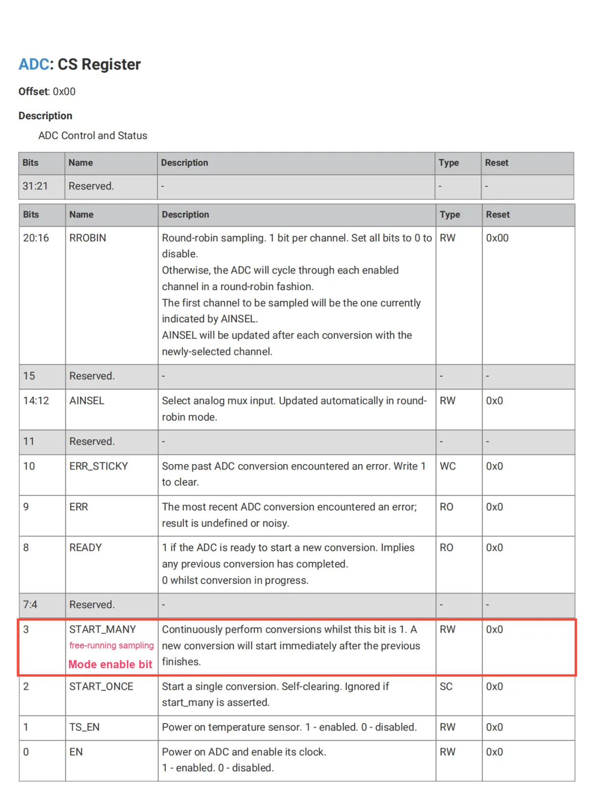
By adjusting the DIV.INT and DIV.FRAC data bits of the DIV frequency division register, the sampling rate can be controlled:
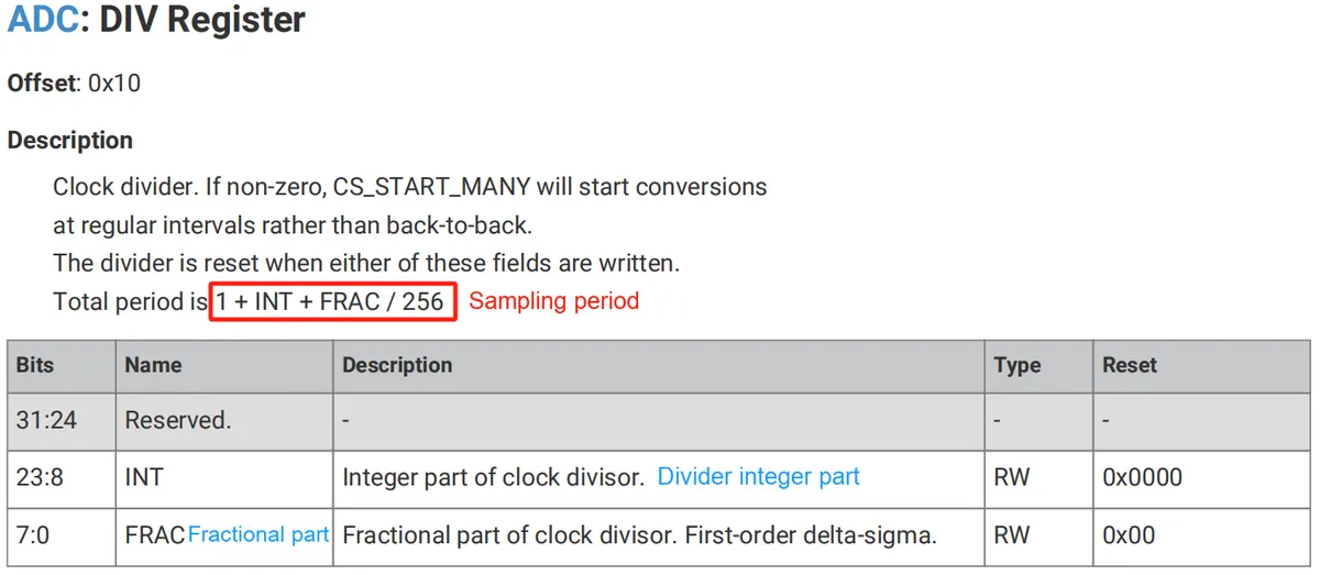
By default (DIV = 0), a new conversion starts immediately after the previous one completes, resulting in a new sampled data every 96 clock cycles. Assuming a clock frequency of 48MHz, this gives the ADC a sampling rate of 500k samples per second (ksps).
If DIV.INT is set to a positive value n, the ADC will be triggered once every n + 1 clock cycles. However, if a conversion is currently in progress, the ADC will ignore the trigger signal, so n should generally be greater than or equal to 96. For example, when DIV.INT is set to 47999, the ADC will operate at a rate of 1k samples per second when using a 48MHz clock.
The timer supports fractional-rate frequency division. When the DIV.FRAC data bits are set to a non-zero value, the ADC initiates a new conversion on average once every 1 + INT + FRAC/256 clock cycles, which is achieved by varying the sampling interval between INT + 1 and INT + 2.
1.3.3 Multi-input Sampling
By setting the RROBIN data bit in the CS register, the multi-input sampling mode can be enabled, which allows the ADC to automatically switch and sample different input channels, thus realizing the function of automatically and alternately collecting data from multiple input channels in the free-running mode without manual intervention:
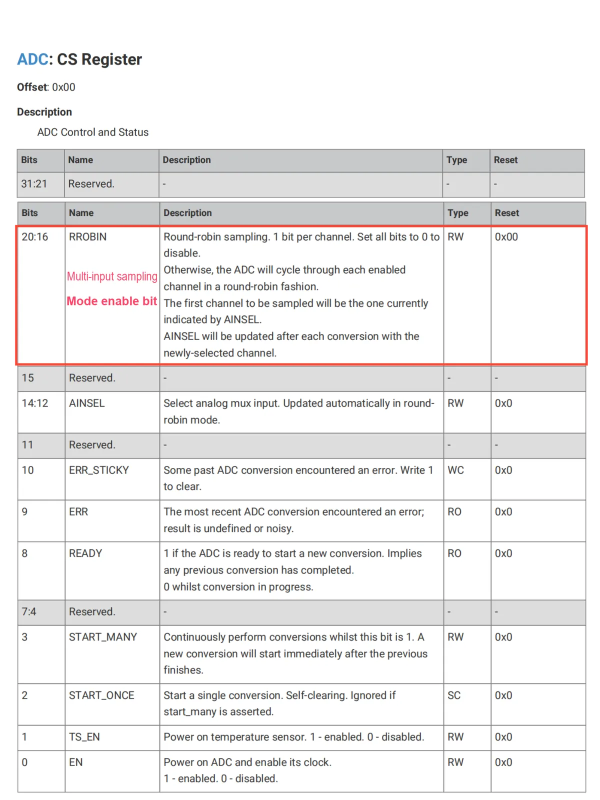
In the CS.RROBIN data bits, setting a certain bit to 1 will cause the corresponding input channel to be automatically sampled by the ADC. When multiple bits are set to 1, the ADC will sample these channels in turn according to their order; if all bits in CS.RROBIN are set to 0, the cyclic sampling function will be disabled, that is, the ADC will only continuously sample the channel specified by the current CS.AINSEL.
Even if AINSEL 's initial value is not among the channels specified by RROBIN, the ADC will still start operating from the current channel and sample the channels configured in RROBIN one by one. For example, if AINSEL ' s initial value is 0 and RROBIN is set to 0x06 (i. e., only bits 1 and 2 are set), the ADC will perform channel sampling in the following order:
- Channel 0
- Channel 1
- Channel 2
- Channel 1
- Channel 2
- Channel 1.. .
and will repeatedly sample in this order until disabled CS.RROBIN data bits.
1.3.4 Sampling Receive FIFO
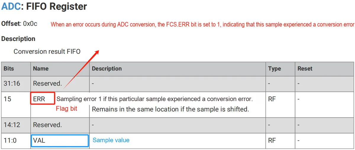
In the ADC module of the RP2040, the sampling result can be read directly from the RESULT register, or stored in a local receive FIFO buffer which we read out via the FIFO register.
FIFO operation is controlled by FCS FIFO control register:
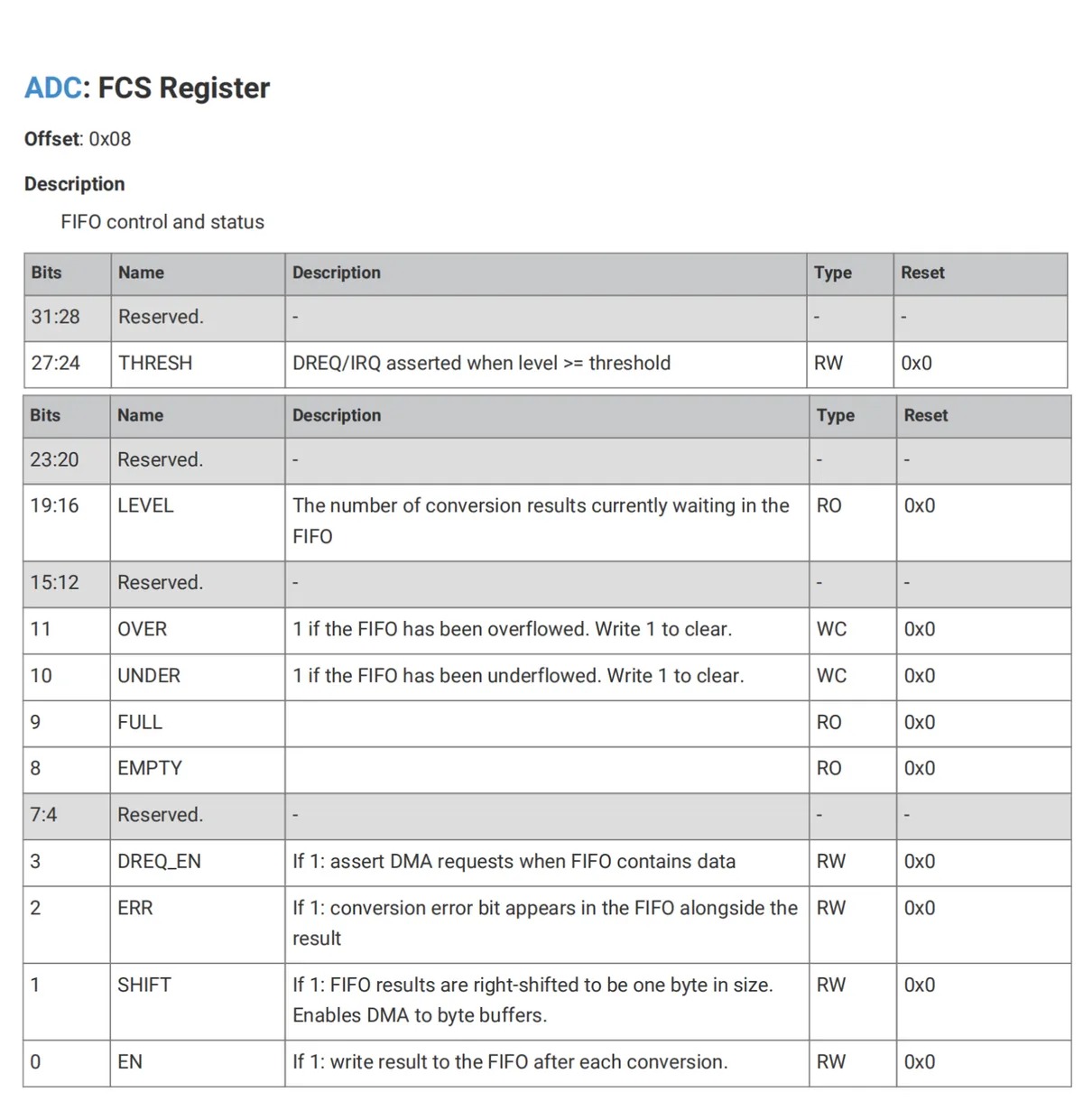
The meanings of the respective flag bits are as follows:
data bit | Name | Meaning |
THRESH | of DREQ/IRQ trigger threshold | When the amount of data in the FIFO is greater than or equal to the set threshold, the DREQ or IRQ signal will be triggered. |
LEVEL | to be processed Number of conversion results | Indicates the number of conversion results currently stored in the FIFO, and this value represents how many ADC conversion results are waiting to be read in the FIFO |
OVER | FIFO overflow flag bit | When the FIFO is already full upon the completion of ADC conversion, making it impossible to write the new conversion result into the FIFO, the OVER flag bit will be set to 1, indicating that the FIFO has overflowed and some conversion results have been lost. Write 1 to clear this flag. |
UNDER | FIFO underflow flag | When software or a DMA attempts to read data from an empty FIFO, the UNDER flag will be set to 1, indicating that a FIFO underflow has occurred and invalid data has been read. Write 1 to clear this flag. |
FULL | FIFO full flag | This bit is set to 1 when the FIFO is full. |
EMPTY | FIFO empty flag bit | This bit is 1 when the FIFO is empty. |
DREQ_EN | DMA request enable bit | When set to 1, a DMA request will be triggered if the amount of data in the FIFO is greater than the value set in THRESH. |
ERR | Conversion Error Enable Bit | When set to 1, the conversion error bit will appear in the FIFO together with the result. |
SHIFT | Shift Right Enable Bit | When set to 1, the results in the FIFO will be shifted right by 4 bits to become 8-bit bytes. When enabled, data can be transferred to the byte buffer via DMA. |
EN | FIFO write enable bit | When set to 1, the result will be written to the FIFO after each conversion. |
1.3.4.1 FIFO Enable and Read
When FCS.EN data bit is set to 1, the result of each ADC conversion will be written to the FIFO. At this point, we can:
- The software polls the status bits of the FCS register and reads each sampled data when it becomes available.
- Use interrupt or DMA to read the sampling data from the FIFO after receiving the IRQ interrupt signal from the ADC or the DREQ DMA request signal
1.3.4.2 FIFO Overflow
If a new conversion result arrives when the FIFO is full, the FCS.OVER error flag will be set, but the existing data in the FIFO will not be overwritten; in this case, subsequent conversion results will be lost.
1.3.4.3 FIFO Data Write Format
The FCS register has two bits used to control the format of data written to the FIFO:
FCS.SHIFTbit: When set to 1, the data in the FIFO will be shifted right by 4 bits (bits 7:0 of the FIFO correspond to bits 11:4 of the conversion result). This facilitates 8-bit DMA transfer to a byte buffer to achieve a deeper capture buffer, at the cost of some precision.FCS.ERRbit: When set to 1, the ERR flag bit of each value in the FIFO will be set, indicating that a conversion error has occurred. In this case, we should try to use the data obtained from the next sampling or increase the conversion time.
It should be noted that although the FIFO data has been shifted, the FIFO.ERR flag bit will remain in its original position and still indicate whether a conversion error has occurred for this sample; in other words, even if FCS.SHIFT is enabled to reduce the FIFO data width, the FIFO.ERR flag bit will still accurately indicate whether the sample has experienced a conversion error and will not change due to data shifting.
These errors indicate that the comparison of one or more bits failed to complete within the specified time. Typically, this is caused by comparator metastability, meaning that when the input signal is close to the comparator threshold, the transition takes longer.
1.3.4.4 Use of FIFO in conjunction with DMA
The DMA controller of the RP2040 can acquire ADC samples by reading the ADC sample FIFO register, and this process is controlled by the ADC_DREQ system data request signal. When using DMA to transfer ADC data, the following points should be noted:
- Enable FIFO (FCS.EN): The FIFO must be enabled to allow ADC conversion results to be written to the FIFO. By default, the FIFO is disabled to prevent accidental FIFO filling during single-shot conversion operations.
- Enable ADC DMA Request (FCS.DREQ_EN): The ADC DMA request signal DREQ must be enabled so that the DMA can read data from the FIFO according to the ADC's request signal.
- Select the DREQ_ADC data request signal for the DMA channel: The DMA channel in use must select the DREQ_ADC data request signal to ensure that the DMA can operate in synchronization with the ADC's data request signal.
- Set the DREQ assertion threshold (FCS.THRESH): The DREQ assertion threshold should be set to 1 so that the DMA starts transmission as soon as there is one sample in the FIFO. Note that this is also the threshold for IRQ assertion, so in non-DMA usage scenarios, a higher value may be required to reduce the interrupt frequency.
- Configuration for 8-bit DMA transfer: If the DMA transfer size is set to 8 bits (i. e., data is transferred to a byte array in memory), FCS.SHIFT must be enabled to pre-right-shift the FIFO samples into one byte of data.
- Multi-channel sampling configuration: If sampling of multiple input channels is required, a 5-bit mask for the corresponding channels (including 4 external input channels and the temperature sensor) can be set in
CS.RROBIN; in addition, the first sampling channel must be selected viaCS.AINSEL. - Configure the ADC sampling rate: Before starting the ADC, the ADC sampling rate should be configured properly in advance.
After configuring the ADC, start the DMA channel first, then initiate ADC conversion (by setting the CS.START_MANY bit). Once the DMA operation completes, you can either stop the ADC or quickly launch a new DMA transfer. After clearing the CS.START_MANY bit to stop the ADC, the software shall perform polling on the CS.READY bit to confirm that the last conversion has finished, and flush any excess sampling data in the FIFO.
1.3.4.4 Cooperative Use of FIFO and Interrupts
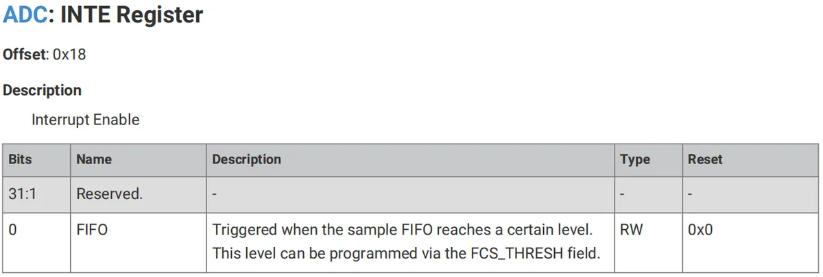
An interrupt can be generated when the number of samples in the FIFO reaches the configurable threshold FCS.THRESH. Note, however, that we need to first enable the interrupt via the INTE register's FIFO data bit:
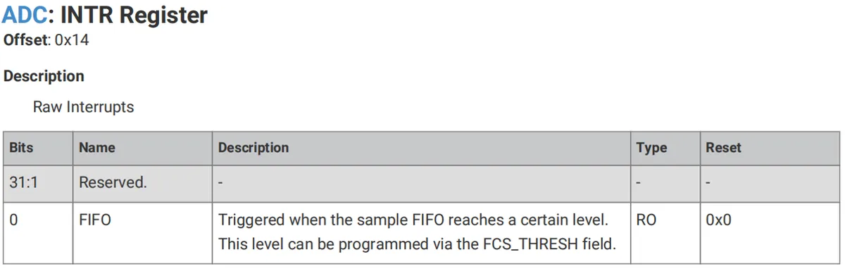
The interrupt status can be read from the INTS register. The interrupt is cleared by reducing the number of samples in the FIFO to below the sample threshold set by FCS.THRESH:
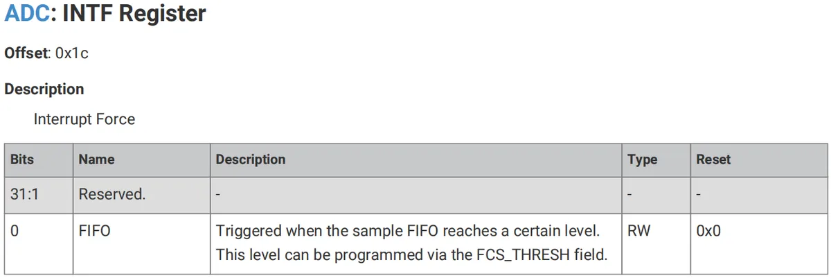
We can manually trigger the ADC interrupt via the INTF register: setting the corresponding bit to 1 will forcibly trigger the interrupt without waiting for the number of samples in the FIFO to reach the threshold.
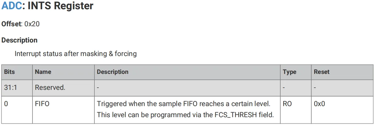
We can read the interrupt trigger status after interrupt masking and forcing operations via the INTS register:
1.3.5 Effective Accuracy of ADC
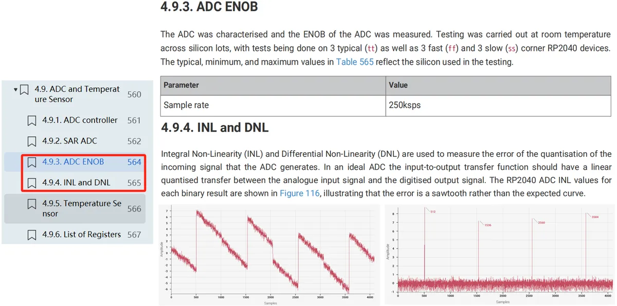
Here, the datasheet also mentions the test on the ADC accuracy of the RP2040, during which its Effective Number of Bits (ENOB) is measured. Simply put, three parameters of its ADC, namely ENOB (Effective Number of Bits), INL (Integral Non-Linearity) and DNL (Differential Non-Linearity), are tested. The specific content will not be elaborated here, and those in need can refer to the datasheet by themselves.
1.3.6 Built-in Temperature Sensor
The temperature sensor of the RP2040 microcontroller determines the temperature by measuring the base-emitter voltage (Vbe) of a biased bipolar diode. This sensor is connected to the fifth ADC channel (AINSEL= 4). Typically, Vbe is approximately 0.706 V at 27°C, and the relationship between temperature and voltage is as follows:
T = 27 - (ADC_voltage - 0.706) / 0.001721
Here, ADC_voltage represents the base-emitter voltage, which varies with temperature: for every 1°C increase in temperature, the Vbe voltage decreases by approximately 1.721 mV.
It should be noted that the temperature sensor is extremely sensitive to errors in the reference voltage. For example, if the reference voltage decreases by 1%(e. g., from 3.3V to 3.267V), the temperature corresponding to the same ADC value of 891 will change to 24.3°C. A mere 1% change in the reference voltage can result in a temperature error of more than 4°C. Therefore, to improve the accuracy of the internal temperature sensor, it is recommended to consider using an external reference voltage.
Prior to using the temperature sensor, it is necessary to first enable its bias power supply via the CS.TS_EN data bit, which will increase the current consumption on ADC_AVDD by approximately 40μA.
The temperature sensor of the RP2040 is suitable for basic temperature measurement, but for high-precision applications, the stability of the reference voltage needs to be considered, and calibration may be required to compensate for changes in Vbe and Vbe slope.
1.4 ADS1115 External ADC Chip
1.4.1 Introduction to the ADS1115 Chip
The ADS1115 is a high-precision, low-power 16-bit analog-to-digital converter (ADC) launched by Texas Instruments (TI). Integrated with multiple functions, it is suitable for a variety of analog signal acquisition and processing applications, such as sensor interfaces, voltage monitoring, and portable devices. The ADS1115 is usually connected to a microcontroller via the I²C interface; its circuit includes power supply pins (VDD, GND), SCL and SDA for I²C communication, an ADDR pin for setting the device address, and A0 to A3 as analog input pins.
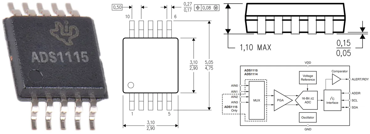
The main features are as follows:
- Resolution: 16-bit, delivering high-precision data conversion
- Programmable sampling rate: up to 860 samples per second (SPS), adjustable based on application requirements
- Input Configuration: The ADS1115 features an input multiplexer (MUX) that supports four single-ended inputs or two differential inputs
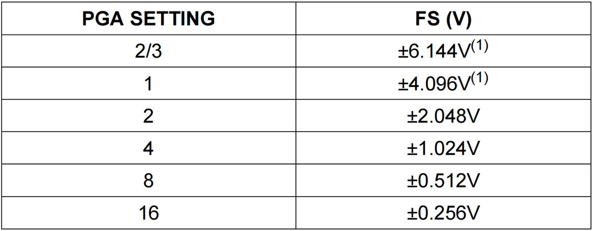
- Programmable Gain Amplifier (PGA): Built-in PGA with adjustable gain range (±6.144 V to ±0.256 V) to expand the measurable range of signals
- Interface: Standard I²C interface, supporting multi-device connection via address selection through the ADDR pin
- Low power consumption: The current consumption in continuous mode is approximately 150μA, while the single-conversion mode further reduces the current consumption during standby.
- Wide power supply range: It features a wide operating power supply range from 2.0V to 5.5V
- Internal Low-Drift Reference Voltage: Provides a stable reference voltage to ensure high-precision analog-to-digital conversion
- Internal Oscillator: Equipped with an internal oscillator, it eliminates the reliance on an external clock source.
1.4.2 Internal Structure and Pin Description of the ADS1115 Chip
The ADS1115 chip provides the following pins:
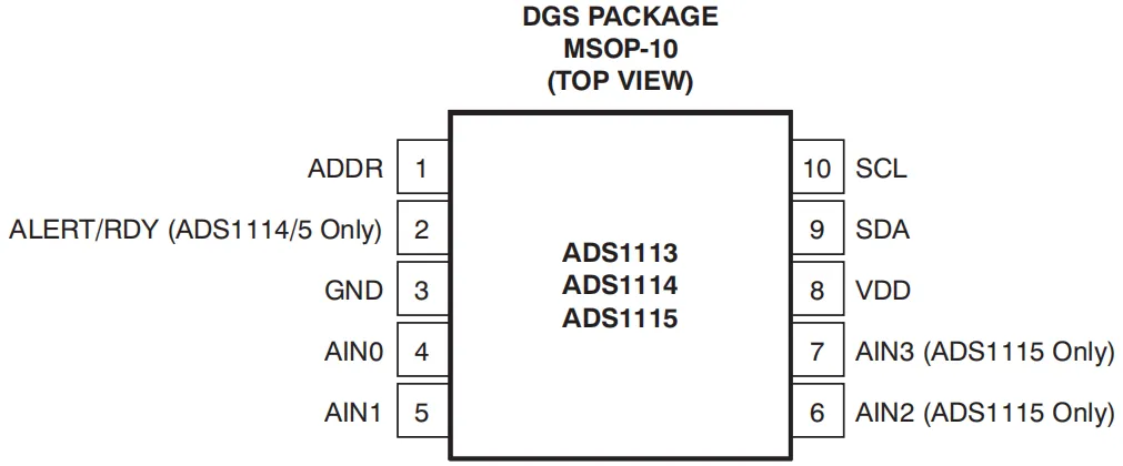
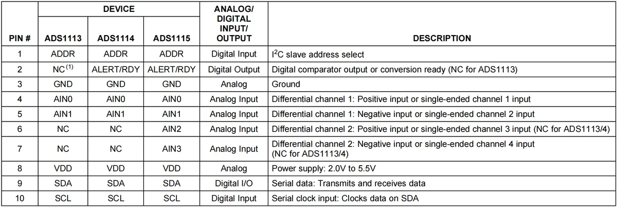
The functions of each pin are as follows:
- VDD (Power Pin): The supply voltage ranges from 2.0 V to 5.5 V, and the maximum operating current is 150 µA
- GND (Ground Pin): Connected to ground to provide a reference ground
- SCL (Serial Clock Pin): The clock line of the I²C interface, with input high voltage ranging from 0.7 × VDD to VDD + 0.3V, input low voltage ranging from 0V to 0.3 × VDD, supporting a communication rate of up to 400 kHz, and requiring an external pull-up resistor (typical value: 4.7kΩ)
- SDA (Serial Data Pin): it is the data line of the I²C interface; its electrical parameters are the same as those of SCL, and a pull-up resistor is also required for it.
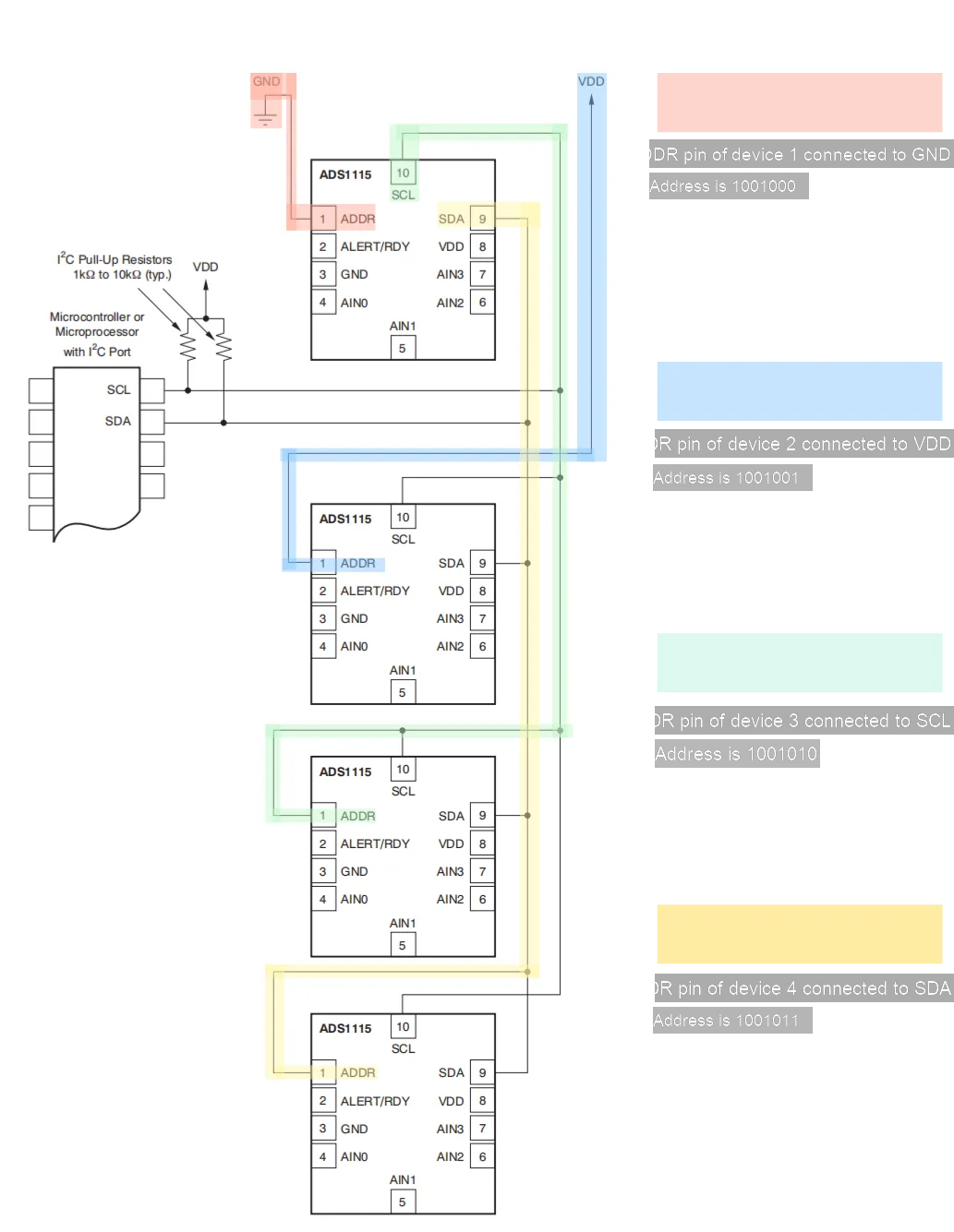
- ADDR (Address Select Pin): This pin is used to set the I²C address of the ADS1115; depending on the wiring configuration of this pin, 4 different I²C addresses are available.
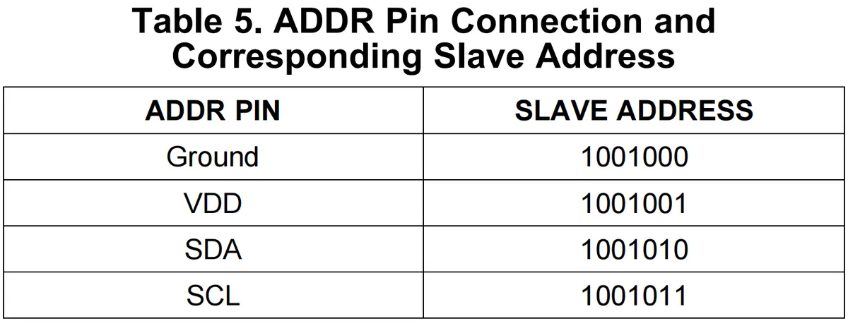
- ALERT/RDY (Interrupt/Ready Pin): This pin can be configured as a comparator interrupt pin or a signal indicator pin when data conversion is complete; it is an open-drain output and requires an external pull-up resistor.
- AIN0, AIN1, AIN2, AIN3 (Analog Input Channels): These are four analog input channels for single-ended or differential input. The input voltage must not exceed VDD + 0.3V or fall below GND - 0.3V, and the valid input voltage range is also related to the configuration of the PGA (Programmable Gain Amplifier).
The internal structure of the ADS1115 chip is as follows:
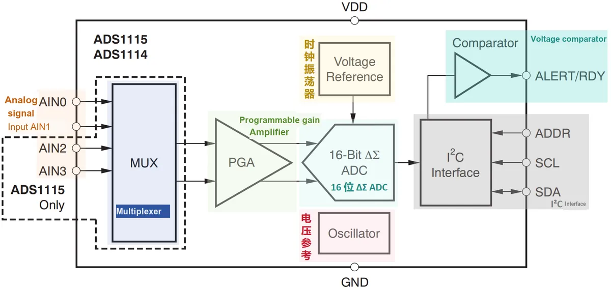
It includes the following units:
- MUX (Multiplexer): By configuring the multiplexer, we can select to use differential measurement or single-ended measurement for the four input channels (AIN0 to AIN3).
- PGA (Programmable Gain Amplifier): It amplifies the input signal and transmits it to the 16-bit ΔΣ ADC; its gain is configurable to adapt to input signals of different ranges.
- I²C interface: used for communication with an external MCU, it adopts standard SCL (clock) and SDA (data) signals, and the ADDR pin can be used to set the device address, which allows multiple ADS1115 chips to be connected to the same I²C bus
- Comparator Voltage Comparator: An optional comparator function that, in combination with the ALERT/RDY pin, can issue an interrupt signal when data is ready or a set threshold is reached.
- 16-bit ΔΣ ADC: Converts analog signals into 16-bit digital signals and transmits data via the I²C interface
- Internal Voltage Reference and Clock Oscillator: Provides a stable internal clock and voltage reference for accurate analog-to-digital conversion
1.4.2.1 Multiplexer
The ADS1115 has a built-in multiplexer (MUX), which allows us to select signals from multiple input channels for measurement. There are two main connection modes for input signals: differential input and single-ended input.
- Differential input: means that the signal is measured by the voltage difference between two input pins (positive input and negative input). For the ADS1115, this means it measures the voltage difference between
AINP(positive input) andAINN(negative input);Differential inputs can measure both positive and negative voltages, meaning the input range is±Vref, which is a full-scale (bipolar) range. The differential input mode can utilize the full resolution of the ADC, where all 16 bits can be used to resolve the signal. The full-scale range is divided into 2^16 = 65536 discrete values, and the resolution is2Vref / 65536 - Single-ended input: means that the signal is input from one channel while the other channel is grounded (usually connected to
GND), and the ADC actually measures the voltage of the input signal relative to the ground; the measurement range of single-ended input is from 0 toVref, which means it can only measure positive voltages and cannot measure negative voltages, and the effective input range of the signal becomes unipolar. The single-ended input mode only uses 15 bits of it, resulting in a 1-bit loss of resolution. The full-scale range is 2^15 = 32768 discrete values, and the resolution becomesVref / 32768
A multiplexer (MUX) is an electronic switching device that selects one from multiple signal sources to serve as the output:
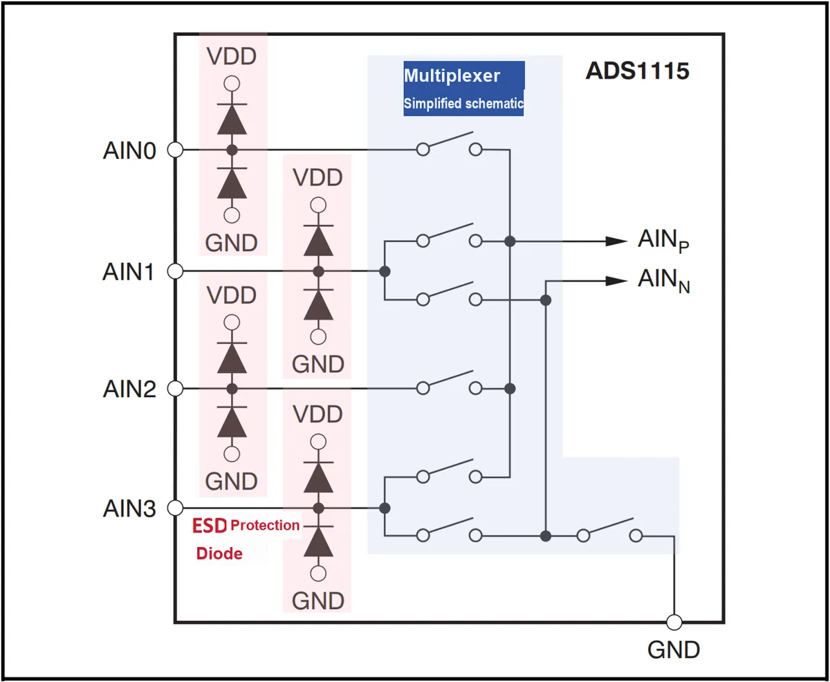
The ADS1115 allows selection of different input modes via the MUX bits in the configuration register; when measuring a single-ended signal, the MUX internally connects the negative input terminal (AINN) of the ADC to ground (GND).
The signal input channels of the ADS1115 are also equipped with electrostatic discharge (ESD) protection diodes, which are used to protect the ADC inputs from overvoltage or negative voltage. To prevent these ESD diodes from turning on, the voltage of the input signal must be maintained within the following range:
GND - 0.3V < AINx < VDD + 0.3V
If the input signal is likely to exceed this range, it is recommended to use an external Schottky diode or a series resistor to limit the input current so as to protect the ADC. Meanwhile, when using the ADS1115, if some input channels are not connected to signals and may be "overdriven"(i. e., the input voltage exceeds the valid range), the conversion results of other channels may be affected. It is suggested to provide voltage clamping (e. g., via a Schottky diode) for these unused input channels to avoid impacts on the measurement.
1.4.2.2 Analog Signal Input
The ADS1115 employs a switched-capacitor architecture to measure differential voltages, a structure that relies on the timing of the closing and opening of switches (S1 and S2) to charge and discharge the input capacitor:
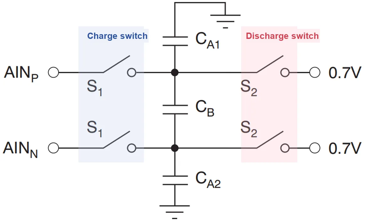
Wherein, S1 is a charging switch, and S2 is a discharging switch: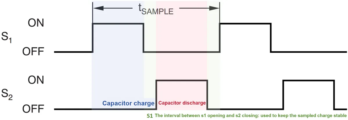
- S1 Charging Switch: S1 controls the sampling of external signals by the capacitor from the input terminals AINp and AINn. When S1 is closed, the capacitor charges and is charged to the voltages of AINp and AINn; when S1 is open, the capacitor holds the sampled voltage and prepares for discharging in the next stage.
- S2 Discharge Switch: S2 closes after S1 is turned off to initiate the discharge process; at this point, the charge in the capacitor is discharged to the reference voltage (typically 0.7V or 0V), and the purpose of this process is to prepare for the next sampling cycle.
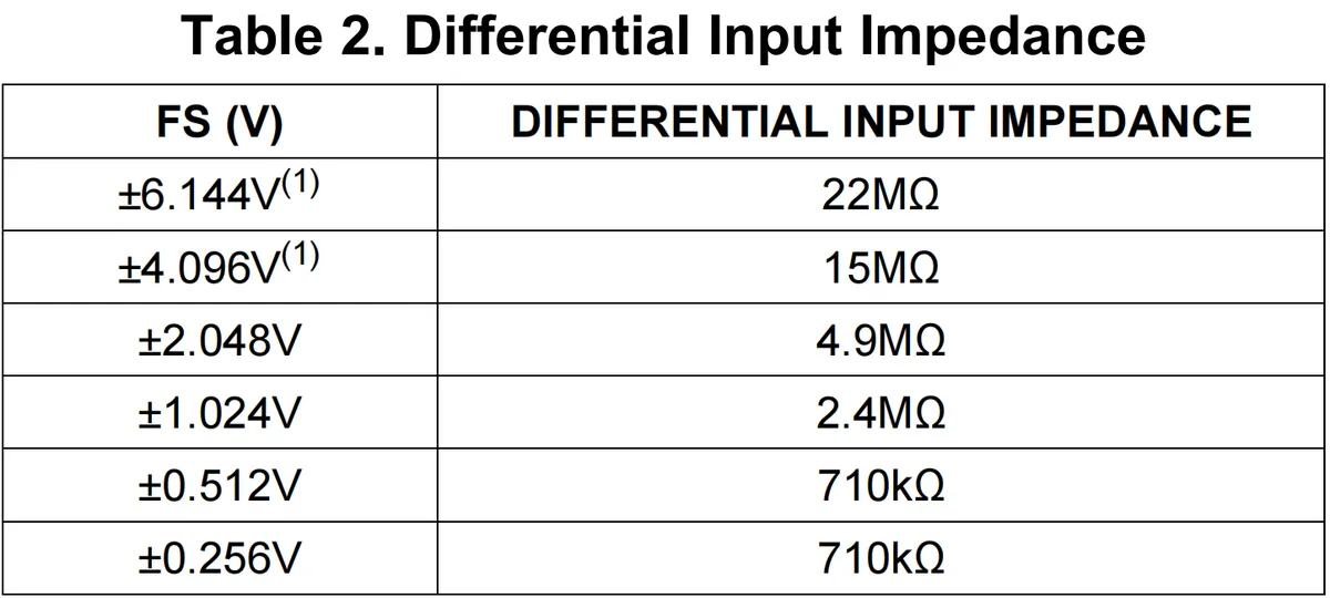
Since the charging and discharging of capacitors will induce transient currents, which are very small, their average value can be used to calculate the effective input impedance of the ADC:
whereis the input voltage, andis the average current. When the built-in PGA of the ADS1115 uses different gains, the full-scale range of the ADS1115's ADC varies, and its input impedance also differs accordingly:
1.4.2.3 PGA Programmable Gain Amplifier
PGA is an amplifier whose amplification factor can be dynamically adjusted via an external control signal; it can dynamically adjust the gain according to different input voltages to ensure that the signal fits the input voltage range of the ADC.
The internal structure of PGA mainly consists of the following components: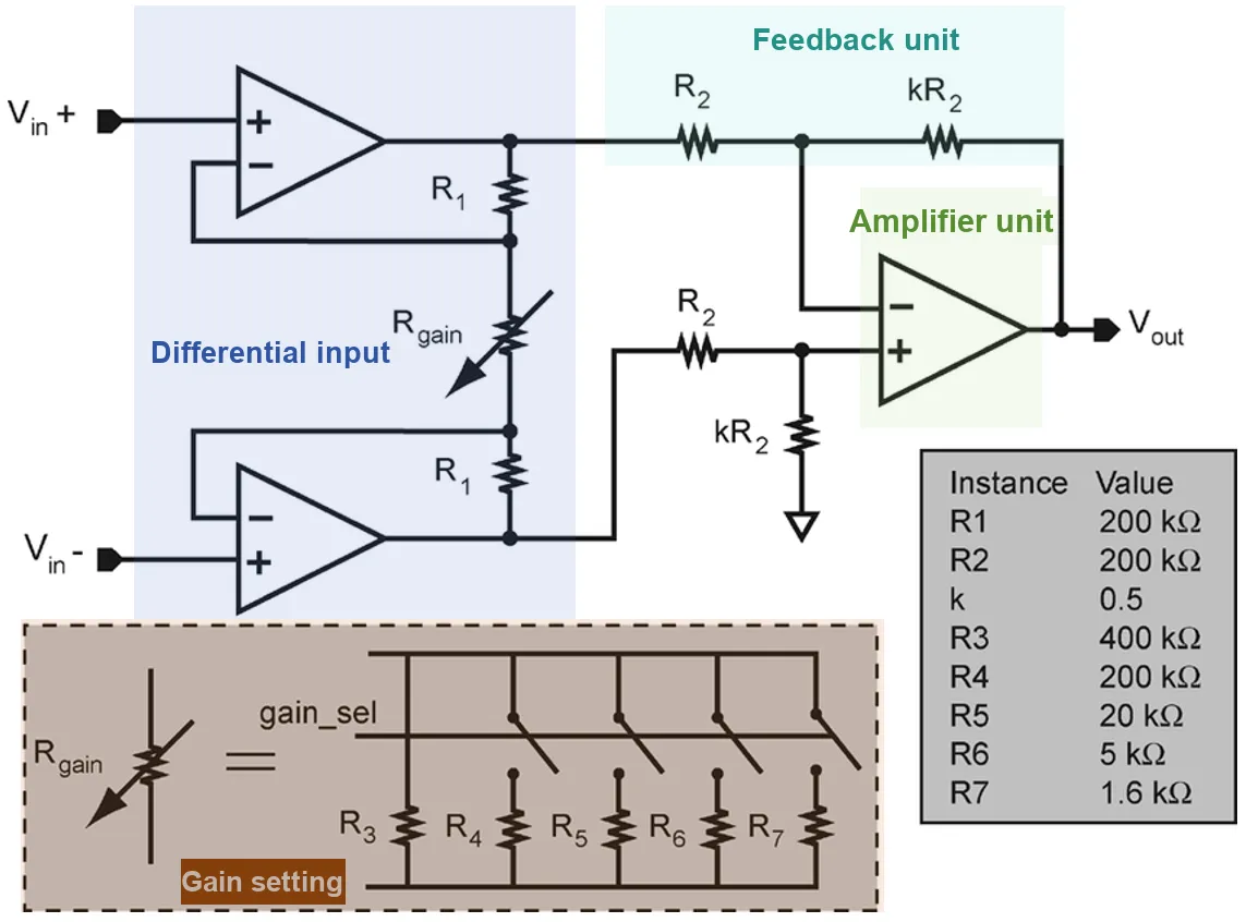
- Gain control circuit: A gain control circuit typically consists of a set of resistor networks, which select different gain settings via a switch matrix; different resistance values in the resistor networks can adjust the amplification factor of the input signal.
- Feedback circuit: A PGA relies on feedback control to ensure the stability of the amplifier. By adjusting the feedback resistor, the PGA can control the amplification factor of the output.
- Differential Input and Output: A PGA typically adopts differential input (with two input terminals: a non-inverting input and an inverting input) to mitigate noise interference and common-mode signals.
- Amplifier Core: This section refers to the operational amplifier, which is responsible for actual signal amplification. The op-amp receives the input signal from the gain control circuit and outputs an amplified signal according to the selected gain multiplier.
Next, we illustrate the function of PGA and its impact on the input signal range through an example. Suppose we are measuring the output of a sensor whose output analog signal fluctuates around 0.001V, while the measurement range of the ADC in use is 0~5V with a resolution of 10 bits. In this case, each digital step (minimum change) is 5V/1024 = 0.00488V. After ADC conversion, the calculated digital signal will always be 0, and we cannot effectively detect the tiny changes of the sensor via the ADC.
To improve the signal detection capability, we introduce a PGA to amplify the input signal by a factor of 100. At this point, the variation range of the input signal becomes 0.1 V. After amplification, the digital signal obtained after ADC conversion will range from 0 to 20, and we can observe the fluctuations of the input signal:
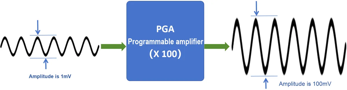
However, the use of a PGA also affects the range of the input signal. Since the amplification factor of the PGA is 100 at this time, the signal input range is also reduced by a factor of 100, and the original input range of the ADC (0~5V) will become 0~0.05V. If we try to input a signal higher than 0.05V (for example, 0.1V), it will exceed the input range of the PGA, which may lead to output saturation or distortion.
Selecting an appropriate PGA gain is critical to ensuring that the ADC can measure signals effectively. We need to ensure that the PGA gain setting boosts the input signal to the optimal measurement range of the ADC; generally, the input range of an ADC is from 0 to a certain reference voltage (e. g., 0 to 3.3V), so the amplitude of the input signal should be adjusted to fall within this range. At the same time, it is necessary to ensure that the PGA gain setting will not cause the output signal to exceed the maximum input voltage of the ADC (e. g., 3.3V).
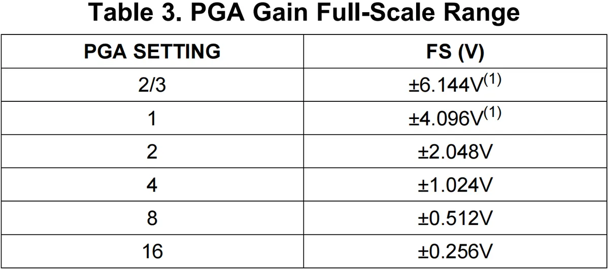
The ADS1115 incorporates a Programmable Gain Amplifier (PGA) to amplify input signals, and this PGA features multiple gain settings including 2/3,1, 2,4, 8 and 16; under different gain settings of the PGA, the full-scale input range varies, meaning the maximum analog input voltage range that the ADC can accept will change accordingly:
1.4.2.4 ADC Analog-to-Digital Conversion Unit
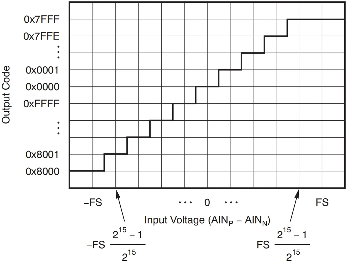
The ADS1115 stores the result of analog-to-digital conversion of analog signals in two's complement format: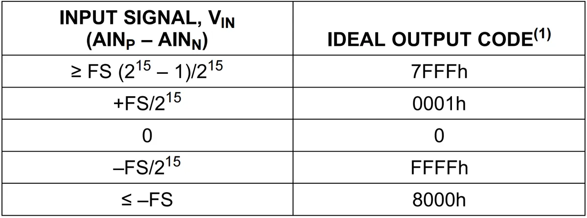
- When the input signal reaches the maximum positive value that can be stored, the value of the register corresponding to the ADC for storing the conversion result is
7FFFh, which is equivalent to 32767 in decimal. When the input signal exceeds the maximum positive value, the value stored in the ADC's corresponding conversion result register remains unchanged. - When the input signal reaches the minimum negative value that can be stored, the value of the ADC register corresponding to storing the conversion result is
8000h, which is equivalent to -32768 in decimal; when the input signal exceeds this minimum negative value, the value stored in the ADC register for the corresponding conversion result remains unchanged. - The minimum resolution of the ADS1115 is related to the PGA gain setting; when the PGA gain setting changes, the full-scale range will change accordingly.
The relationship between the input voltage and code conversion is shown as follows:
To prevent frequency-domain aliasing, the sampling rate of ADC data needs to be at least twice the frequency of the input signal. The digital filter built into the ADS1115 chip can attenuate high-frequency noise to a certain extent, but external filters may be required in some applications. Meanwhile, when designing an input filter circuit, the interaction between the filter network and the input impedance of the ADS1115 chip needs to be taken into consideration.
The ADC of the ADS1115 can operate in two modes: continuous conversion mode and single-shot conversion mode.
- Continuous Conversion Mode: In this mode, the ADS1115 chip continuously performs analog-to-digital conversions. After each conversion is completed, the conversion result is stored in the conversion register, and the next conversion starts immediately.
- Single-shot conversion mode: In single-shot conversion mode, the ADS1115 waits for the OS bit in the configuration register to be set to high level. Once the OS bit is set, a single analog-to-digital conversion is initiated, and meanwhile this bit is cleared to 0 to indicate that a conversion is in progress. Once the conversion data is ready, the OS bit will be set again, and the device will enter a low-power state.
1.4.2.5 Internal Voltage Comparator
The ADS1115 chip has a built-in voltage comparator, and the function of this comparator can be configured:
- Traditional Comparator: In this mode, the
ALERT/RDYpin is triggered when the converted data exceeds the limit set in the high threshold register (default: active low); the comparator releases the trigger when the input signal falls below the value in the low threshold register. - Window Comparator: In this mode, if the converted data exceeds the high threshold register or falls below the low threshold register,
the ALERT/RDYpin will be triggered.
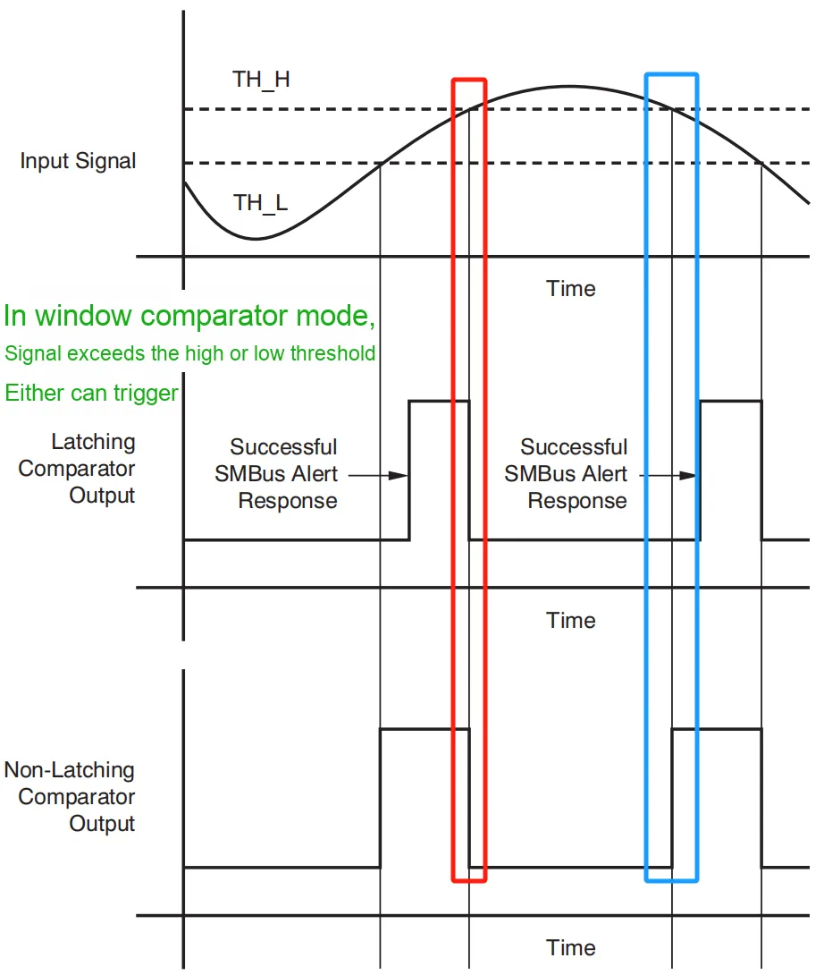
At the same time, this voltage comparator also features a COMP_LAT latch bit, which can be configured to keep the comparator active after triggering even if the input signal no longer exceeds the threshold; the COMP_POL polarity setting bit of the voltage comparator can configure the ALERT/RDY pin to be active high or active low.
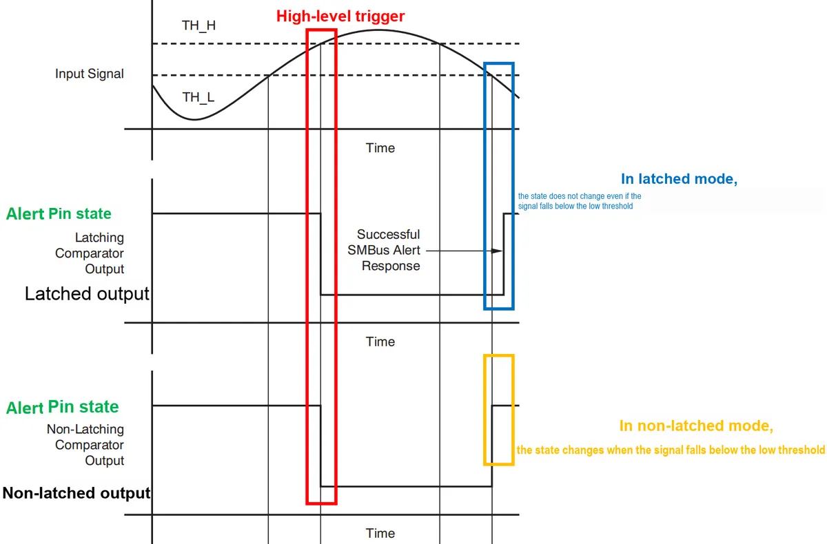
Meanwhile, the comparator can be configured to wait for a certain number of signal crossings above the threshold after the threshold is reached before triggering, the COMP_QUE bit can be set to wait for 1,2 or 4 read operations exceeding the threshold, and COMP_QUE can also disable the comparator function.
and ALERT/RDY pin. Depending on the register configuration, this pin can function either as an alarm pin or as a data-ready completion signal, as detailed in Section 1.4.4.4 Voltage Comparator Threshold Register.
1.4.2.6 Connection of ADS1115 Chip to Microcontroller
When using the ADS1115 to acquire external signals, the common connections are as follows:
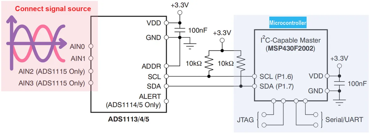
Among them, the VDD pin is externally connected to a filter capacitor to ensure stable power supply; the ADS1115 is connected to the microcontroller via the I2C interface, and at the same time ALERT pin also needs to be connected to a pull-up resistor.
Each ADS1113/4/5 can be configured with a unique I²C address via the address pin (ADDR), allowing up to four devices to be connected to the same bus:
1.4.4 Introduction to Registers of the ADS1115 Chip
The ADS1115 chip features the following registers:
- Pointer Register: Used to select the register to be accessed; by writing different values, the pointer register enables the main controller to access different registers.
- Config Register (Configuration Register): Configures the operating modes of the ADS1115, including input channel selection, gain setting, data rate, etc.
- Conversion Register: Used to store the result after internal ADC analog-to-digital conversion
- Lo_thresh and Hi_thresh Registers (Voltage Comparator Threshold Registers): used to set the thresholds of the internal voltage setting comparator.
The ADS1115 performs a reset upon power-up; during the reset process, the chip sets all bits in the configuration register to their respective default values.
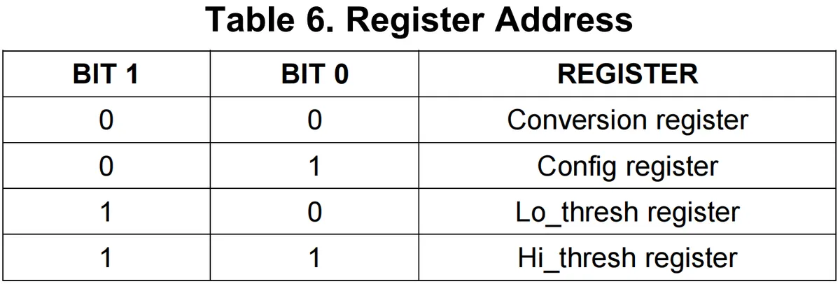
1.4.4.1 Pointer Register
Used to select the register to be accessed, the lower two data bits are writable:

By writing different values, the pointer register enables the main controller to access different registers:
1.4.4.2 Config Register (Configuration Register)
This register is readable and writable, and has 16 data bits:
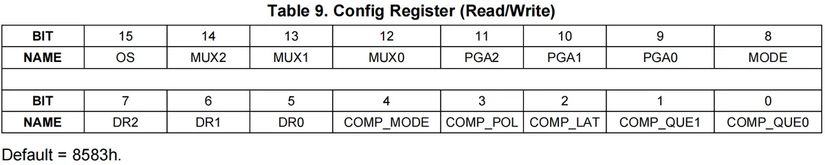
The meaning of each data bit is as follows:
data bit | Data Bit Name | Meaning |
15 | OS | Operation status / start of single conversion: This bit controls the operation status of the device and can only be written in shutdown mode. 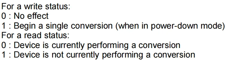 |
14-12 | MUX[2:0] | Input multiplexer configuration, used to select the input channel:  |
11-9 | PGA[2:0] | Programmable Gain Amplifier Configuration: The input voltage ranges for different configurations are as follows:  |
8 | MODE | Device operation mode control, with selectable options of single conversion mode or continuous conversion mode:  |
7-5 | DR[2:0] | Data Rate Control:  |
4 | COMP_MODE | Comparator mode control allows selection between a basic comparator (triggered by high/low level) or a window comparator:  |
3 | COMP_POL | Comparator polarity control, allowing selection of whether to output a high level or a low level after triggering: 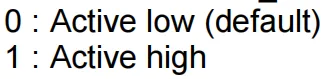 |
2 | COMP_LAT | Latch comparator control, which allows selection of whether to latch the current output level until the next state change:  |
1-0 | COMP_QUE | Number of consecutive threshold crossings beyond the upper and lower limits that must occur before the 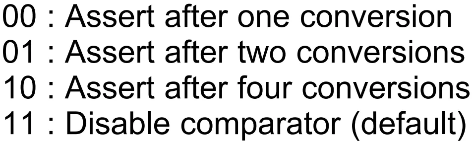 |
1.4.4.3 Conversion Register
The 16-bit conversion register holds the result converted by the ADC, stored in the form of two's complement; after power-on, the conversion register is cleared to 0 and remains at 0 until the first conversion is completed.

1.4.4.4 Lo_thresh and Hi_thresh Registers (Voltage Comparator Threshold Registers)
The Lo_thresh and Hi_thresh registers of the ADS1115 are used to set the thresholds for the comparator. These registers store the upper and lower threshold values of the comparator to determine whether the input signal exceeds the set range. When the voltage of the input signal exceeds the threshold, the device can send a signal through the ALERT/RDY pin:
Lo_threshregister stores the lower threshold of the comparator, and its value indicates that when the input signal voltage is lower than this threshold, the output of theALERT/RDYpin will be deasserted or triggered, depending on the current operating mode of the comparatorHi_threshregister stores the upper threshold of the comparator, and its value indicates that when the input signal voltage is higher than this threshold, it will trigger the output of theALERT/RDYpin- Under normal circumstances,
the value of the Hi_threshregister must be greater than the value stored in theLo_threshregister.
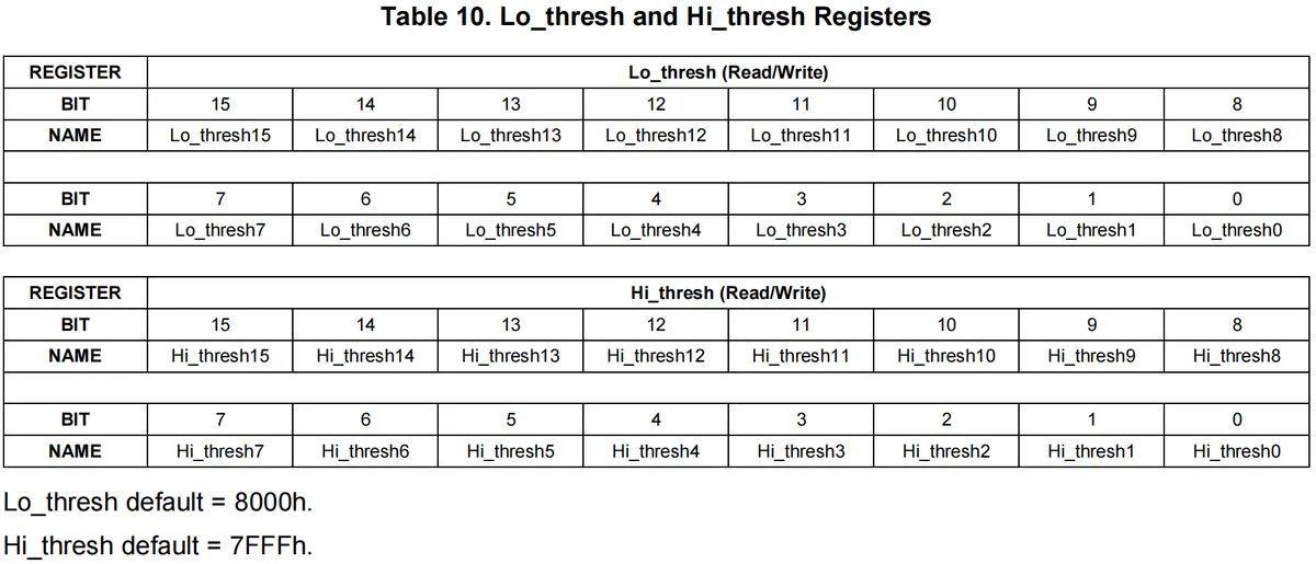
The values in these registers are stored in two's complement form: when the most significant bit (MSB, bit 15) is 0, it indicates a positive number; when the most significant bit is 1, it indicates a negative number.
Here, it should be noted that the ADS1115 integrates a programmable gain amplifier (PGA), which functions to set the maximum range of the input signal and ensure that the analog signal is properly amplified or attenuated before sampling. The full-scale input voltage range (FSR) can be adjusted between ±6.144V and ±0.256V; when the PGA gain setting is modified, the resolution of the device will change accordingly, so it is necessary to readjust the value of the threshold register after modifying the PGA setting.
For example:
- When the PGA is set to ±6.144 V, the voltage represented by 1 LSB is approximately 187.5 µV
- When the PGA is set to ±0.256V, the voltage represented by 1 LSB is approximately 7.8125µV
Under different PGA gain settings, Lo_thresh and Hi_thresh registers store values corresponding to different voltage ranges.
Here, the ADS1115 also provides an ALERT/RDY pin, which can function as either an alarm pin or a data ready signal depending on the register configuration.
- Alarm function: When the input signal voltage exceeds the range set by
Lo_threshorHi_thresh,the ALERT/RDYpin will send out an alarm signal. This function is similar to a voltage comparator. - Data preparation complete function (RDY mode): In single conversion mode, the
ALERT/RDYpin outputs theOSdata bit of the configuration register after each conversion is completed, indicating the completion of the conversion; in continuous conversion mode, theALERT/RDYpin emits a pulse when each conversion is completed. To achieve this function, simply set theMSBof theHi_threshregister to 1 and theMSBof theLo_threshregister to 0
1.4.5 I2C Communication Interface of the ADS1115 Chip
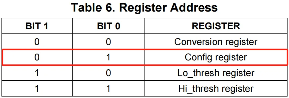
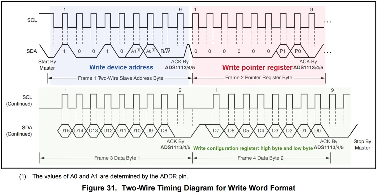
Taking setting the ADS1115 chip to continuous conversion mode as an example (assuming the chip address at this time is 0x48), first it is necessary to write the corresponding configuration value to the configuration register:
- The first byte: the I²C address of the slave device to be sent
0b1001000(0x48), plus a write operation bit0 - The second byte: points to the configuration register, i. e., sends
0b00000001(0x01) to the pointer register; this byte instructs the ADS1115 chip that the subsequent data to be written is the configuration register
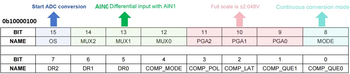
- The third byte: the MSB (most significant byte, upper 8 bits) of the configuration register, for example
0b10000100(0x84), this byte sets several key operating modes of the ADS1113/4/5
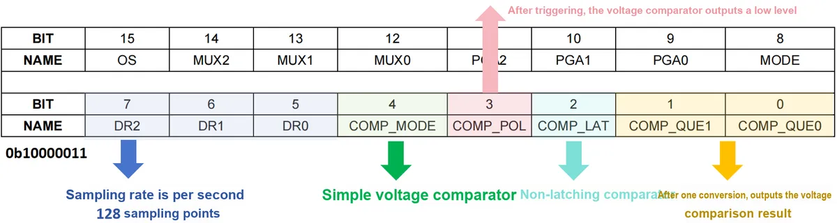
- Fourth byte: the LSB part (lower 8 bits) of the configuration register, for example
0b10000011(0x83), this byte contains the settings of the programmable gain amplifier (PGA), data rate, etc.
Here, both the pointer register and the configuration register are subjected to write operations, and the I2C write format of the ADS1115 chip is as follows:
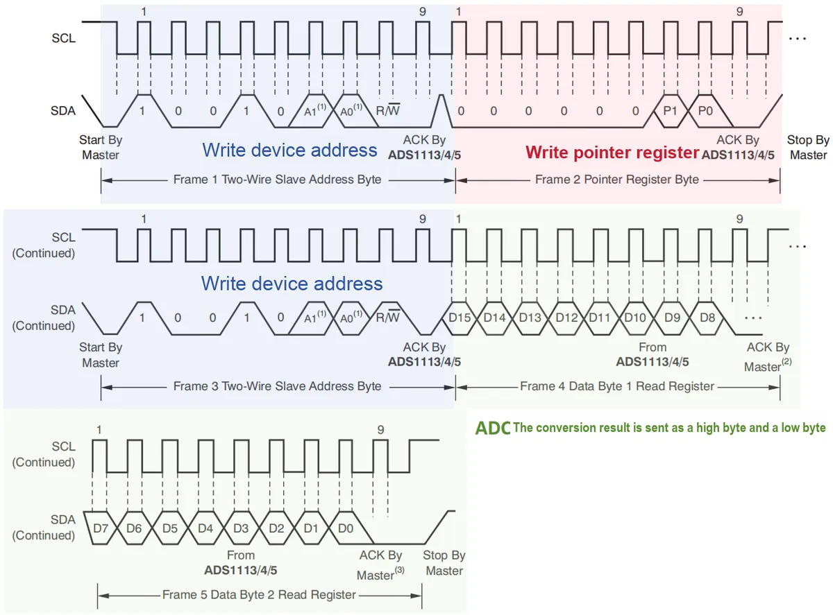
After the configuration is complete, we need to read the result after each ADC conversion. At this point, we first need to set the pointer register:
- The first byte: the I²C address of the slave device to be sent
0b1001000(0x48), plus a write operation bit0 - Second byte: send
0b00000000(0x00) to the pointer register to point to the conversion register
Then read the conversion result:
- First byte: the I²C address of the slave device to be sent
0b1001000and a read operation bit1, which is0b10010001 - The second byte: The ADS1113/4/5 device will transmit the upper 8 bits (MSB) of the conversion register
- Third byte: The ADS1113/4/5 device will transmit the lower 8 bits (LSB) of the conversion register
The process of reading the ADC conversion result is shown in the following figure:
2. Software Control Method
2.1 Constructor of the machine.ADC class
machine.ADC The constructor of the class is as follows:
machine.ADC(id, *, sample_ns, atten)
Construct an ADC object with the given parameters
The parameters are defined as follows:
- id: Specifies the instance ID of the ADC. It can be an integer (usually specifying the channel number), a
Pinobject, or other values supported by the underlying hardware. - sample_ns: Sampling time, in nanoseconds, which determines the duration for which the ADC acquires the analog signal. This parameter is not available on the Raspberry Pi Pico and is not supported in MicroPython v1.23.0.
- atten: Specifies the input attenuation, which affects how the input signal is processed. This parameter is not available on the Raspberry Pi Pico and is not supported in MicroPython v1.23.0.
2.2 Other methods of the machine.ADC class
The machine.ADC class has other methods as well:
Method | Description |
ADC.init(*, sample_ns, atten) | This method applies the given settings to the ADC object, and only the specified parameters will be changed; the sampling time and input attenuation parameters can be adjusted as required. |
ADC.block() | This method returns the Raspberry Pi Pico is not supported in MicroPython v1.23.0. |
ADC.read_u16() | This method performs a simulated read and returns an integer in the range of 0 to 65535. The returned value represents the raw value collected by the ADC, and these values are scaled to ensure that the minimum value is 0 and the maximum value is 65535. The actual voltage value is value/65535*3.3V. |
ADC.read_uv() | This method performs a simulated read and returns an integer value in microvolts (μV). Raspberry Pi Pico is not supported in MicroPython v1.23.0. |
The point that needs attention here is:
- When using the ADC peripheral of Raspberry Pi Pico, only integer IDs (i. e., ADC channel numbers) can be used in the constructor method.
- In the ADC class of the Raspberry Pi Pico, there is a
CORE_TEMPattribute that is used to specify the particular ADC channel for accessing the built-in temperature sensor:

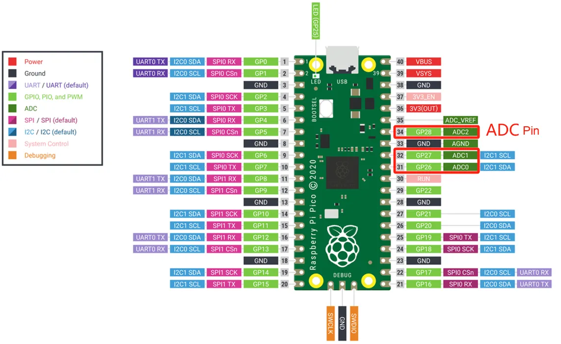
There are three ADC pins available for analog input on the Raspberry Pi Pico, which are as follows:
- GP26 (ADC0): Physical Pin 31
- GP27 (ADC1): Physical Pin 32
- GP28 (ADC2): Physical Pin 34
The ADC pins of the Raspberry Pi Pico can read analog voltages between 0 and 3.3V, and convert them into 16-bit digital values (ranging from 0 to 65535); these pins can be used to read signals from analog sensors such as potentiometers and photoresistors.
3. Application Examples
3.1 Periodically collect data from the internal temperature sensor
3.1.1 Example of Periodic Sampling of Internal Temperature Sensor
In the following code, we use a timer of MicroPython to periodically collect data from the internal temperature sensor and print it out in the main program.
The following code can be found in the material package we provide, at the elegance-devkit v1\Demo\57 ADC_Temp folder.
The sample program is as follows:
# Python env   : MicroPython v1.23.0
# -*- coding: utf-8 -*-
# @Time    : 2024/8/26 10:31 AM
# @Author  : Li Qingshui
# @File    : main.py
# @Description : ADC experiment, periodically sampling internal temperature sensor data

# ======================================== Import Modules ========================================

# Import the hardware module
from machine import ADC, Timer
# Import time-related modules
import time
# Import the deque (double-ended queue)
from collections import deque
# Import the module for accessing and controlling MicroPython internals
import micropython

# ======================================== Global Variables ============================================

# Voltage conversion factor
conversion_factor = 3.3 / (65535)
# Create an empty deque object to store temperature data
# temperature_list is the iterable used to initialize the deque
temperature_list = []
# 10 is the maximum length of the deque, 1 is the flags parameter, meaning overflow checking is enabled
temperature_deque = deque(temperature_list, 10, 1)
# Mark the start time
start_time = time.ticks_ms()

# ======================================== Functions ============================================

# Timer callback function
def timer_callback(timer: Timer) -> None:
    """
    Callback function that periodically samples internal temperature sensor data.

    Args:
        timer (machine.Timer): Timer object.

    Returns:
        None
    """
    # Use micropython.schedule to solve the dynamic memory allocation problem
    micropython.schedule(collect_temperature, 0)

# Function to sample temperature data
def collect_temperature(t: int) -> None:
    """
    The function that actually samples the temperature data.

    Args:
        t (int): Unused; only required to satisfy the micropython.schedule function signature.

    Returns:
        None
    """
    # Declare global variables
    global sensor_temp, temperature_deque, conversion_factor, start_time

    # Get the current time
    current_time = time.ticks_ms()
    # Calculate the sampling interval
    time_interval = time.ticks_diff(current_time, start_time)
    # Print the interval
    print("Time interval: {}ms".format(time_interval))

    # Read the raw data from the temperature sensor
    reading = sensor_temp.read_u16() * conversion_factor
    # Calculate the temperature (in degrees Celsius)
    temperature = 27 - (reading - 0.706) / 0.001721
    # Put the temperature data into the deque
    temperature_deque.append(temperature)

# ======================================== Custom Classes ============================================

# ======================================== Initialization ==========================================

# Power-on delay
time.sleep(3)
# Print debug information
print("FreakStudio : Get internal temperature data regularly")

# Initialize the internal temperature sensor
sensor_temp = ADC(4)
# Initialize the timer to sample data every 3 seconds
timer = Timer(-1)
timer.init(period=3000, mode=Timer.PERIODIC, callback= timer_callback)

# ========================================  Main Program  ===========================================

# Main program loop
while True:

    # When the ADC has collected new data
    if len(temperature_deque) > 0:
        # Get and print the latest temperature data from the deque
        # At this point temperature_deque is a FIFO (first-in, first-out) queue
        temperature = temperature_deque.popleft()
        # Print the temperature data
        print("Temperature: {:.2f}°C".format(temperature))

    # The main program checks the queue once per second
    time.sleep(1)
Here, we have carried out the following work:
- Regular temperature data collection: initialize the timer
timeras a periodic timer, which invokes thetimer_callbackfunction every 3 seconds; within thetimer_callbackfunction, themicropython.schedulefunction is used to execute thecollect_temperaturefunction, where the actual data acquisition and processing are completed in thecollect_temperaturefunction, and the collected and converted temperature data is inserted into thetemperature_dequequeue - The main program prints temperature data: The main program checks the deque once per second in a loop; if there is data in the deque, it retrieves the latest temperature data from the deque and prints it out
The following points require attention:
- Use
micropython.scheduleto perform data processing: In MicroPython, timer callbacks usually run for a very short time. If the operations inside a callback are complex or time-consuming, they may block the system. By usingmicropython.schedulefunction, the actual execution work can be deferred to run as soon as possible in the main program context;Meanwhile, memory allocation is prohibited in interrupt callbacks (you cannot create Python objects such as lists and queues in interrupts, nor perform insertion operations or floating-point operations),the micropython.schedulefunction can safely perform memory allocation in the main program without affecting the stability and speed of interrupts - Use
collections.deque(a double-ended queue) to store and read data:dequeis a first-in-first-out (FIFO) data structure, which is ideal for storing temperature data that changes over time. Each new temperature data entry is added to the end of the queue, while the oldest temperature data is removed from the front of the queue, allowing us to obtain a time-ordered sequence of temperature values. - Create a
collections.dequedeque object in MicroPython: Unlike creating a deque object in CPython on a host computer, there are certain restrictions here, which are related to the design goals of MicroPython (embedded systems and resource-constrained environments)
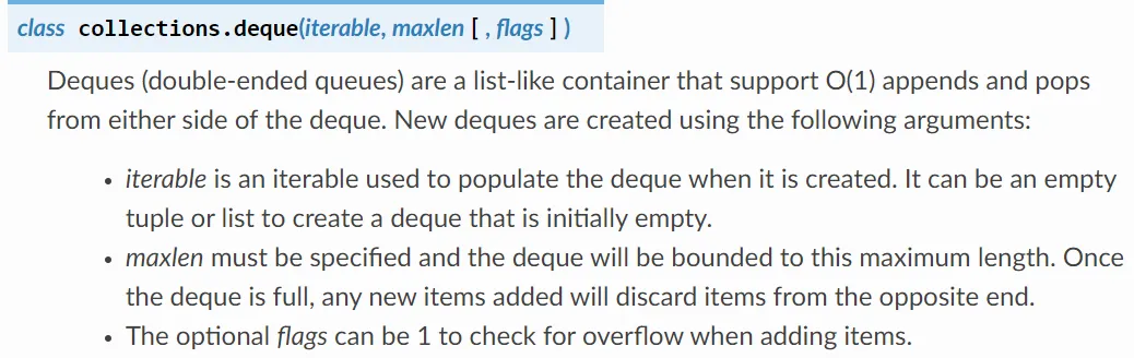
- An iterable object for initializing the queue must be passed in, and a list is commonly used for this purpose here.
- The maximum length of the queue must be set
maxlenvalue - The
flagsparameter can be set to control the queue overflow check:flags= 1Enables overflow checking. When attempting to add a new element, anIndexError will be raised if the queue is full.- If you do not need overflow checking, you can set it to 0
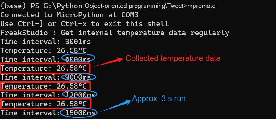
Burn the code, connect to the remote terminal, and the output is as follows:
3.1 Application Experiment.mp4 3.7 MB
It can be seen that the temperature data can be successfully collected at regular intervals and printed out.
3.1.2 Notes on MicroPython Interrupt Callback function
In the interrupt callback function of MicroPython, the following information needs to be noted:
- Keep the code as short and simple as possible: When an ISR is executed, it interrupts the running of the main program. Overly long or complex ISR code will cause the main program to be unable to resume execution for a long time, which may lead to system instability or response delays;ISR code should only complete the tasks that must be executed immediately after an interrupt event occurs. Operations that can be postponed should be delegated to the main program loop for processing. Generally, the function of an ISR is to handle the hardware device that triggered the interrupt and prepare it for the next interrupt, the ISR communicates with the main loop by updating shared data to indicate that an interrupt has occurred, and returns to the main loop as soon as possible
- Avoid memory allocation, do not append to lists or insert into dictionaries in ISRs, and do not use floating-point arithmetic: Performing dynamic memory allocation or complex computations (such as floating-point operations) in an ISR may trigger the garbage collector (GC), causing system stalls or even crashes; there is no guarantee that an ISR will have sufficient resources to safely complete these operations during execution, so any form of dynamic memory allocation or complex computation in ISRs should be avoided
- Consider using
micropython.scheduleto work around the aforementioned limitation:micropython.scheduleallows offloading heavier tasks to the main program for execution instead of handling them directly in the ISR; this approach bypasses the memory allocation restrictions in ISRs and reduces ISR execution time. - When an ISR returns multiple bytes, use a pre-allocated
bytearray; if multiple integers need to be shared between the ISR and the main program, consider usingarray.array: a pre-allocatedbytearrayorarray.arrayavoids dynamic memory allocation in the ISR while providing sufficient space to store and share data - When the main program accesses data shared with the ISR, consider disabling interrupts before accessing the data and re-enabling them immediately afterward (see Critical Section): The ISR and the main program may access the same data simultaneously, leading to a data race problem. By disabling interrupts when accessing shared data, you can prevent the ISR from preempting the main program while it is manipulating the shared data, thus avoiding data inconsistency or corruption. Restoring interrupts immediately after the access is completed ensures that the system does not miss important interrupt events.
- Allocate Emergency Exception Buffer: In the ISR, if an exception occurs and there is insufficient memory to store the exception information, the exception may be ignored. Allocating an emergency exception buffer ensures that the exception information can be stored and output even under memory-constrained conditions, helping developers identify and resolve issues during debugging.
These recommendations aim to maximize the efficiency and reliability of ISR, ensuring that embedded systems can operate stably and respond quickly when processing interrupts.
3.1.2.1 Limitations of MicroPython Interrupt Callback Function
In MicroPython, there is a special relationship between interrupt handling and the garbage collector (gc), which is mainly reflected in the restrictions on memory allocation. Specifically:
- Locking of the Garbage Collector: When the garbage collector is running, MicroPython locks the memory allocation process to ensure the security of memory management. This means that while the garbage collector is active, the program cannot perform dynamic memory allocation operations. This is particularly critical for Interrupt Service Routines (ISRs), as they may be triggered at virtually any point during program execution.
- Memory Allocation Restrictions in ISRs: Since interrupts can be triggered at any time, including when the garbage collector is running, MicroPython has a constraint in place: dynamic memory allocation is not permitted within ISRs, which is intended to avoid potential issues caused by the garbage collector locking memory allocation during ISR execution. If an attempt is made to allocate memory in an ISR while the garbage collector happens to have locked memory allocation, the program may throw an exception or even crash.
- Pre-allocate memory: To avoid this issue, developers need to allocate all required memory resources before the ISR is triggered. This means that all data structures, objects and memory blocks for the ISR should be pre-allocated in the main program and used directly in the ISR, rather than dynamically creating new objects or allocating new memory within the ISR.
Here, we also cannot perform floating-point arithmetic, because floating-point numbers are Python objects, and creating a floating-point number requires memory allocation, which is prohibited in an ISR; similarly, an ISR cannot append elements to a list (append) because this would involve memory allocation.
3.1.2.2 MicroPython Emergency Exception Buffer
In MicroPython, developers can pre-allocate a certain amount of memory to store exception information that occurs in Interrupt Service Routines (ISRs), including traceback details. This approach allows, when a problem is encountered in an ISR, the exception information to be saved in the pre-allocated buffer and later output to the REPL (Read-Eval-Print Loop) terminal at an appropriate time, helping developers debug and resolve issues.
This is done by adding the following code at the top of main.py or boot.py:
import micropython
micropython.alloc_emergency_exception_buf(100)
The above code pre-allocates a 100-byte buffer for storing exception information that may be thrown in the ISR, and the MicroPython documentation recommends 100 bytes as an appropriate buffer size. However, the emergency exception buffer can only store the stack trace information of one exception. This means that if another exception is thrown again while processing the first exception, the stack trace information of the second exception will overwrite the previously stored stack trace information of the first exception. This may prevent developers from obtaining accurate information about the first exception during debugging, leading to confusion and misguidance.
3.1.2.3 Communication Between ISR and Main Program
Communication between an ISR (Interrupt Service Routine) and the main program usually needs to be implemented via shared data objects. The simplest approach is to use global variables or share these data objects via classes. Common shared data objects include integers, bytes, bytearrays, as well as arrays that can store various data types (the array object in the array module). This method allows the ISR to quickly pass status or data to the main program after processing an interrupt event, so that the main program can make corresponding responses.
3.1.2.4 Using Object Methods as Callback Functions
Using object methods as callback functions is a powerful technique, which is supported by MicroPython. This feature allows ISRs (Interrupt Service Routines) to share data with instance variables; not only does this approach enable classes to implement drivers for multiple device instances, but it also makes it easy to access and update the state of instances within ISRs.
The following example makes two LEDs blink at different rates:
import pyb, micropython
micropython.alloc_emergency_exception_buf(100)

class Foo(object):
    def __init__(self, timer, led):
        self.led = led
        timer.callback(self.cb)

    def cb(self, tim):
        self.led.toggle()

# Create two instances, each associated with a different timer and LED
red = Foo(pyb.Timer(4, freq=1), pyb.LED(1))
green = Foo(pyb.Timer(2, freq=0.8), pyb.LED(2))
In this example, the Foo class's cb method is an instance method, which is set as the callback function of the timer. Whenever the timer triggers an interrupt, the cb method of the corresponding instance will be invoked:
- When timer 4 triggers an interrupt,
redinstance'scbmethod will be called, thereby toggling the state of LED 1 (turning it on or off). - Similarly, when timer 2 triggers an interrupt,
greeninstance'scbmethod will be called, which toggles the state of LED 2
One major benefit of this design is that it allows the same class Foo to be used to control multiple hardware instances; in this example, the Foo class can manage both timer 4 and timer 2 along with their corresponding LEDs simultaneously. Since cb is a bound method, its first parameter is self, which enables the callback function to access the instance variables of the class. For instance, if there is a Foo class constructor has a self.count variable, the cb method can increment this counter each time it is invoked.This means that red and green instances can maintain independent LED state switching counts respectively.
By using object methods as callbacks, multiple hardware instances can share the same code, which reduces the amount of code and improves its maintainability.
3.1.2.5 Indirect "Creation" of Python Objects in ISR
In MicroPython, an ISR (Interrupt Service Routine) cannot create Python objects. This is because MicroPython needs to allocate memory for objects from a free memory block storage called the heap. However, heap memory allocation is not allowed in interrupt handlers, as heap allocation is not reentrant. In other words, an interrupt may occur while the main program is executing a memory allocation; to maintain the integrity of the heap, the interpreter prohibits memory allocation within ISR code.
We have the following several solutions to address this problem indirectly:
- Pre-allocated buffer: One way to avoid this issue is to use a pre-allocated buffer in the ISR; for example, the class constructor can create a
bytearrayinstance and a boolean flag. The ISR method can assign data to a specific position in the buffer and set the flag. In this way, memory allocation occurs when the object is instantiated in the main program code, rather than in the ISR. The sample code is shown below, where the class constructor pre-allocates abytearrayinstance and uses it in the ISR:
import pyb

class SensorReader:
    def __init__(self):
        # Pre-allocate a buffer to store data
        self.buffer = bytearray(3)
        self.data_ready = False  # Boolean flag indicating whether the data is ready

    def read_sensor(self):
        # Simulate reading sensor data and storing it in the buffer
        self.buffer[0] = 0x01  # Assumed sensor data
        self.buffer[1] = 0x02
        self.buffer[2] = 0x03
        self.data_ready = True  # Set the flag to indicate the data is ready

    def get_data(self):
        if self.data_ready:
            return self.buffer
        return None

# Create an instance
sensor = SensorReader()

# ISR example
def timer_callback(timer):
    sensor.read_sensor()  # Use the pre-allocated buffer in the ISR

# Set up the timer to call the ISR every 2 seconds
tim = pyb.Timer(4, freq=0.5)
tim.callback(timer_callback)

# Main program loop
while True:
    data = sensor.get_data()
    if data:
        print("Sensor data:", list(data))
pyb.delay(1000)- I/O Methods in the MicroPython Library: The I/O methods of the MicroPython library usually provide the option of using a pre-allocated buffer. For example,
pyb.i2c.recv ()can accept a mutable buffer as its first argument, which makes it usable within an ISR.
import pyb

# Initialize I2C
i2c = pyb.I2C(1, pyb.I2C.MASTER, baudrate=100000)

# Pre-allocate a buffer
buffer = bytearray(10)

def i2c_callback(timer):
    i2c.recv(buffer, addr=0x42)  # Use the pre-allocated buffer in the ISR

# Set up the timer to call the ISR every 1 second
tim = pyb.Timer(4, freq=1)
tim.callback(i2c_callback)

# Main program loop
while True:
    print("Received I2C data:", list(buffer))
pyb.delay(1000)- Create an object with default parameters: Without using classes or global variables, objects can be created via default parameters, which avoids memory allocation in ISRs.
def set_volume(t, buf=bytearray(3)):
    buf[0] = 0xa5
    buf[1] = t >> 4
    buf[2] = 0x5a
    return buf

# Example usage
volume_data = set_volume(10)
print("Volume data:", list(volume_data))- Reference binding method: Passing a reference to a bound method directly in a MicroPython ISR will cause memory allocation issues, as dynamic memory allocation is not permitted within an ISR. Below is a counterexample that demonstrates the errors that may arise from directly passing a reference to a bound method in an ISR.
import pyb

class Foo:
    def __init__(self):
        self.x = 0.1
        tim = pyb.Timer(4)
        tim.init(freq=2)
        tim.callback(self.cb)

    def cb(self, t):
        self.x *= 1.2
        print(self.x)

foo_instance = Foo()
In the code above, tim.callback (self.cb) directly passes self.cb (a bound method) to the timer's callback function. When the timer triggers an interrupt, MicroPython will attempt to execute this callback function. However, self.cb is a reference to a bound method, and when invoking this bound method, MicroPython needs to allocate memory on the heap to handle the context of this call (i. e., the self bound to the instance).Since memory allocation is prohibited in ISRs, this operation of directly passing a reference to a bound method may cause errors and even crash the system.
To avoid directly passing a reference to a bound method in an ISR, you can create this reference in the class constructor and use it in the ISR.
import pyb
import micropython

class Foo:
    def __init__(self):
        self.x = 0.1
        self.cb_ref = self.cb  # Pre-create the method reference in the constructor
        tim = pyb.Timer(4)
        tim.init(freq=2)
        tim.callback(self.cb_wrapper)

    def cb(self, t):
        self.x *= 1.2
        print(self.x)

    def cb_wrapper(self, t):
        micropython.schedule(self.cb_ref, 0)  # Use the pre-created method reference in the ISR

foo_instance = Foo()
3.1.2.6 Reduce the Use of Floating-Point Numbers
In MicroPython development, it is generally recommended to avoid using floating-point numbers in ISR (Interrupt Service Routine) code. This is because floating-point numbers are object types in Python, and object creation requires memory allocation. Nevertheless, certain specific Digital Signal Processing (DSP) algorithms do require the use of floating-point numbers. In such cases, hardware-supported floating-point operations can be utilized to work around the aforementioned limitation.
Some hardware platforms supported by MicroPython (such as Pyboard) are equipped with a hardware Floating-Point Unit (FPU), which enables floating-point operations without triggering memory allocation. In this case, we can use the embedded ARM Thumb assembly language to directly perform floating-point operations in the ISR.
3.1.2.7 Using micropython.schedule
In MicroPython, micropython.schedule is a very useful function that allows you to schedule a callback function within an ISR (Interrupt Service Routine) to be executed "very soon" afterwards. The main advantage of this approach is that it can defer the execution of the callback until the system is in a state where it is safe to perform Python object creation and floating-point operations.
A common use case is dealing with sensor hardware. When the hardware triggers an interrupt, the ISR fetches data from the hardware and configures it to trigger a new interrupt when it is ready next time. After fetching the data, the ISR does not process the data directly; instead, it uses micropython.schedule to schedule a callback function to process the data.
Even though micropython.schedule is used, the callback function still needs to follow the basic principles of interrupt handler design to avoid potential I/O activity conflicts and shared data modification issues. The callback function should not perform long-running operations, as these operations will block the execution of the main program and thus affect system performance.
When designing a callback function, the frequency of interrupts must be taken into account. If interrupts occur too frequently before the previous callback function has finished executing, the newly triggered interrupt will schedule another callback function to join the queue, which may cause the queue to grow continuously. Sustaining such high-frequency interrupts for a long time may lead to queue overflow and eventually result in RuntimeError (runtime error). Therefore, in the case of high-frequency interrupts, special care is required to ensure that the execution time of the callback function is as short as possible, and the performance constraints of the system are taken into account during the design process.
If the callback passed to micropython.schedule is a bound method, pay attention to the memory allocation issue when creating Python objects. Since bound methods involve objects in class instances, passing a bound method reference in an ISR may trigger memory allocation, which should be avoided in ISRs. This issue can be resolved by pre-creating the bound method reference in the class constructor, or using micropython.schedule to schedule an unbound method.
Here is a simple example using micropython.schedule that demonstrates how to obtain sensor data in an ISR and schedule a callback function to process this data later:
import micropython
import pyb

# Initialize a global variable to store sensor data
sensor_data = 0

# Pre-allocated buffer to store data obtained in the ISR
buffer = bytearray(4)

# Define a callback function to process the obtained data
def process_data(dummy):
    global sensor_data
    # Data can be processed safely in the callback function
    print("Processing data:", sensor_data)

# Define the ISR to get data from the sensor and schedule the callback function
def sensor_isr(timer):
    global sensor_data
    # Assume the sensor data is obtained in the ISR
    sensor_data = pyb.rng()  # Example: simulate sensor data with a random number
    # Schedule the callback function to run later
    micropython.schedule(process_data, None)

# Set up the timer to trigger an interrupt every second
tim = pyb.Timer(4, freq=1)
tim.callback(sensor_isr)

# Main program loop
while True:
    pyb.delay(1000)
3.1.2.8 Exception Handling in ISR
In MicroPython, if an interrupt service routine (ISR) throws an exception, this exception will not propagate to the main loop of the main program as it does in ordinary Python code. This means the main program will not automatically catch and handle this exception; instead, the interrupt where the exception occurred will be disabled unless the exception is handled inside the ISR.
The steps for exception throwing and handling are as follows:
- Exceptions will not propagate to the main loop:
- In ordinary Python code, when an exception is thrown, if it is not handled in the current context, the exception will propagate up the call stack until a suitable exception handler (the
try. .. exceptblock) is found. If no suitable handler is found, the exception will cause the program to crash and output a traceback. - However, the situation is different in ISRs. Since an ISR is a special code segment executed upon being triggered by a specific hardware event, it runs in a context that is distinct from that of the main program. If an exception is thrown inside an ISR, the exception will not propagate up the call stack to the main program as it would in ordinary Python code; instead, the exception will be confined within the ISR and will not be passed to the main loop of the main program.
- In ordinary Python code, when an exception is thrown, if it is not handled in the current context, the exception will propagate up the call stack until a suitable exception handler (the
- Interrupts will be disabled:
- When an unhandled exception is thrown by an ISR, MicroPython automatically disables that interrupt. This means that subsequent identical hardware events will no longer trigger the ISR again until you manually re-enable the interrupt.
- The purpose of this is to ensure the stability of the shielding system. If unhandled exceptions are allowed to occur continuously in the ISR, it may cause the system to enter an unstable state and even crash.
- Handle exceptions inside the ISR:
- To avoid having interrupts disabled, you can use a
try. .. exceptblock inside the ISR to catch and handle exceptions. This prevents interrupts from being disabled, while allowing developers to perform some remedial actions when an error occurs, such as logging error messages or retrying operations.
- To avoid having interrupts disabled, you can use a
Suppose there is an ISR for handling a timer interrupt, and this ISR will access a certain hardware device. If an error occurs while accessing the device (for example, the device does not respond), an exception may be thrown. To prevent the interrupt from being disabled, this exception can be caught and handled inside the ISR:
import pyb

def isr_handler(timer):
    try:
        # Try to access the hardware device
        data = read_device_data()  # Assume this is a function that may raise an exception
        process_data(data)
    except Exception as e:
        # Catch and handle the exception to prevent interrupts from being disabled
        print("Error in ISR:", e)
        # More error handling logic can be added here, such as retrying and logging

# Set up the timer interrupt
tim = pyb.Timer(4, freq=1)
tim.callback(isr_handler)
In this example, if the read_device_data () function throws an exception in the ISR, the exception will be caught and an error message will be output to the REPL Console; in this way, the timer interrupt will not be disabled, and the ISR can still be executed when the next hardware event is triggered.
3.1.2.9 Asynchronous IO and ISR
In MicroPython, when an interrupt service routine (ISR) is running, it may preempt (i. e., interrupt) asyncio scheduler's execution. If asyncio operations are performed inside the ISR, this may interfere with the normal operation of the scheduler. This situation occurs in both hard interrupts (interrupts triggered by hardware) and soft interrupts (interrupts triggered by software). Even if the ISR transfers execution control to another function via micropython.schedule, this problem still persists.It is particularly important to note that creating or canceling asyncio tasks in the context of an ISR is invalid.
The safe way to interact with asyncio is to implement a coroutine and use asyncio.ThreadSafeFlag for synchronization. This approach ensures that communication between the ISR and the asyncio scheduler will not cause the scheduler to malfunction.
The following code snippet demonstrates how to create an asyncio task when responding to an interrupt:
import asyncio

tsf = asyncio.ThreadSafeFlag() # Flag object for thread-safe synchronization

def isr(_):  # Interrupt handler
    tsf.set()  # Set the synchronization flag to notify the coroutine that an interrupt occurred

async def foo():
    while True:
        await tsf.wait()  # Wait for the interrupt signal
        asyncio.create_task(bar())  # Create and run the bar task
ThreadSafeFlag is a flag object designed for thread-safe synchronization. It allows setting a signal in an Interrupt Service Routine (ISR) and then waiting for that signal in a coroutine. This mechanism ensures that communication between interrupts and asyncio is safe and will not cause scheduler issues.
3.1.2.10 Key Points for Writing ISR Interrupt Service Routines
1. Interrupt Handler Design
As shown below:
- Simplicity and Prompt Return: An ISR should be designed to be as simple as possible and return within a short period of time. Since the main loop does not run while the ISR is being executed, this may cause the main loop to experience pauses at random positions. Such uncertain pauses can lead to errors that are difficult to diagnose, especially when the pause duration is long or unstable.
- Interrupt Priority: Interrupts are typically organized based on priority. A higher-priority interrupt can preempt a lower-priority interrupt, which affects data sharing between interrupt service routines (see the "Critical Section" section). While an ISR is executing, if another high-priority interrupt occurs, the current ISR will be preempted, which may lead to latency. If a second interrupt of the same type occurs during the execution of an ISR, the second interrupt will be handled after the first one is completed. If the interrupt frequency exceeds the processing capacity of the ISR, it may cause the ISR to fall behind, resulting in system failure.
- Avoid loop structures and I/O operations: Loop structures should be avoided as much as possible in ISRs. I/O operations (such as disk access, print statements, UART access) are relatively slow, and their duration may vary. File system functions are non-reentrant in ISRs (i. e., using file system I/O in both ISRs and the main program is dangerous). ISR code should avoid waiting for events. Acceptable I/O operations are those that can guarantee to return within a predictable time, such as toggling a pin or an LED.Accessing interrupt devices via I2C or SPI may be necessary, but their access time shall be calculated or measured, and the impact on the application shall be evaluated.
- Shared Data: It is often necessary to share data between an ISR and the main loop. This can be achieved using global variables or class/instance variables. Commonly used variable types include integers, booleans, or integer/byte arrays (pre-allocated integer arrays offer faster access than lists). If an ISR modifies multiple values, it is necessary to consider what happens if the ISR occurs at a point in time when the main program has accessed some but not all of the values, which may lead to data inconsistency.
Here is an example of data sharing:
import pyb
import array
import micropython

ARRAYSIZE = 20
index = 0
data = array.array('i', [0] * ARRAYSIZE)

def callback1(t):
    global data, index
    for x in range(5):
        data[index] = pyb.rng()  # Simulated input
        index += 1
        if index >= ARRAYSIZE:
            raise Exception('Array bounds exceeded')

tim4 = pyb.Timer(4, freq=100, callback=callback1)

for loop in range(1000):
    if index > 0: # Problems easily occur here
        irq_state = pyb.disable_irq()  # Start of critical section
        for x in range(index):
            print(data[x])
        index = 0
        pyb.enable_irq(irq_state)  # End of critical section
        print('loop {}'.format(loop))
    pyb.delay(1)

tim4.callback(None)
In the above code, the ISR stores data in the data array and updates the index. The main loop reads the data and resets the index; if the ISR occurs when the main program has read the index but not yet processed the data, it will result in data loss.
In the main loop, pyb.disable_irq () and pyb.enable_irq () wrap the access to the shared data to prevent the ISR from modifying the data during this period.
2. Reentrancy
If a function or method is shared between the main program and one or more ISRs, a hazard may occur. This is because the function could be interrupted and then another instance of it runs. Such a function must be designed to be reentrant to avoid corrupting data consistency during an interrupt.
Reentrant describes the ability of a function or method to work properly when interrupted or executed concurrently, and it features the following characteristics:
- Do not use static or global variables:
- A reentrant function should not rely on any external state, as such state may change when the function is interrupted.
- A function should only depend on its input parameters and local variables
- Does not modify its own state:
- A function should not modify its own internal state, as such states may be overwritten by other instances when the function is interrupted.
- If you need to save the state, you should use input parameters or local variables.
- Do not call non-reentrant functions:
- A reentrant function should not call a non-reentrant function, otherwise it will undermine the overall reentrancy.
- Try to use reentrant low-level functions or libraries as much as possible
3. Critical Section
A critical section refers to code that accesses multiple variables which may be affected by an ISR. If an interrupt occurs between multiple accesses to these variables, their values may become inconsistent. This is an example of a race condition, where the ISR and the main program loop compete to modify the variables.
One way to avoid inconsistencies is to use pyb.disable_irq () at the start of a critical section and pyb.enable_irq () at the end. This prevents ISRs from modifying data within the critical section. Critical sections should be kept as short and predictable as possible to minimize their impact on the system.
Mutexes can also be used. A mutex is a locking mechanism that controls access to shared resources. The main program locks the mutex before entering the critical section and unlocks it after exiting. The ISR checks whether the mutex is locked; if so, it skips the critical section. This approach reduces the duration of interrupt disabling and generally does not affect other interrupts. Mutexes are typically implemented via dedicated locking mechanisms, such as threading.Lock.
3.1.2.11 ISR Interrupt and REPL
In MicroPython, interrupt handlers (such as those associated with timers) may continue to run after a program terminates. This can lead to unexpected results, especially when you assume the object that triggered the callback has gone out of scope. For example, on a Pyboard:
def bar():
    foo = pyb.Timer(2, freq=4, callback=lambda t: print('.', end=''))

bar()
In this example, the timer will continue running and print 4 dots (.) every second, even after the bar () function has finished executing and exited. This is because the timer object foo, although created within the bar () function, will not be automatically destroyed or stopped when the bar () function ends. The timer will keep calling the callback function until you explicitly disable it or reset the development board by pressing Ctrl+ D.
Simply put, if you do not manually disable timers or other interrupt handlers, they will continue to run even after the program exits.
We can call the deinit () method to disable the timer and stop the execution of the callback function.
3.2 Simulation Potentiometer Experiment
An analog potentiometer is a common component in electronic devices, used to adjust voltage or current. It changes the resistance value through physical rotation, thereby altering the intensity of the output signal. Simply put, a potentiometer is an adjustable resistor that typically has three pins: the two outer pins are connected to both ends of the resistor, and the middle pin (the sliding contact) is movable to change the position of the contact points relative to the two ends of the resistor; when the potentiometer is rotated, the resistance between the middle pin and the two outer pins changes. This can be used to adjust the voltage distribution, thus enabling control over the output signal.
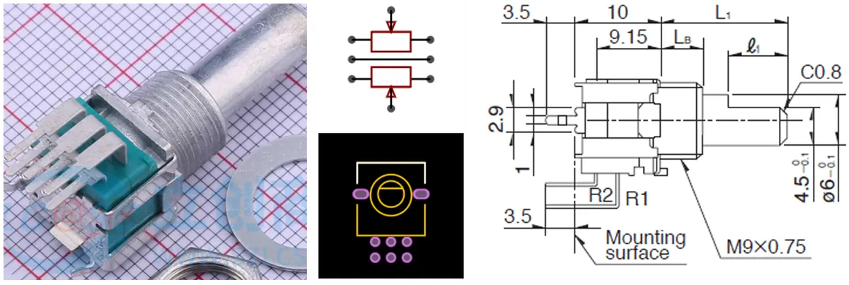
Here, we periodically collect the voltage value from the analog potentiometer, adjust the brightness of the onboard LED based on this voltage value, and meanwhile send the voltage value to SerialPlot, the serial port plotter, to view the voltage waveform.
Here, we need to insert the Fengya No. 1 Board - Universal Compatible Expansion Board into the Fengya No. 1 Board - LCD Screen Human-Machine Interaction Board, and at the same time turn on the Fengya No. 1 Board - LCD Screen Human-Machine Interaction Board 's SWITCH2 DIP switch' s POT option. The physical connection diagram is shown below:
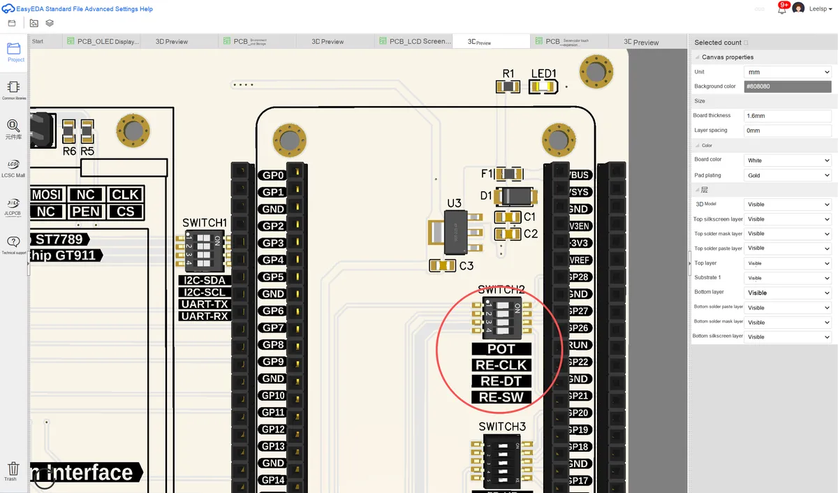
In addition, we also need to connect the MiniUSB data cable to the serial port on the Fengya No. 1 Board - Universal Compatible Expansion Board. Here, GP0 and GP1 are the default pins of the hardware serial port UART0 of the Raspberry Pi Pico:
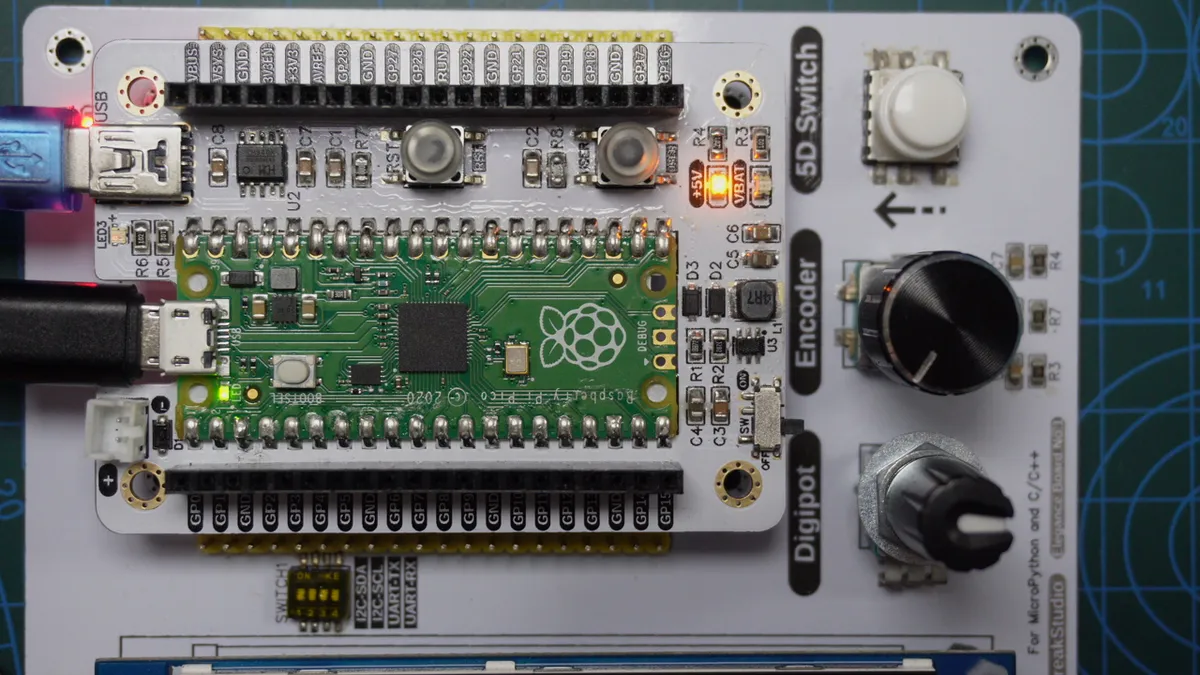
The wiring conditions of the devices are shown in the following table:
Component | Connected Raspberry Pi Pico pins | Notes |
Breathing LED | GP25 | The onboard LED is usually connected to GP25, and this pin is controlled via PWM in the code. |
Analog potentiometer | GP28 (ADC2) | The ADC2 channel is used in the code, which corresponds to GPIO pin GP28 and is used to read the analog signal of the potentiometer. |
USB to TTL Chip (TXD) | GP1 (UART0 RX) | The serial port receiving pin needs to be connected (cross-connected) to the transmitting pin (TXD) of the USB-to-TTL adapter. |
USB to TTL Chip (RXD) | GP0 (UART0 TX) | Serial port transmit pin, which needs to be connected (cross-connected) to the receive pin (RXD) of the USB-to-TTL converter |
USB to TTL Chip (GND) | GND | The GND pin of the Raspberry Pi Pico needs to be connected to the GND of the USB-to-TTL adapter to ensure a common ground; otherwise, the serial communication may malfunction. |
The following code can be found in the elegance-devkit v1\Demo\58 ADC_Potentiometer folder of the resource package we provide.
The sample code is shown below:
# Python env   : MicroPython v1.23.0
# -*- coding: utf-8 -*-
# @Time    : 2024/8/27 11:33 AM
# @Author  : Li Qingshui
# @File    : main.py
# @Description : ADC experiment, read the voltage across the potentiometer

# ======================================== Import Modules ========================================

# Import the hardware module
from machine import ADC, Timer, Pin, PWM, UART
# Import time-related modules
import time
# Import the module for accessing and controlling MicroPython internals
import micropython

# ======================================== Global Variables ============================================

# ======================================== Functions ============================================

# User-defined callback function
def user_callback(value: float) -> None:
    """
    User-defined callback function, used to print the sampled analog potentiometer voltage value.

    Args:
        value (float): The sampled analog potentiometer voltage value.

    Returns:
        None
    """

    # Declare global variables
    global LED, uart

    # Print the sampled analog potentiometer voltage value
    print("Analog potentiometer value is %f" % value)
    # Adjust the LED duty cycle; the duty cycle is ( value / SimulatedPotentiometer.conversion_factor )/ 65535
    LED.duty_u16(int(value/SimulatedPotentiometer.conversion_factor))
    # Send the value over the serial port, formatting the float as a string with two decimal places
    formatted_value = "{:.2f}".format(value)
    uart.write(str(formatted_value)+'\r\n')

# ======================================== Custom Classes ============================================

# Custom simulated potentiometer class
class SimulatedPotentiometer:
    """
    Simulated potentiometer class, used to sample the voltage of an analog potentiometer through an ADC pin and update the data periodically with a timer.

    This class wraps the initialization of the ADC pin and timer, and provides functions to start and stop sampling and to get the current voltage value.
    Supports processing the sampled voltage value through a user-defined callback function.

    Attributes:
        conversion_factor (float): Voltage conversion factor, used to convert the raw ADC value to the actual voltage value.
        adc (ADC): ADC instance, used to read the raw data of the analog potentiometer.
        timer (Timer): Timer instance, used to sample data periodically.
        freq (int): Timer frequency, in Hz.
        value (float): The currently sampled voltage value.
        callback (Optional[Callable[[float], None]]): User-defined callback function, used to process the sampled voltage value.

    Methods:
        __init__(self, adc_id: int, freq: int = 100, callback=None):
            Initialize the simulated potentiometer class instance.
        start(self):
            Start simulated potentiometer sampling.
        _timer_callback(self, timer: Timer):
            Timer callback function, used to sample the voltage value of the simulated potentiometer and convert it.
        stop(self):
            Stop simulated potentiometer sampling.
        get_value(self) -> float:
            Return the current voltage value of the potentiometer.
    """

    # Voltage conversion factor
    conversion_factor = 3.3 / (65535)

    def __init__(self, adc_id: int, freq: int = 100, callback=None) -> None:
        """
        Initialize the simulated potentiometer class.

        Args:
            adc_id (int): The ADC pin number to use; only a number between 0 and 2 can be used.
            freq (int): Timer frequency, 100Hz by default.
            callback (Optional[Callable[[float], None]]): User-defined callback function called after sampling is complete.

        Raises:
            ValueError: If adc_id is not in the range 0~2.
        """

        # Check the entry parameters
        if adc_id > 2 or adc_id < 0:
            raise ValueError("adc_id must be 0~2")

        # Initialize the ADC pin and timer
        self.adc = ADC(adc_id)
        self.timer = Timer(-1)
        self.freq = freq
        # The sampled voltage value
        self.value = 0
        # Reference the user-defined callback function
        self.callback = callback

    def start(self) -> None:
        """
        Start simulated potentiometer sampling.
        Args:
            None

        Returns:
            None
        """
        # Start the timer and set the timer callback function
        self.timer.init(period=int(1000/self.freq), mode=Timer.PERIODIC, callback=self._timer_callback)

    def _timer_callback(self, timer: Timer) -> None:
        """
        Timer callback function, used to sample the voltage value of the simulated potentiometer and convert it.

        Args:
            timer (Timer): Timer object.

        Returns:
            None
        """
        # Read the ADC value and store it in self.value
        self.value = self.adc.read_u16() * SimulatedPotentiometer.conversion_factor
        # Call the user-defined callback function, passing the sampled potentiometer voltage value
        micropython.schedule(self.callback, self.value)

    def stop(self) -> None:
        """
        Stop simulated potentiometer sampling.

        Args:
            None

        Returns:
            None
        """
        # Stop the timer
        self.timer.deinit()

    def get_value(self) -> float:
        """
        Return the current value of the potentiometer.

        Args:
            None

        Returns:
            float: The current voltage value of the potentiometer.
        """
        # Return the current value of the potentiometer
        return self.value

# ======================================== Initialization ==========================================

# Power-on delay
time.sleep(3)
# Print debug information
print("FreakStudio : Analog potentiometer experiment")

# Configure the breathing LED pin
LED = PWM(Pin(25), freq=100, duty_u16=0)

# Create a simulated potentiometer instance, using ADC2-GP28, timer frequency 100Hz, callback function user_callback
potentiometer = SimulatedPotentiometer(2, 100, user_callback)

# Create the serial port object, set the baud rate to 115200
uart = UART(0, 115200)
# Initialize the uart object with a baud rate of 115200, 8 data bits, no parity bit, and 1 stop bit
# Set the serial port timeout to 100ms
uart.init(baudrate  = 115200,
          bits      = 8,
          parity    = None,
          stop      = 1,
          tx        = 0,
          rx        = 1,
          timeout   = 100)

# ========================================  Main Program  ===========================================

# Start the simulated potentiometer
potentiometer.start()
# Run for a while and observe the potentiometer value
time.sleep(20)
# Stop the simulated potentiometer
potentiometer.stop()
# Get the last potentiometer value read
print("Final Potentiometer value:", potentiometer.get_value())
Here, we first define a SimulatedPotentiometer class, which is used to simulate the acquisition operation of a potentiometer: this class reads the voltage of the analog potentiometer through the specified ADC pin, and performs the acquisition operation periodically with the help of a timer.
In the main program, by calling potentiometer.start () to start the acquisition operation of the analog potentiometer, the timer triggers at a frequency of 10 Hz.
When the timer is triggered each time, the _timer_callback function is called. This function reads the current voltage value of the potentiometer and stores it in self.value, then invokes the user-defined callback function user_callback and passes the voltage value to it. user_callback performs the following tasks:
- Adjust the brightness of the LED, which is proportional to the voltage value of the potentiometer
- Format the voltage value into a string with two decimal places, and send it via the serial port
After the simulated potentiometer runs for 20 seconds, stop the timer, obtain the last read potentiometer value, and print it out.
Before flashing the code, we need to complete the configuration of SerialPlot serial plotter:
3.2 Application Experiment.mp4 662 KB
- Configure serial port parameters: On the
Porttab, select the correct serial port (e. g.COM4), set the baud rate to 115200, data bits to 8, stop bits to 1, and no parity bit - Click "Open": After confirming the configuration is correct, click the "
Open" button in the upper right corner to open the serial port

- Select the data format: switch to the
Data Formattab and select the "ASCII" format. In the case of single-channel data transmission, comma is selected as the data separator by default
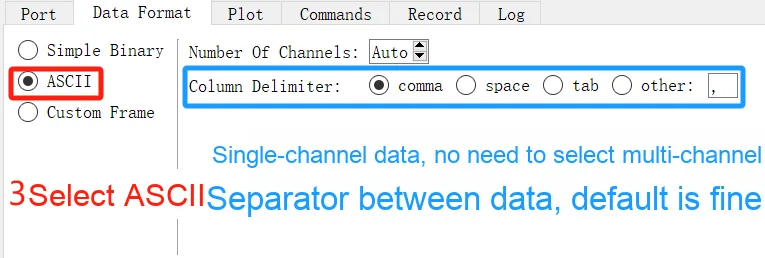
Burning the code, the connection is interrupted, and the output is as follows:
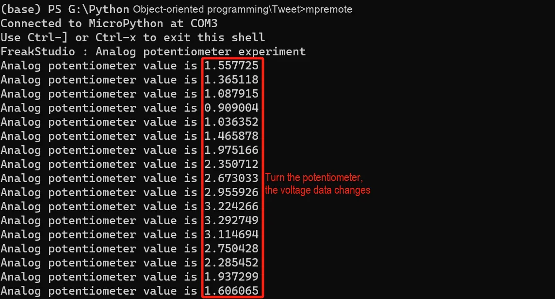
3.2 Application Experiment - Terminal Output.mp4 15.1 MB
It can be seen that as we turn the potentiometer, the voltage data displayed on the terminal keeps changing, and meanwhile the brightness of the onboard LED also varies continuously.
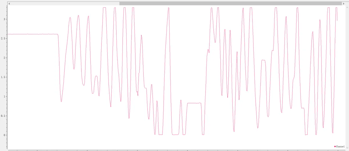
The waveform of the serial port plotter is shown in the figure above, and we can right-click and drag to box-select the waveform we want to examine closely:
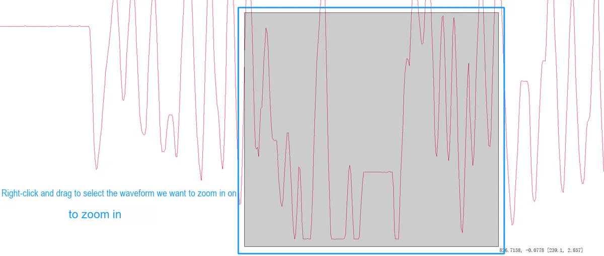
to zoom in for display:
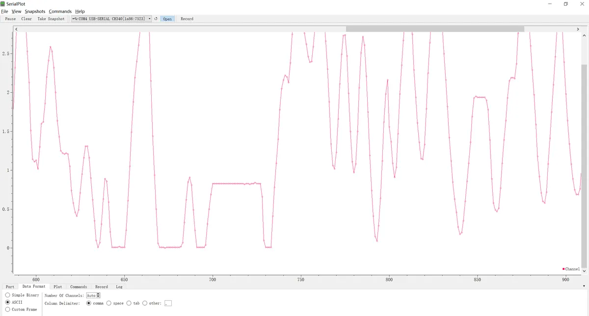
We can also save the received data to a CSV file while it is running:
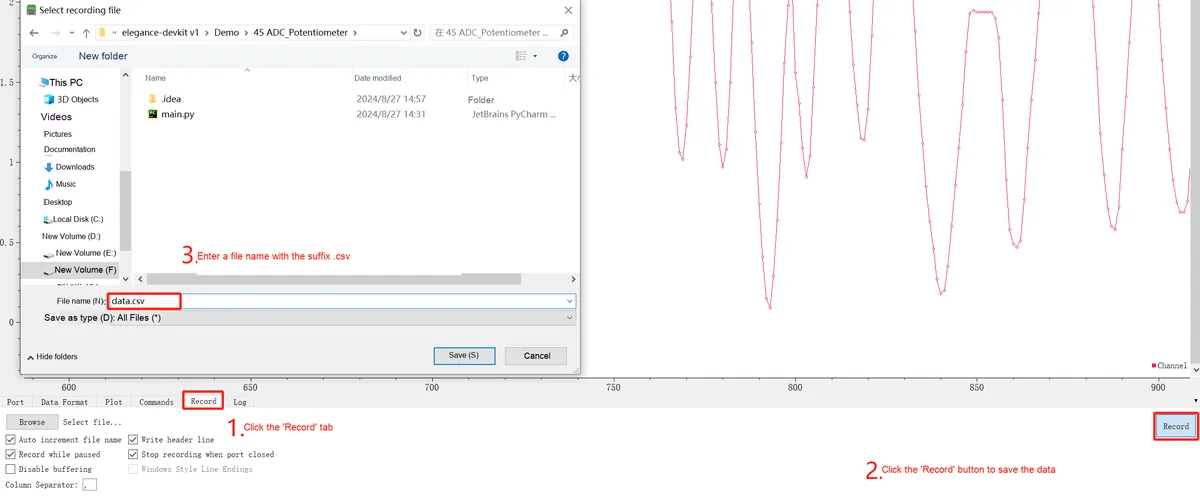
The operation steps are as follows:
- Before receiving data, click the Record tab and the Record button, select a folder to create a new CSV file, or directly enter the desired file name to save, with the file extension being
. csv - Make sure the
Write header lineoption is selected, so that the first line of the file will contain the data headers for easier subsequent analysis. You can also select other options, such as:Auto increment file name: If this option is checked, the system will automatically append a number to the end of the file name to prevent overwriting existing files.Record while paused: Data can still be recorded even when reception is suspendedStop recording when port closed: Automatically stop recording when the serial port is closed
- When you finish receiving the data, click the
Recordbutton to stop recording.
The voltage value data across the potentiometer that was just saved is as follows:
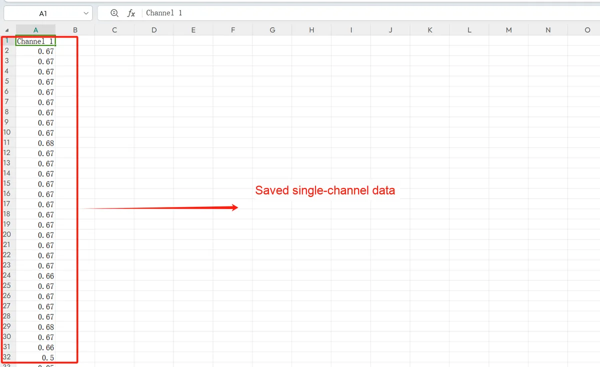
3.2 Application Experiment - PC Software.mp4 10.3 MB
3.3 Joystick Experiment
3.3.1 Basic Principle of the Joystick Module
A joystick module is typically an electronic module that integrates two potentiometers (providing analog voltage signals for the X-axis and Y-axis respectively) and a pushbutton switch. It is widely applied in game controllers, robot control systems and various embedded projects to acquire 2D directional input and the press state of the button.
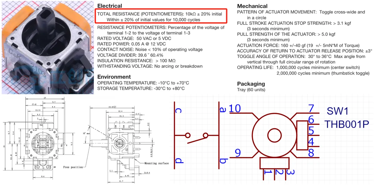
Its basic structure includes:
- X-axis potentiometer (
VRx): Adjusts the output voltage of the potentiometer via horizontal movement of the joystick. As the joystick moves in the horizontal direction, the output voltage of the potentiometer changes accordingly, and this voltage signal is typically read through an ADC (Analog-to-Digital Converter). - Y-axis potentiometer (
VRy): Adjusts the output voltage of the potentiometer via the vertical movement of the joystick. As the joystick moves in the vertical direction, the output voltage of the potentiometer changes accordingly, and this voltage signal is also read through the ADC. - Pushbutton Switch (
VSw): When the joystick is pressed, the internal pushbutton switch is triggered, which normally generates a low-level signal (logic 0); this switch signal can be used to detect whether the joystick is pressed.
The potentiometers on the X-axis and Y-axis generate two independent analog voltage signals via the movement of the joystick, typically ranging from 0V to the reference voltage (e. g., 3.3V); the current position of the joystick can be determined by reading these voltage values.
In our joystick module, a small 1nF capacitor is connected in parallel across both the X-axis potentiometer (VRx) and the Y-axis potentiometer (VRy) to filter out low-frequency noise, and a pull-up resistor is added to the pin of the pushbutton switch (VSw), which outputs a high level when the button is released and a low level when the button is pressed. The schematic diagram is shown below:
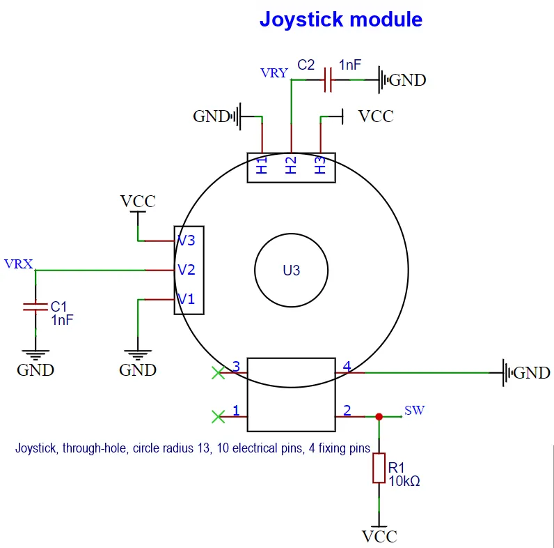
3.3.2 Driver Code Writing
Here, we have customized a Joystick class for reading joystick data, which encapsulates the Data Acquisition logic for the joystick's X-axis, Y-axis and button states. Its main features are as follows:
- Modularization Design: Encapsulate the Data Acquisition logic for the X-axis, Y-axis and button status of the joystick into a class to facilitate reuse and maintenance; implement periodic Data Acquisition via a timer to achieve non-blocking operation.
- Low-pass filtering: The low-pass filtering algorithm is used to smooth the original data collected by the ADC to reduce the impact of noise on the data. Users can adjust the filtering intensity via the
filter_alphaparameter to adapt to different application scenarios. - Callback Mechanism: Supports user-defined callback functions. Once Data Acquisition is completed, the callback function will be automatically invoked to process the data; it uses
micropython.scheduleto ensure that the callback function is executed safely under the scheduling mechanism of MicroPython. - Flexible initialization parameters: support for custom ADC pins, timer frequency and callback function, to adapt to different hardware configurations and application requirements.
- Resource Management: Provides the
startandstopmethods to facilitate the control of the start and stop of Data Acquisition.
The sample code is shown below:
# Custom joystick class
class Joystick:
    """
    Joystick class, used to sample the X-axis and Y-axis voltage values and the button state of a joystick through ADC pins.

    This class wraps the initialization of the ADC pin and timer, and provides functions to start and stop sampling and to get the current voltage value.
    Supports processing the sampled data through a user-defined callback function.

    Attributes:
        conversion_factor (float): Voltage conversion factor, used to convert the raw ADC value to the actual voltage value.
        adc_x (ADC): ADC instance for the X axis.
        adc_y (ADC): ADC instance for the Y axis.
        sw (Pin): Digital input pin instance for the button.
        timer (Timer): Timer instance, used to sample data periodically.
        freq (int): Timer frequency, in Hz.
        x_value (float): The currently sampled X-axis voltage value.
        y_value (float): The currently sampled Y-axis voltage value.
        sw_value (int): The currently sampled button state (0 or 1).
        callback (Optional[Callable[[tuple], None]]): User-defined callback function, used to process the sampled data.
        filter_alpha (float): Low-pass filter coefficient.
        filtered_x (float): Filtered X-axis voltage value.
        filtered_y (float): Filtered Y-axis voltage value.

    Methods:
        __init__(self, vrx_pin: int, vry_pin: int, vsw_pin: int, freq: int = 100, callback=None):
            Initialize the joystick class instance.
        start(self):
            Start joystick data sampling.
        _timer_callback(self, timer: Timer):
            Timer callback function, used to sample the X-axis, Y-axis and button state of the joystick.
        stop(self):
            Stop data sampling.
        get_values(self) -> tuple:
            Get the current X-axis, Y-axis and button state of the joystick.
    """

    # Voltage conversion factor
    conversion_factor = 3.3 / (65535)

    def __init__(self, vrx_pin: int, vry_pin: int, vsw_pin: int, freq: int = 100, callback: callable[[tuple], None] = None) -> None:
        """
        Initialize the joystick class.

        Args:
            vrx_pin (int): ADC pin number for the X axis.
            vry_pin (int): ADC pin number for the Y axis.
            vsw_pin (int): Digital input pin number for the button.
            freq (int): Timer frequency, 100Hz by default.
            callback (Optional[Callable[[tuple], None]]): User-defined callback function after data sampling.

        Returns:
            None
        """
        # Initialize the ADC pins
        self.adc_x = ADC(vrx_pin)
        self.adc_y = ADC(vry_pin)
        # Initialize the button pin
        self.sw = Pin(vsw_pin, Pin.IN, Pin.PULL_UP)

        # Initialize the timer
        self.timer = Timer(-1)
        self.freq = freq

        # Save the collected values
        self.x_value = 0
        self.y_value = 0
        self.sw_value = 1

        # Reference the user-defined callback function
        self.callback = callback

        # Initialize filter parameters
        # Low-pass filter coefficient
        self.filter_alpha = 0.2
        # Initial value is the midpoint
        self.filtered_x = 1.55
        # Initial value is the midpoint
        self.filtered_y = 1.55

    def start(self) -> None:
        """
        Start joystick data sampling.

        Args:
            None

        Returns:
            None
        """
        self.timer.init(period=int(1000/self.freq), mode=Timer.PERIODIC, callback=self._timer_callback)

    def _timer_callback(self, timer: Timer) -> None:
        """
        Timer callback function, used to sample the X-axis, Y-axis and button state of the joystick.

        Args:
            timer (Timer): Timer object.

        Returns:
            None
        """
        # Read the ADC values of the X axis and Y axis
        raw_x = self.adc_x.read_u16() * Joystick.conversion_factor
        raw_y = self.adc_y.read_u16() * Joystick.conversion_factor
        # Low-pass filter
        self.filtered_x = self.filter_alpha * raw_x + (1 - self.filter_alpha) * self.filtered_x
        self.filtered_y = self.filter_alpha * raw_y + (1 - self.filter_alpha) * self.filtered_y
        # Update values
        self.x_value = self.filtered_x
        self.y_value = self.filtered_y

        # Read the button state: 0 when pressed, 1 when not pressed
        self.sw_value = self.sw.value()

        # Call the user-defined callback function, passing the collected X-axis and Y-axis voltage values and the button state
        micropython.schedule(self.callback, (self.x_value, self.y_value, self.sw_value))

    def stop(self) -> None:
        """
        Stop data sampling.

        Args:
            None

        Returns:
            None
        """
        self.timer.deinit()

    def get_values(self) -> tuple:
        """
        Get the current X-axis, Y-axis and button state of the joystick.

        Args:
            None

        Returns:
            tuple: A tuple containing the X-axis and Y-axis voltage values and the button state, in the format (x_value, y_value, sw_value).
        """
        return self.x_value, self.y_value, self.sw_value
The following methods are included:
__init__()method: Initializes the joystick object, including the ADC pin, button pin and timer.The callbackparameter is used to specify the callback function after Data Acquisition, and here we fix the low-pass filtering coefficient to 0.2.start ()Method: Starts a timer to periodically read joystick data; the timer runs at the specified interval of1000 / freqmilliseconds._timer_callback ()Method: A timer callback function, which is used to read the X-axis, Y-axis and button status of the joystick, call the user-defined callback function, and perform low-pass filtering on the ADC value to reduce the impact of noise; here,micropython.scheduleis used to call the user-defined callback function to ensure that the callback function is executed in the main thread.stop ()Method: Stop Data Acquisition, release hardware resources, that is, use theTimer.deinitmethod to stop the timer.get_values ()method: Obtains the X-axis, Y-axis and button status of the current joystick, and returns a tuple(x_value, y_value, sw_value).
3.3.3 Preparations before the Experiment
In the following experiment, we need to insert the Fengya No. 1 Board - Universal Compatible Expansion Board into the Fengya No. 1 Board - OLED Display and Interaction Expansion Board, and at the same time turn on the Fengya No. 1 Board - OLED Display and Interaction Expansion Board 's SWITCH1 DIP switch' s I2C_SDA and I2C_SCL options:
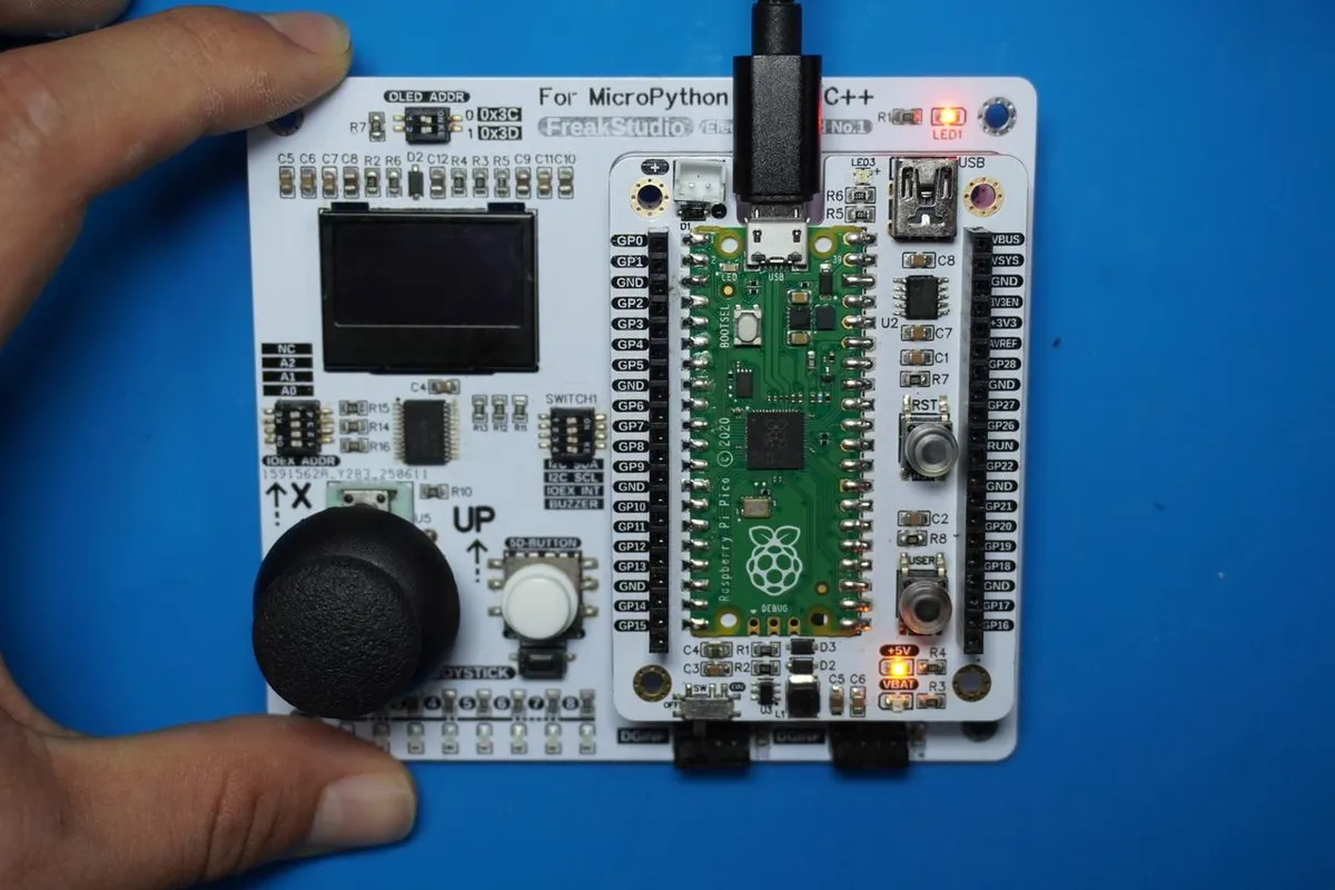
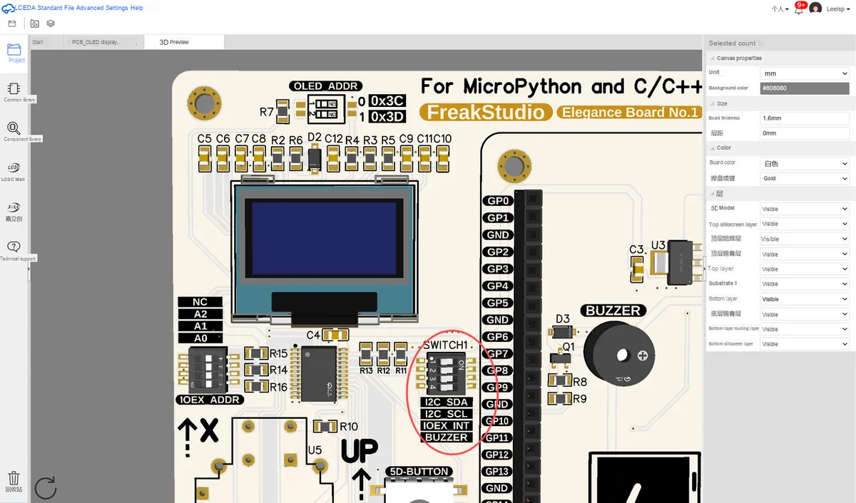
In addition, please select an address on the OLED_ADDR DIP switch. This example sets the switch to 0x3C, so the OLED screen's I²C address is 0x3C:
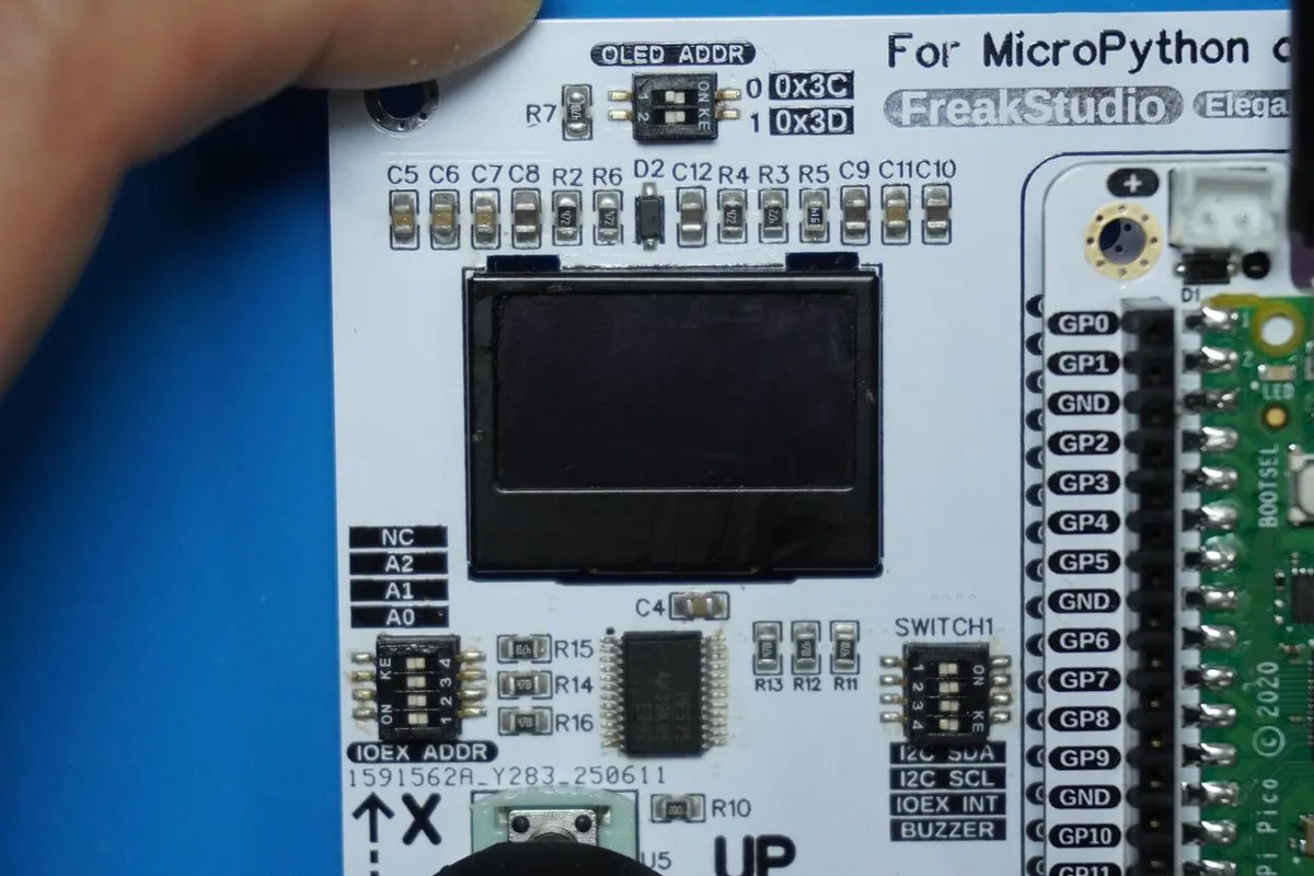
The wiring of the components is shown in the following table:
Component | Connected Raspberry Pi Pico pins | Notes |
OLED Screen (SDA) | GP6 | I2C data pin, connected to the SDA pin of the OLED screen |
OLED Screen (SCL) | GP7 | I2C clock pin, connected to the SCL pin of the OLED screen |
OLED Screen (VCC) | 3.3V | Screen power supply (specified in the code that no external power supply is used, which is normally 3.3V provided by the Pico) |
OLED Display (GND) | GND | Grounding, must share a common ground with Pico |
Joystick X-axis (VRX) | GP26 (ADC0) | Analog output of the joystick X-axis, connected to the ADC0 channel (corresponding to GP26) of the Pico |
Joystick Y-axis (VRY) | GP27 (ADC1) | Analog output of the joystick Y-axis, connected to the ADC1 channel of the Pico (corresponding to GP27) |
Joystick Switch (VSW) | GP22 | The built-in button pin of the joystick is connected to GP22 of the Pico, and it will be grounded when the button is pressed. |
Joystick (VCC) | 3.3V | Joystick power supply, connect to 3.3V |
Joystick (GND) | GND | Grounding, must share a common ground with Pico |
3.3.4 Application Experiment
The following code can be found in the folder elegance-devkit v1\Demo\59 ADC_Joystick included in the resource package we provide.
In the following code, we have designed a joystick-controlled game, which controls the movement of a ball on the OLED screen by reading the voltage value of the joystick. The sample code is shown below:
# Python env   : MicroPython v1.23.0
# -*- coding: utf-8 -*-
# @Time    : 2024/8/27 10:02 PM
# @Author  : Li Qingshui
# @File    : main.py
# @Description : ADC experiment, read the voltages at both ends of the joystick

# ======================================== Import Modules ========================================

# Import the hardware module
from machine import ADC, Timer, Pin, I2C
# Import time-related modules
import time
# Import the module for accessing and controlling MicroPython internals
import micropython
# Import the ssd1306 display modules
from ssd1306 import SSD1306_I2C

# ======================================== Global Variables ============================================

# OLED screen address
OLED_ADDRESS = 0

# ======================================== Functions ============================================

def user_callback(data: tuple) -> None:
    """
    User-defined callback function for processing the collected joystick data.

    Args:
        data (tuple): A tuple containing the joystick's X-axis and Y-axis voltage values and the button state, in the format (x_value, y_value, sw_value).

    Returns:
        None
    """
    # Declare global variables
    global ball

    # Print the joystick data values
    x_value, y_value, sw_value = data
    print("X: {:.2f}, Y: {:.2f}, Switch: {}".format(x_value, y_value, sw_value))

    # Move the ball
    ball.move_ball(x_value,y_value)

# ======================================== Custom Classes ============================================

# Custom joystick class
class Joystick:
    """
    Joystick class, used to sample the X-axis and Y-axis voltage values and the button state of a joystick through ADC pins.

    This class wraps the initialization of the ADC pin and timer, and provides functions to start and stop sampling and to get the current voltage value.
    Supports processing the sampled data through a user-defined callback function.

    Attributes:
        conversion_factor (float): Voltage conversion factor, used to convert the raw ADC value to the actual voltage value.
        adc_x (ADC): ADC instance for the X axis.
        adc_y (ADC): ADC instance for the Y axis.
        sw (Pin): Digital input pin instance for the button.
        timer (Timer): Timer instance, used to sample data periodically.
        freq (int): Timer frequency, in Hz.
        x_value (float): The currently sampled X-axis voltage value.
        y_value (float): The currently sampled Y-axis voltage value.
        sw_value (int): The currently sampled button state (0 or 1).
        callback (Optional[Callable[[tuple], None]]): User-defined callback function, used to process the sampled data.
        filter_alpha (float): Low-pass filter coefficient.
        filtered_x (float): Filtered X-axis voltage value.
        filtered_y (float): Filtered Y-axis voltage value.

    Methods:
        __init__(self, vrx_pin: int, vry_pin: int, vsw_pin: int, freq: int = 100, callback=None):
            Initialize the joystick class instance.
        start(self):
            Start joystick data sampling.
        _timer_callback(self, timer: Timer):
            Timer callback function, used to sample the X-axis, Y-axis and button state of the joystick.
        stop(self):
            Stop data sampling.
        get_values(self) -> tuple:
            Get the current X-axis, Y-axis and button state of the joystick.
    """

    # Voltage conversion factor
    conversion_factor = 3.3 / (65535)

    def __init__(self, vrx_pin: int, vry_pin: int, vsw_pin: int, freq: int = 100, callback: callable[[tuple], None] = None) -> None:
        """
        Initialize the joystick class.

        Args:
            vrx_pin (int): ADC pin number for the X axis.
            vry_pin (int): ADC pin number for the Y axis.
            vsw_pin (int): Digital input pin number for the button.
            freq (int): Timer frequency, 100Hz by default.
            callback (Optional[Callable[[tuple], None]]): User-defined callback function after data sampling.

        Returns:
            None
        """
        # Initialize the ADC pins
        self.adc_x = ADC(vrx_pin)
        self.adc_y = ADC(vry_pin)
        # Initialize the button pin
        self.sw = Pin(vsw_pin, Pin.IN, Pin.PULL_UP)

        # Initialize the timer
        self.timer = Timer(-1)
        self.freq = freq

        # Save the collected values
        self.x_value = 0
        self.y_value = 0
        self.sw_value = 1

        # Reference the user-defined callback function
        self.callback = callback

        # Initialize filter parameters
        # Low-pass filter coefficient
        self.filter_alpha = 0.2
        # Initial value is the midpoint
        self.filtered_x = 1.55
        # Initial value is the midpoint
        self.filtered_y = 1.55

    def start(self) -> None:
        """
        Start joystick data sampling.

        Args:
            None

        Returns:
            None
        """
        self.timer.init(period=int(1000/self.freq), mode=Timer.PERIODIC, callback=self._timer_callback)

    def _timer_callback(self, timer: Timer) -> None:
        """
        Timer callback function, used to sample the X-axis, Y-axis and button state of the joystick.

        Args:
            timer (Timer): Timer object.

        Returns:
            None
        """
        # Read the ADC values of the X axis and Y axis
        raw_x = self.adc_x.read_u16() * Joystick.conversion_factor
        raw_y = self.adc_y.read_u16() * Joystick.conversion_factor
        # Low-pass filter
        self.filtered_x = self.filter_alpha * raw_x + (1 - self.filter_alpha) * self.filtered_x
        self.filtered_y = self.filter_alpha * raw_y + (1 - self.filter_alpha) * self.filtered_y
        # Update values
        self.x_value = self.filtered_x
        self.y_value = self.filtered_y

        # Read the button state: 0 when pressed, 1 when not pressed
        self.sw_value = self.sw.value()

        # Call the user-defined callback function, passing the collected X-axis and Y-axis voltage values and the button state
        micropython.schedule(self.callback, (self.x_value, self.y_value, self.sw_value))

    def stop(self) -> None:
        """
        Stop data sampling.

        Args:
            None

        Returns:
            None
        """
        self.timer.deinit()

    def get_values(self) -> tuple:
        """
        Get the current X-axis, Y-axis and button state of the joystick.

        Args:
            None

        Returns:
            tuple: A tuple containing the X-axis and Y-axis voltage values and the button state, in the format (x_value, y_value, sw_value).
        """
        return self.x_value, self.y_value, self.sw_value

# Ball game class: control the ball's movement through input coordinates
class Ballgame:
    """
    Ball game class, used to control the movement of a ball on the OLED display through joystick input.

    This class encapsulates the ball's initialization, drawing and movement logic. It supports controlling the ball's movement through joystick input and detects whether the ball hits the rectangular border.

    Attributes:
        ball_x (int): X-axis coordinate of the ball.
        ball_y (int): Y-axis coordinate of the ball.
        ball_size (int): Size of the ball.
        rect_w (int): Width of the rectangular border.
        rect_h (int): Height of the rectangular border.
        rect_x (int): X-axis coordinate of the rectangular border.
        rect_y (int): Y-axis coordinate of the rectangular border.
        oled (SSD1306_I2C): OLED display instance.

    Methods:
        __init__(self, oled_obj: SSD1306_I2C, rect_x: int, rect_y: int, rect_w: int, rect_h: int):
            Initialize the ball game class.
        draw_ball(self):
            Draw the ball.
        move_ball(self, x: float, y: float):
            Move the ball according to joystick input.
    """
    def __init__(self, oled_obj: SSD1306_I2C, rect_x: int, rect_y: int, rect_w: int, rect_h: int) -> None:
        """
        Initialize the ball game class.

        Args:
            oled_obj (SSD1306_I2C): The OLED display instance to use.
            rect_x (int): X-axis coordinate of the rectangular border.
            rect_y (int): Y-axis coordinate of the rectangular border.
            rect_w (int): Width of the rectangular border.
            rect_h (int): Height of the rectangular border.

        Returns:
            None
        """

        # Set the ball's initial parameters: coordinates and size
        self.ball_x = rect_x + int(rect_w/2)
        self.ball_y = rect_y + int(rect_h/2)
        self.ball_size = 5

        # Set the rectangular border parameters
        self.rect_w = rect_w
        self.rect_h = rect_h
        self.rect_x = rect_x
        self.rect_y = rect_y

        # Set the OLED display object to use
        self.oled = oled_obj

        # Draw the rectangular border
        self.oled.rect(self.rect_x, self.rect_y, self.rect_w, self.rect_h, 1)
        # Draw the ball
        self.draw_ball()
        # Display an image
        self.oled.show()

    def draw_ball(self) -> None:
        """
        Draw the ball.

        Args:
            None

        Returns:
            None
        """
        self.oled.fill_rect(int(self.ball_x - self.ball_size), int(self.ball_y - self.ball_size),
                            self.ball_size * 2, self.ball_size * 2, 1)

    def move_ball(self, x: float, y: float) -> None:
        """
        Move the ball.

        Args:
            x (float): Voltage value of the joystick X axis.
            y (float): Voltage value of the joystick Y axis.

        Returns:
            None
        """

        # Calibrate the joystick input so that the midpoint is close to 0
        x -= 1.55  # The offset is the midpoint, 1.65V
        y -= 1.55  # The offset is the midpoint, 1.65V

        # # Invert the Y-axis value
        # y = -y

        # Add a dead zone: when the ADC value is within the dead zone, the joystick is treated as not operated and the ball does not move
        dead_zone = 0.2
        if abs(x) < dead_zone:
            x = 0
        if abs(y) < dead_zone:
            y = 0

        # Limit the joystick value range
        x = max(min(x, 1.55), -1.55)
        y = max(min(y, 1.55), -1.55)

        # Map the voltage value to the ball speed range (for example, -4 to 4 pixels/frame)
        speed_x = (x / 1.55) * 4  # Speed range is from -4 to 4
        speed_y = (y / 1.55) * 4  # Speed range is from -4 to 4

        # Move the ball according to the joystick value
        self.ball_x += speed_x
        self.ball_y += speed_y

        # Detect whether the ball hits the rectangular border, and bounce it back if so
        if self.ball_x - self.ball_size < self.rect_x or self.ball_x + self.ball_size > self.rect_x + self.rect_w:
            self.ball_x = max(self.rect_x + self.ball_size,
                              min(self.ball_x, self.rect_x + self.rect_w - self.ball_size))
        if self.ball_y - self.ball_size < self.rect_y or self.ball_y + self.ball_size > self.rect_y + self.rect_h:
            self.ball_y = max(self.rect_y + self.ball_size,
                              min(self.ball_y, self.rect_y + self.rect_h - self.ball_size))

        # Clear the screen and redraw the rectangular border and the ball
        self.oled.fill_rect(self.rect_x, self.rect_y, self.rect_w, self.rect_h, 0)
        self.oled.rect(self.rect_x, self.rect_y, self.rect_w, self.rect_h, 1)
        self.draw_ball()
        # Display the ball
        self.oled.show()

# ======================================== Initialization ==========================================

# Delay 3 s to wait for the device to finish powering up
time.sleep(3)
# Print debug information
print("FreakStudio : reading the voltage value of Joystick experiment")

# Create a hardware I2C instance using the I2C1 peripheral, clock frequency 400KHz, SDA pin 6, SCL pin 7
i2c = I2C(id=1, sda=Pin(6), scl=Pin(7), freq=400000)

# Start scanning for devices on the I2C bus and return a list of slave addresses
devices_list = i2c.scan()
print('START I2C SCANNER')

# If devices_list is empty, no device is connected to the I2C bus
if len(devices_list) == 0:
    print("No i2c device !")
# If not empty, print the slave device addresses
else:
    print('i2c devices found:', len(devices_list))
    # Iterate over the slave device address list
    for device in devices_list:
        # Check whether the slave device address is 0x3c or 0x3d (i.e., the address of the OLED SSD1306)
        if device == 0x3c or device == 0x3d:
            print("I2C hexadecimal address: ", hex(device))
            OLED_ADDRESS = device

# Create an SSD1306 OLED screen instance, width 128 pixels, height 64 pixels, without external power supply
oled = SSD1306_I2C(i2c, OLED_ADDRESS, 128, 64,False)
# Print a prompt message
print('OLED init success')

# The (0,0) origin is at the top-left corner of the screen, with the positive x-axis to the right and the positive y-axis downward
# Display text
oled.text('Freak Studio', 0, 5)
oled.text('Joystick Test', 0, 15)
# Display an image
oled.show()

# Create the joystick instance, using ADC0-GP26 and ADC1-GP27 as the Y axis and X axis, and GP22 as the button
joystick = Joystick(vrx_pin=0, vry_pin=1, vsw_pin=22, freq=10, callback=user_callback)

# Create the ball game class
ball = Ballgame(oled, 5,25,120,35)

# ========================================  Main Program  ===========================================

# Start joystick data collection
joystick.start()
# Run for a while and observe the joystick state
time.sleep(30)
# Stop data collection
joystick.stop()
# Get the last joystick values read
x_val, y_val, sw_val = joystick.get_values()
print("Final Joystick values: X = {:.2f}, Y = {:.2f}, Switch = {}".format(x_val, y_val, sw_val))
Here, in addition to the Joystick joystick class, we also define a Ballgame ball game class, which is a utility class for implementing a ball movement game on an OLED screen. Its basic working principle is to calculate the moving speed and direction of the ball according to the voltage value input by the joystick, and then update the position of the ball. It defines three methods: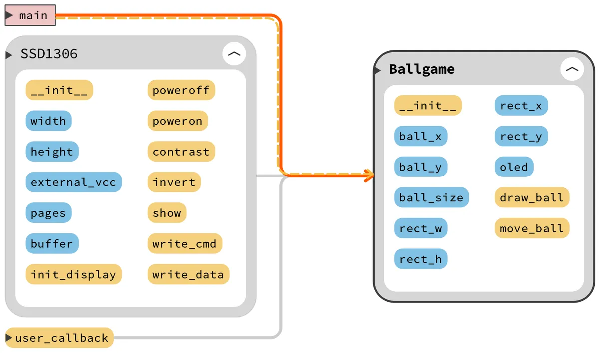
__init__()Initialization Method: Initialize the ball game class, set the initial position of the ball to the center of the rectangular border, and configure the rectangular border parameters and the OLED screen object at the same time.draw_ball ()Draw ball method: Use thefill_rect ()method to draw a solid rectangle to represent the ball. The position of the ball is determined byball_xandball_y, and its size is determined byball_size.move_ball ()Ball movement method: The basic function is to move the ball according to the joystick input and detect whether it touches the rectangular border, which includes the following steps: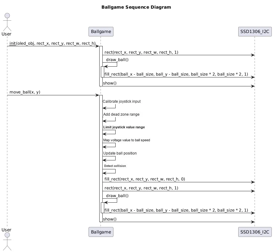
- Calibrate joystick input: Subtract the intermediate value (1.55V) from the voltage value of the joystick input to bring the intermediate value close to 0, and invert the Y-axis value at the same time to ensure that the joystick input is consistent with the direction of the screen coordinates.
- Dead zone processing: When the joystick input falls within the dead zone range, the joystick is regarded as being unoperated and the ball will not move, so as to prevent the position drift of the ball caused by ADC noise.
- Restrict Joystick Value Range and Coordinate Mapping: Limit the joystick input to the valid range (-1.55V to 1.55V), and meanwhile map the voltage value of the joystick input to the velocity range of the ball. Here, the voltage value range of the joystick input is -1.55V to 1.55V, corresponding to the ball's velocity range of -4 to 4 pixels per frame.
- Update the position of the ball: Update the X-axis and Y-axis coordinates of the ball according to the calculated velocity, and detect whether the ball hits the rectangular border; if it does, make the ball bounce. Meanwhile, continuously clear the screen and redraw the rectangular frame and the ball to achieve a dynamic display effect.
All the above procedures perform the following tasks:
- Create an I2C instance, scan the devices on the bus, and identify the address of the OLED screen
- Create an OLED screen object and display the initial text
- Create a joystick object, set the ADC pins for the X-axis and Y-axis as well as the button pin, and specify the callback function
- Create a ball game object, and initialize the rectangular border and the ball.
The overall process is shown in the following figure:
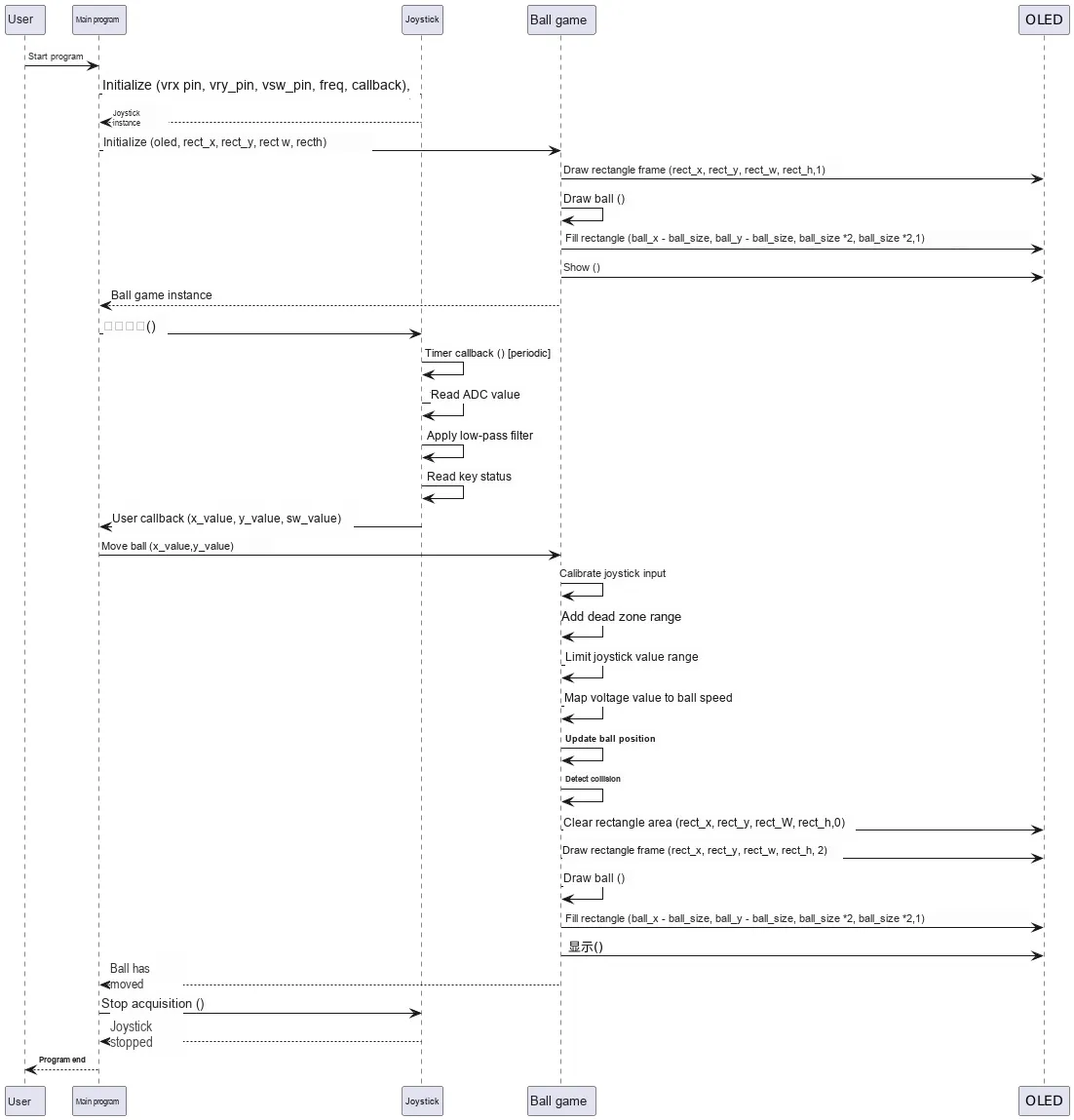
In the main program, we start the joystick Data Acquisition, collect joystick data periodically and in the user-defined callback function user_callback, print the voltage values of the two potentiometers of the joystick, and adjust the position of the ball according to the voltage values.
Burn the code, open the terminal, and the following content will be displayed:
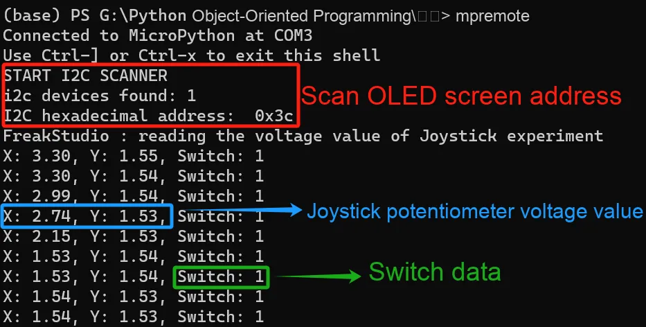
It can be seen that the potentiometer data and switch data of the joystick are printed normally, and as the joystick moves, OLED the small ball inside the rectangle on the screen also moves accordingly:
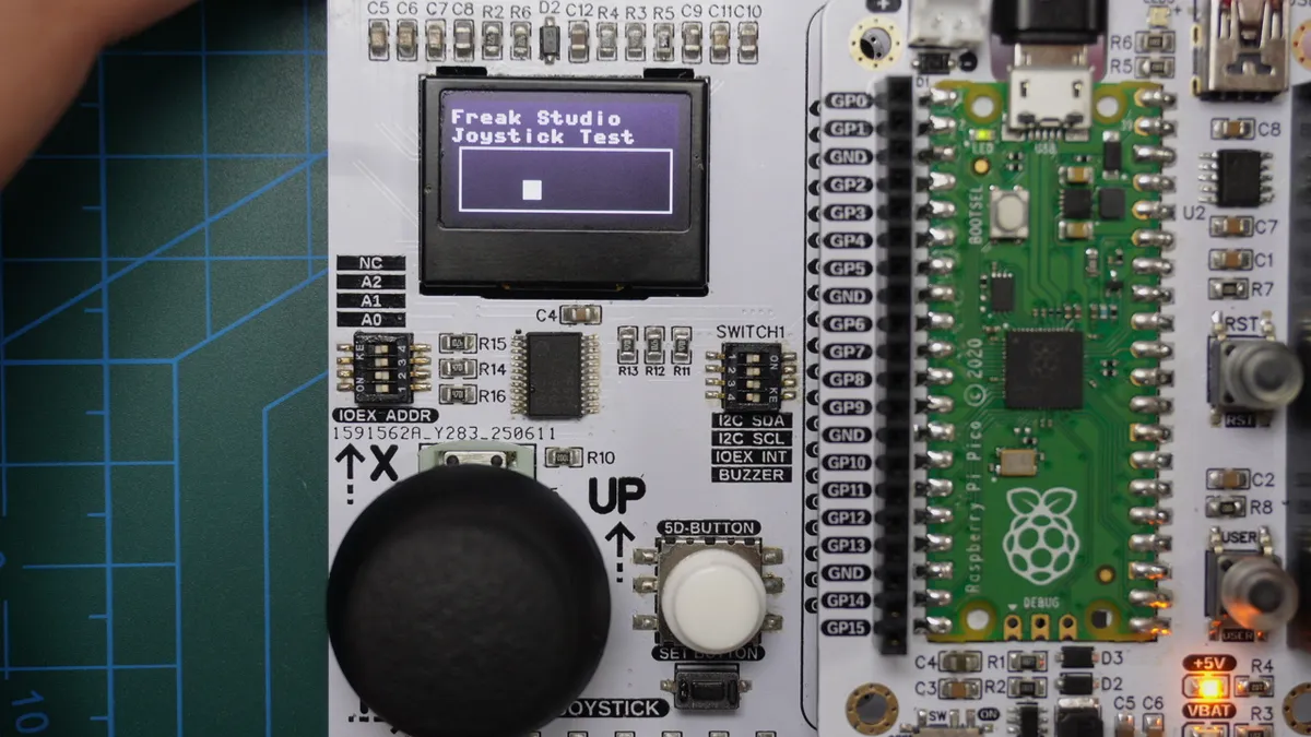
3.3 Application Experiment.mp4 49.1 MB
3.4 Reading the External ADC Chip ADS1115 via I2C
3.4.1 Preparations Before the Experiment
In the following experiment, we need to insert the Fengya No. 1 Board - Data Conversion Board into the Fengya No. 1 Board - Universal Compatible Expansion Board, and meanwhile turn on the SCL, SDA and RDY options of the SWITCH1 DIP switch on the Fengya No. 1 Board - Data Conversion Board:
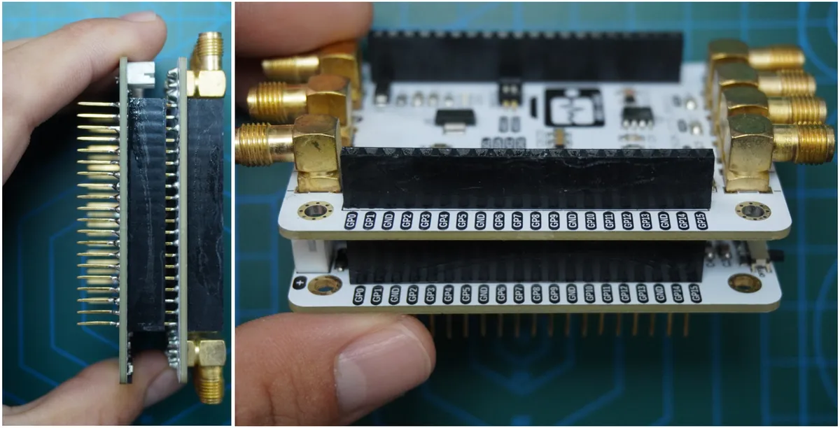
In addition, please select an address on the ADS1115 chip address selection ADDR dip switch (only one option can be toggled). In this example, the GND of the dip switch is turned on, so the ADS1115 chip's I²C address is 0x48:
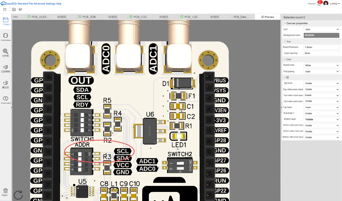
In the Fengya No. 1 board - data conversion board, in terms of the hardware design of the ADC module, we add a 1nF small filtering capacitor to each AIN input channel to filter out high-frequency noise, and meanwhile add a power supply π-type LC filtering circuit in the power supply section to ensure stable power supply:
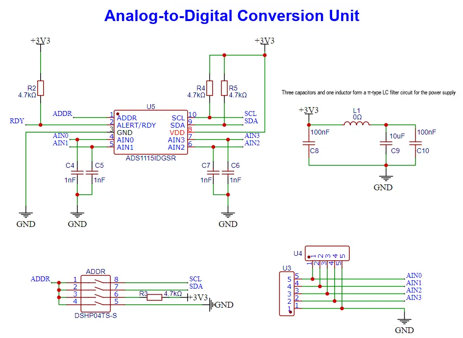
In addition, we first need to connect the MiniUSB data cable to the serial port on Fengya No. 1 Board - Universal Compatible Expansion Board. Here, GP0 and GP1 are the default pins of the hardware serial port UART0 of the Raspberry Pi Pico:
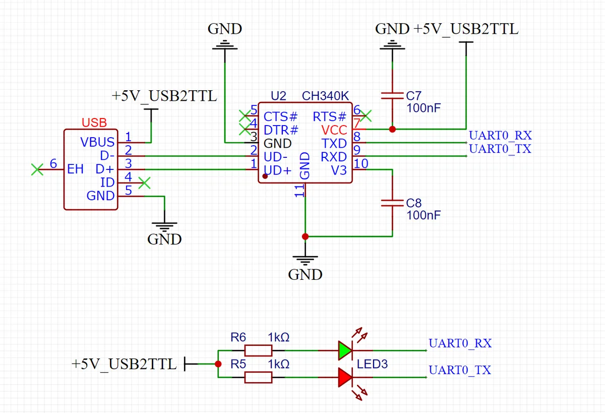
The physical image after insertion is as follows:
The wiring conditions are shown in the following table:
Component | Connected Raspberry Pi Pico pins | Notes |
USB to TTL Chip (TXD) | GP1 (UART0 RX) | Serial port receive pin, cross-connected to the transmit pin (TXD) of the USB-to-TTL converter |
USB to TTL Chip (RXD) | GP0 (UART0 TX) | The serial port transmission pin is cross-connected with the receiving pin (RXD) of the USB-to-TTL converter. |
USB to TTL Chip (GND) | GND | Connect to a common ground to ensure consistent level reference for serial communication |
ADS1115 (SDA) | GP2 | I2C data pin, connected to the SDA pin of the ADS1115 |
ADS1115 (SCL) | GP3 | I2C clock pin, connected to the SCL pin of the ADS1115 |
ADS1115 (VCC) | 3.3V | Power supply pin, to be selected according to the specifications of the ADS1115 module |
ADS1115 (GND) | GND | Connect to a common ground and link it to the GND of the Pico to ensure stable I2C communication. |
Here, on the Fengya No. 1 board - data conversion board, the signal input interface used by the ADC analog-to-digital conversion unit is an SMA interface. We also need to use an SMA to MCX adapter cable to connect the ADC analog-to-digital conversion unit's AIN0 input to the signal output interface DDS of the handheld signal generator:
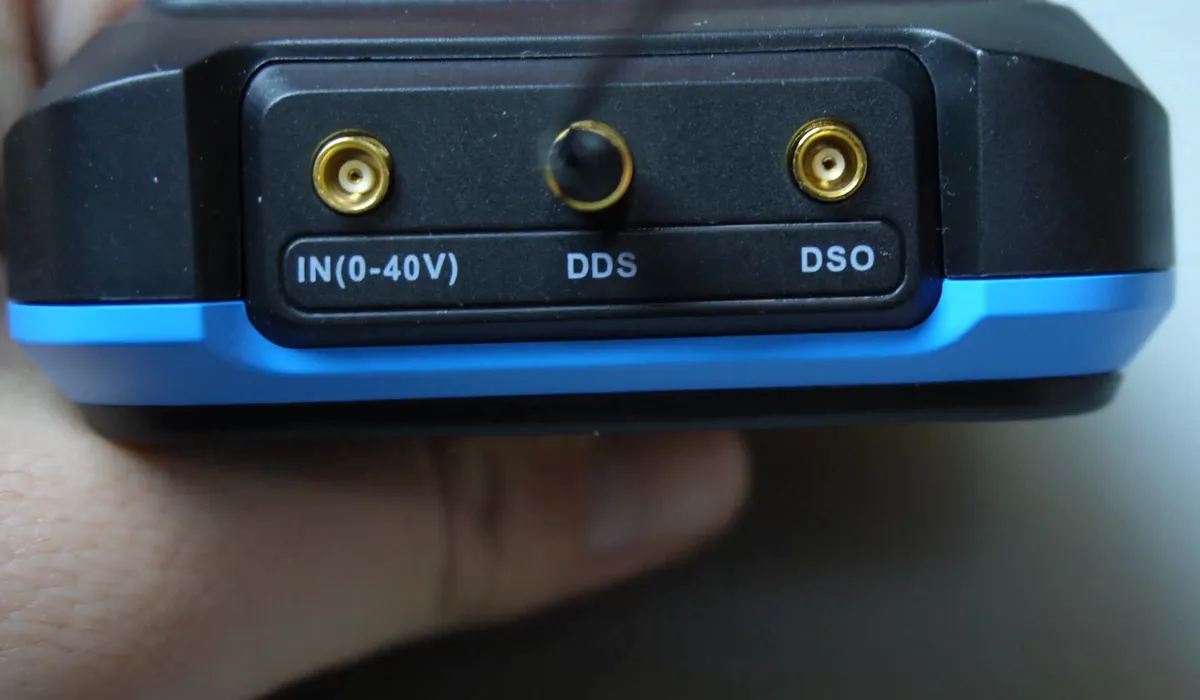
The complete physical connection diagram is shown as follows:
3.4.2 Implementation of Custom ADS1115 Class
In the following code, we have customized a ADS1115 chip communication and control class named ADS1115, which interacts with the ADS1115 chip via the I2C interface and provides functions such as configuration, data reading, and interrupt handling.
The sample code is shown below:
# Python env   : MicroPython v1.23.0
# -*- coding: utf-8 -*-
# @Time    : 2024/10/7 2:24 PM
# @Author  : Li Qingshui
# @File    : ads1115.py
# @Description : Driver class for the external ADC chip ADS1115
# Reference code: https://github.com/robert-hh/ads1x15
# This part of the code was developed by robert-hh and released under the MIT license.

# ======================================== Import Modules =========================================

# Import time-related modules
import time
# Import MicroPython-related modules
from micropython import const
import micropython
# Import hardware-related modules
from machine import Pin, I2C

# ======================================== Global Variables ============================================

# ======================================== Functions ============================================

# ======================================== Custom Classes ============================================

# Custom ADS1115 class
class ADS1115:
    """
    The ADS1115 class is used to control the ADS1115 external ADC chip. It exchanges data with the sensor through the I2C interface, reads analog signals and converts them to digital signals.

    Attributes:
        i2c (machine.I2C): I2C interface object used to communicate with the ADS1115.
        address (int): I2C address of the ADS1115, 0x48 by default.
        gain_index (int): Index of the current gain setting.
        alert_pin (Pin, optional): Alert pin, which provides external interrupt notification. Defaults to None.
        callback (Callable, optional): Callback function called when the alert triggers. Defaults to None.

    Class Variables:
        REGISTER_CONVERT (const): Address of the conversion register.
        REGISTER_CONFIG (const): Address of the configuration register.
        REGISTER_LOWTHRESH (const): Address of the low threshold register.
        REGISTER_HITHRESH (const): Address of the high threshold register.
        OS_MASK (const): Operational status mask.
        OS_SINGLE (const): Start a single conversion.
        OS_BUSY (const): Conversion in progress when read.
        OS_NOTBUSY (const): Conversion complete when read.
        MUX_MASK (const): Multiplexer mask.
        MUX_DIFF_0_1 (const): Differential input: AIN0 - AIN1.
        MUX_DIFF_0_3 (const): Differential input: AIN0 - AIN3.
        MUX_DIFF_1_3 (const): Differential input: AIN1 - AIN3.
        MUX_DIFF_2_3 (const): Differential input: AIN2 - AIN3.
        MUX_SINGLE_0 (const): Single-ended input: AIN0.
        MUX_SINGLE_1 (const): Single-ended input: AIN1.
        MUX_SINGLE_2 (const): Single-ended input: AIN2.
        MUX_SINGLE_3 (const): Single-ended input: AIN3.
        PGA_MASK (const): Programmable gain mask.
        PGA_6_144V (const): +/-6.144V range, gain 2/3.
        PGA_4_096V (const): +/-4.096V range, gain 1.
        PGA_2_048V (const): +/-2.048V range, gain 2.
        PGA_1_024V (const): +/-1.024V range, gain 4.
        PGA_0_512V (const): +/-0.512V range, gain 8.
        PGA_0_256V (const): +/-0.256V range, gain 16.
        MODE_MASK (const): Mode mask.
        MODE_CONTIN (const): Continuous conversion mode.
        MODE_SINGLE (const): Single conversion mode.
        DR_MASK (const): Data rate mask.
        DR_8SPS (const): 8 samples per second.
        DR_16SPS (const): 16 samples per second.
        DR_32SPS (const): 32 samples per second.
        DR_64SPS (const): 64 samples per second.
        DR_128SPS (const): 128 samples per second.
        DR_250SPS (const): 250 samples per second.
        DR_475SPS (const): 475 samples per second.
        DR_860SPS (const): 860 samples per second.
        CMODE_MASK (const): Comparator mode mask.
        CMODE_TRAD (const): Traditional comparator mode with hysteresis.
        CMODE_WINDOW (const): Window comparator mode.
        CPOL_MASK (const): Comparator polarity mask.
        CPOL_ACTVLOW (const): ALERT/RDY pin active low.
        CPOL_ACTVHI (const): ALERT/RDY pin active high.
        CLAT_MASK (const): Comparator latch mask.
        CLAT_NONLAT (const): Non-latching comparator.
        CLAT_LATCH (const): Latching comparator.
        CQUE_MASK (const): Comparator queue mask.
        CQUE_1CONV (const): Assert ALERT/RDY after one conversion.
        CQUE_2CONV (const): Assert ALERT/RDY after two conversions.
        CQUE_4CONV (const): Assert ALERT/RDY after four conversions.
        CQUE_NONE (const): Disable the comparator and pull ALERT/RDY high.
        GAINS (tuple): Register values corresponding to the gain settings.
        GAINS_V (tuple): Voltage ranges corresponding to the gains.
        CHANNELS (dict): Multiplexer configuration for each channel.
        RATES (tuple): Register values for the data rate settings.

    Methods:
        __init__(i2c: machine.I2C, address: int = 0x48, gain: int = 2, alert_pin: Optional[int] = None, callback: Optional[Callable] = None):
            Initialize an ADS1115 instance and set the I2C address, gain, alert pin and callback function. Check the given I2C address and gain value to make sure they are within the valid range.

        _get_gain_register_value(gain: float) -> int:
            Return the register configuration value for the given gain value. This method maps a gain value to the device's register configuration.

        _irq_handler(pin: machine.Pin):
            Internal interrupt handler. When the alert pin is triggered, this method is called to execute the callback function (if one is set).

        read(rate: int = 4, channel1: int = 0, channel2: Optional[int] = None) -> int:
            Read the ADC conversion result from the specified channel and return the raw value. Perform one ADC conversion according to the configured sample rate and channel.

        set_conv(rate: int = 4, channel1: int = 0, channel2: Optional[int] = None):
            Set the conversion rate and channel. Configure the ADC conversion rate and the required input channel.

        raw_to_v(raw: int) -> float:
            Convert a raw ADC value to a voltage value. Use the device's gain and range to convert the raw reading to the corresponding voltage value.

        alert_start(rate: int = 4, channel1: int = 0, channel2: Optional[int] = None,
                    threshold_high: int = 0x4000, threshold_low: int = 0, latched: bool = False):
            Enable the alert and set the thresholds. This method configures the alert function and defines the high/low thresholds that trigger the alert and whether latching mode is used.

        alert_read() -> int:
            Read the ADC value that triggered the alert. Return the related ADC data by reading the state of the alert pin.
    """

    # Register address constants
    REGISTER_CONVERT = const(0x00)       # Conversion register
    REGISTER_CONFIG = const(0x01)        # Config register
    REGISTER_LOWTHRESH = const(0x02)     # Low threshold register
    REGISTER_HITHRESH = const(0x03)      # High threshold register

    # Config register bit masks and constants
    OS_MASK = const(0x8000)              # Operational status mask
    OS_SINGLE = const(0x8000)            # Write: start a single conversion
    OS_BUSY = const(0x0000)              # Read: conversion in progress
    OS_NOTBUSY = const(0x8000)           # Read: conversion complete

    MUX_MASK = const(0x7000)             # Multiplexer mask
    MUX_DIFF_0_1 = const(0x0000)         # Differential input: AIN0 - AIN1 (default)
    MUX_DIFF_0_3 = const(0x1000)         # Differential input: AIN0 - AIN3
    MUX_DIFF_1_3 = const(0x2000)         # Differential input: AIN1 - AIN3
    MUX_DIFF_2_3 = const(0x3000)         # Differential input: AIN2 - AIN3
    MUX_SINGLE_0 = const(0x4000)         # Single-ended input: AIN0
    MUX_SINGLE_1 = const(0x5000)         # Single-ended input: AIN1
    MUX_SINGLE_2 = const(0x6000)         # Single-ended input: AIN2
    MUX_SINGLE_3 = const(0x7000)         # Single-ended input: AIN3

    PGA_MASK = const(0x0E00)             # Programmable gain mask
    PGA_6_144V = const(0x0000)           # +/-6.144V range, gain 2/3
    PGA_4_096V = const(0x0200)           # +/-4.096V range, gain 1
    PGA_2_048V = const(0x0400)           # +/-2.048V range, gain 2 (default)
    PGA_1_024V = const(0x0600)           # +/-1.024V range, gain 4
    PGA_0_512V = const(0x0800)           # +/-0.512V range, gain 8
    PGA_0_256V = const(0x0A00)           # +/-0.256V range, gain 16

    MODE_MASK = const(0x0100)            # Mode mask
    MODE_CONTIN = const(0x0000)          # Continuous conversion mode
    MODE_SINGLE = const(0x0100)          # Single-shot conversion mode (default)

    DR_MASK = const(0x00E0)              # Data rate mask
    DR_8SPS = const(0x0000)              # 8 samples per second
    DR_16SPS = const(0x0020)             # 16 samples per second
    DR_32SPS = const(0x0040)             # 32 samples per second
    DR_64SPS = const(0x0060)             # 64 samples per second
    DR_128SPS = const(0x0080)            # 128 samples per second (default)
    DR_250SPS = const(0x00A0)            # 250 samples per second
    DR_475SPS = const(0x00C0)            # 475 samples per second
    DR_860SPS = const(0x00E0)            # 860 samples per second

    CMODE_MASK = const(0x0010)           # Comparator mode mask
    CMODE_TRAD = const(0x0000)           # Traditional comparator mode with hysteresis (default)
    CMODE_WINDOW = const(0x0010)         # Window comparator mode

    CPOL_MASK = const(0x0008)            # Comparator polarity mask
    CPOL_ACTVLOW = const(0x0000)         # ALERT/RDY pin active low (default)
    CPOL_ACTVHI = const(0x0008)          # ALERT/RDY pin active high

    CLAT_MASK = const(0x0004)            # Comparator latch mask
    CLAT_NONLAT = const(0x0000)          # Non-latching comparator (default)
    CLAT_LATCH = const(0x0004)           # Latching comparator

    CQUE_MASK = const(0x0003)            # Comparator queue mask
    CQUE_1CONV = const(0x0000)           # Assert ALERT/RDY after one conversion
    CQUE_2CONV = const(0x0001)           # Assert ALERT/RDY after two conversions
    CQUE_4CONV = const(0x0002)           # Assert ALERT/RDY after four conversions
    CQUE_NONE = const(0x0003)            # Disable comparator, set ALERT/RDY high (default)

    # Register values for the gain settings
    GAINS = (
        PGA_6_144V,  # 2/3x
        PGA_4_096V,  # 1x
        PGA_2_048V,  # 2x
        PGA_1_024V,  # 4x
        PGA_0_512V,  # 8x
        PGA_0_256V   # 16x
    )

    # Voltage range for each gain
    GAINS_V = (
        6.144,  # 2/3x
        4.096,  # 1x
        2.048,  # 2x
        1.024,  # 4x
        0.512,  # 8x
        0.256   # 16x
    )

    # Multiplexer configuration for each channel
    CHANNELS = {
        (0, None): MUX_SINGLE_0,
        (1, None): MUX_SINGLE_1,
        (2, None): MUX_SINGLE_2,
        (3, None): MUX_SINGLE_3,
        (0, 1): MUX_DIFF_0_1,
        (0, 3): MUX_DIFF_0_3,
        (1, 3): MUX_DIFF_1_3,
        (2, 3): MUX_DIFF_2_3,
    }

    # Register values for the data rate settings
    RATES = (
        DR_8SPS,     # 8 samples per second
        DR_16SPS,    # 16 samples per second
        DR_32SPS,    # 32 samples per second
        DR_64SPS,    # 64 samples per second
        DR_128SPS ,  # 128 samples per second (default)
        DR_250SPS,   # 250 samples per second
        DR_475SPS,   # 475 samples per second
        DR_860SPS    # 860 samples per second
    )

    def __init__(self, i2c: I2C, address: int = 0x48, gain: int = 2, alert_pin: int =None, callback: callable = None) -> None:
        """
        Initialize an ADS1115 instance.

        This method initializes the basic settings of the ADS1115 module, including the I2C address, gain value, alert pin and alert callback function.

        Args:
            i2c (machine.I2C): I2C object used to communicate with the ADS1115.
            address (int, optional): I2C address of the ADS1115, default 0x48.
            gain (int, optional): Gain setting that determines the input voltage range, default 2, corresponding to +/-2.048V.
            alert_pin (int, optional): Alert pin number, used to receive the alert signal when set. Default is None.
            callback (callable, optional): Callback function called when the alert pin is triggered. Default is None.

        Returns:
            None: This method has no return value.

        Raises:
            ValueError: Raised if the given gain value or I2C address is not within the predefined range.
        """

        # Check whether the I2C address of the ads1115 is 0x48, 0x49, 0x4A or 0x4B
        if not 0x48 <= address <= 0x4B:
            raise ValueError("Invalid I2C address: 0x{:02X}".format(address))

        # Check whether the gain is 2/3, 1, 2, 4, 8 or 16
        if gain not in (2/3, 1, 2, 4, 8, 16):
            raise ValueError("Invalid gain: {}".format(gain))

        # Store the I2C object
        self.i2c = i2c
        # Store the device address
        self.address = address
        # Store the index of the gain setting
        try:
            self.gain_index = ADS1115.GAINS.index(self._get_gain_register_value(gain))
        except ValueError:
            raise ValueError("Gain setting not found in GAINS tuple.")

        # Temporary byte array used for reads and writes
        self.temp2 = bytearray(2)

        # If an alert pin is set
        if alert_pin is not None:
            # Set the ALERT pin as input
            self.alert_pin = Pin(alert_pin, Pin.IN)
            # Store the user callback function
            self.callback = callback
            # Default trigger mode is falling edge
            self.alert_trigger = Pin.IRQ_FALLING
            # Set the interrupt handler
            self.alert_pin.irq(handler=lambda p: self._irq_handler(p), trigger=self.alert_trigger)

    def _get_gain_register_value(self, gain: float) -> int:
        """
        Return the register configuration value for the given gain value.

        This method maps a gain value to the corresponding ADS1115 register configuration value.

        Args:
            gain (float): Gain value, possible values are 2/3, 1, 2, 4, 8, 16.

        Returns:
            int: Corresponding register configuration value.

        Raises:
            KeyError: Raised if the given gain value is not in the predefined gain mapping table.
        """

        gain_map = {
            2/3: ADS1115.GAINS[0],
            1:   ADS1115.GAINS[1],
            2:   ADS1115.GAINS[2],
            4:   ADS1115.GAINS[3],
            8:   ADS1115.GAINS[4],
            16:  ADS1115.GAINS[5]
        }
        return gain_map[gain]

    def _irq_handler(self, pin: Pin) -> None:
        """
        Internal interrupt handler that uses micropython.schedule to schedule the user callback.

        When the interrupt is triggered, call the user-defined callback function (if it exists) through
        micropython.schedule to schedule the execution of the callback function.

        Args:
            pin (machine.Pin): Pin object that triggered the interrupt.

        Returns:
            None: This method has no return value.
        """
        if hasattr(self, 'callback') and self.callback:
            micropython.schedule(self.callback, pin)

    def _write_register(self, register: int, value: int) -> None:
        """
        Write to a register.

        This method writes the specified value to the given register address.

        Args:
            register (int): Register address.
            value (int): Value to write.

        Returns:
            None: This method has no return value.
        """
        # Take the high byte of value
        self.temp2[0] = (value >> 8) & 0xFF
        # Take the low byte of value
        self.temp2[1] = value & 0xFF
        # Write to the register
        self.i2c.writeto_mem(self.address, register, self.temp2)

    def _read_register(self, register: int) -> int:
        """
        Read the value of a register.

        This method reads data from the specified register and returns it.

        Args:
            register (int): Register address.

        Returns:
            int: Register value that was read.
        """
        # Read the register
        self.i2c.readfrom_mem_into(self.address, register, self.temp2)
        # Combine the high and low bytes and return
        return (self.temp2[0] << 8) | self.temp2[1]

    def raw_to_v(self, raw: int) -> float:
        """
        Convert a raw ADC value to a voltage.

        This method converts a raw ADC value to the corresponding voltage value.

        Args:
            raw (int): Raw ADC value.

        Returns:
            float: Converted voltage value.
        """
        # Calculate the voltage per bit
        v_p_b = ADS1115.GAINS_V[self.gain_index] / 32768
        # Return the converted voltage
        return raw * v_p_b

    def set_conv(self, rate: int = 4, channel1: int = 0, channel2: int = None) -> None:
        """
        Set the conversion rate and channel.

        This method configures the data sample rate and selects the input channel to use. It configures the converter's operating mode according to the given parameters.

        Args:
            rate (int, optional): Data rate index, default 4 corresponds to 128 SPS.
            channel1 (int, optional): Primary channel number, default 0.
            channel2 (int, optional): Differential channel number, default None.

        Returns:
            None: This method has no return value.

        Raises:
            ValueError: Raised if the sample rate or channel setting is invalid.
        """
        # Check whether the sample rate is set correctly
        if rate not in range(len(ADS1115.RATES)):
            raise ValueError("Invalid rate: {}".format(rate))
        # Check whether the channel is set correctly
        if channel1 not in range(4) or (channel2 is not None and channel2 not in range(4)):
            raise ValueError("Invalid channel: {}".format(channel1))

        # Configure the register value
        self.mode = (ADS1115.CQUE_NONE      | ADS1115.CLAT_NONLAT |
                     ADS1115.CPOL_ACTVLOW   | ADS1115.CMODE_TRAD |
                     ADS1115.RATES[rate]    | ADS1115.MODE_SINGLE |
                     ADS1115.OS_SINGLE      | ADS1115.GAINS[self.gain_index] |
                     ADS1115.CHANNELS.get((channel1, channel2), ADS1115.MUX_SINGLE_0))

    def read(self, rate: int = 4, channel1: int = 0, channel2: int = None) -> int:
        """
        Reads the ADC value of the specified channel.

        This method reads the ADC conversion result based on the given rate and channel configuration, and returns the raw value of the conversion result.

        Args:
            rate (int, optional): Data rate index, default 4 corresponds to 128 SPS.
            channel1 (int, optional): Primary channel number, default 0.
            channel2 (int, optional): Differential channel number, default None.

        Returns:
            int: Raw ADC value; compensated if negative.

        Raises:
            ValueError: Raised if the sample rate or channel setting is invalid.
        """
        # Check whether the sample rate is set correctly
        if rate not in range(len(ADS1115.RATES)):
            raise ValueError("Invalid rate: {}".format(rate))

        # Check whether the channel is set correctly
        if channel1 not in range(4) or (channel2 is not None and channel2 not in range(4)):
            raise ValueError("Invalid channel: {}".format(channel1))

        # Write the config register to start a conversion
        self._write_register(
            ADS1115.REGISTER_CONFIG,
            (ADS1115.CQUE_NONE      | ADS1115.CLAT_NONLAT |
             ADS1115.CPOL_ACTVLOW   | ADS1115.CMODE_TRAD |
             ADS1115.RATES[rate]    | ADS1115.MODE_SINGLE |
             ADS1115.OS_SINGLE      | ADS1115.GAINS[self.gain_index] |
             ADS1115.CHANNELS.get((channel1, channel2), ADS1115.MUX_SINGLE_0))
        )
        # Wait for the conversion to complete
        while not (self._read_register(ADS1115.REGISTER_CONFIG) & ADS1115.OS_NOTBUSY):
            # Wait 1 ms each time
            time.sleep_ms(1)
        # Read the conversion result
        res = self._read_register(ADS1115.REGISTER_CONVERT)
        # Return the signed result
        return res if res < 32768 else res - 65536

    def read_rev(self) -> int:
        """
        Reads the conversion result and starts the next conversion.

        This method reads the latest conversion result and automatically starts the next conversion.

        Returns:
            int: Raw ADC value; compensated if negative.
        """
        # Read the conversion result
        res = self._read_register(ADS1115.REGISTER_CONVERT)
        # Start the next conversion
        self._write_register(ADS1115.REGISTER_CONFIG, self.mode)
        # Return the signed result
        return res if res < 32768 else res - 65536

    def alert_start(self, rate: int = 4, channel1: int = 0, channel2: int = None,
                    threshold_high: int = 0x4000, threshold_low: int = 0, latched: bool = False) -> None:
        """
        Starts continuous measurement and sets the thresholds for the ALERT pin.

        This method starts a continuous measurement process and sets the high and low thresholds of the ALERT pin; an alert is triggered when the sampled value goes beyond these thresholds.

        Args:
            rate (int, optional): Data rate index. The default 4 corresponds to 1600/128 SPS.
            channel1 (int, optional): Primary channel number. Defaults to 0.
            channel2 (int, optional): Differential channel number. Defaults to None, meaning no differential channel is used.
            threshold_high (int, optional): High threshold. Defaults to 0x4000.
            threshold_low (int, optional): Low threshold. Defaults to 0.
            latched (bool, optional): Whether to latch the ALERT pin. Defaults to False (not latched).

        Returns:
            None: This method has no return value.

        Raises:
            ValueError: Raised if the sample rate, channel, or threshold settings passed in are incorrect.
        """

        # Check whether the sample rate is set correctly
        if rate not in range(len(ADS1115.RATES)):
            raise ValueError("Invalid rate: {}".format(rate))

        # Check whether the channel is set correctly
        if channel1 not in range(4) or (channel2 is not None and channel2 not in range(4)):
            raise ValueError("Invalid channel: {}".format(channel1))

        # Check whether the thresholds are set correctly
        if threshold_high < threshold_low:
            raise ValueError("Invalid threshold: {} > {}".format(threshold_high, threshold_low))

        # Set the low threshold register
        self._write_register(ADS1115.REGISTER_LOWTHRESH, threshold_low)
        # Set the high threshold register
        self._write_register(ADS1115.REGISTER_HITHRESH, threshold_high)

        # Configure the ALERT pin and comparator
        self._write_register(
            ADS1115.REGISTER_CONFIG,
            (ADS1115.CQUE_1CONV |
             (ADS1115.CLAT_LATCH if latched else ADS1115.CLAT_NONLAT) |
             ADS1115.CPOL_ACTVLOW | ADS1115.CMODE_TRAD |
             ADS1115.RATES[rate] | ADS1115.MODE_CONTIN |
             ADS1115.GAINS[self.gain_index] |
             ADS1115.CHANNELS.get((channel1, channel2), ADS1115.MUX_SINGLE_0))
        )

    def conversion_start(self, rate: int = 4, channel1: int = 0, channel2: int = None) -> None:
        """
        Starts continuous measurement, triggered by the ALERT/RDY pin.

        This method starts continuous ADC conversions and signals results through the ALERT/RDY pin.

        Args:
            rate (int, optional): Data rate index. The default 4 corresponds to 1600/128 SPS.
            channel1 (int, optional): Primary channel number. Defaults to 0.
            channel2 (int, optional): Differential channel number. Defaults to None, meaning no differential channel is used.

        Returns:
            None: This method has no return value.

        Raises:
            ValueError: Raised if the sample rate or channel settings passed in are incorrect.
        """
        # Check whether the sample rate is set correctly
        if rate not in range(len(ADS1115.RATES)):
            raise ValueError("Invalid rate: {}".format(rate))

        # Check whether the channel is set correctly
        if channel1 not in range(4) or (channel2 is not None and channel2 not in range(4)):
            raise ValueError("Invalid channel: {}".format(channel1))

        # Set the low threshold to 0
        self._write_register(ADS1115.REGISTER_LOWTHRESH, 0)
        # Set the high threshold to 0x8000
        self._write_register(ADS1115.REGISTER_HITHRESH, 0x8000)

        # Configure the ALERT pin and comparator, and start the conversion
        self._write_register(
            ADS1115.REGISTER_CONFIG,
            (ADS1115.CQUE_1CONV | ADS1115.CLAT_NONLAT |
             ADS1115.CPOL_ACTVLOW | ADS1115.CMODE_TRAD |
             ADS1115.RATES[rate] | ADS1115.MODE_CONTIN |
             ADS1115.GAINS[self.gain_index] |
             ADS1115.CHANNELS.get((channel1, channel2), ADS1115.MUX_SINGLE_0))
        )

    def alert_read(self) -> int:
        """
        Gets the last conversion result from continuous measurement.

        This method gets the result of the last conversion from the ADC; if the returned value is negative, it is compensated.

        Returns:
            int: Raw ADC value; compensated if negative. Range -32768 to 32767.

        Raises:
            None: This method raises no exceptions.
        """

        # Read the conversion result
        res = self._read_register(ADS1115.REGISTER_CONVERT)
        # Return the signed result
        return res if res < 32768 else res - 65536

# ======================================== Initialization ==========================================

# ========================================  Main Program  ============================================
We first define several constants to represent the register addresses, configuration bitmasks and specific configuration values of the ADS1115:
- Register address constants: These mainly define the addresses of the conversion registers, configuration registers, and threshold registers in the pointer register.
- Configuration register bit masks and constants: These constants are used to configure various parameters of the ADS1115, such as operating modes, gain, and sampling rate.
- Gain Settings and Voltage Ranges:
GAINScontains all available gain configuration register values, andGAINS_Vcorresponds to the voltage range for each gain setting. - Multiplexing Configuration: defines a
CHANNELSdictionary mapping for selecting single-ended or differential input channel combinations. - Data Rate Setting:
RATEStuple contains all available configuration register values for data sampling rates.
These class constants represent specific bits or bit fields in the configuration register, and are combined via the bitwise OR (|) operator to form the 16-bit value that is ultimately written to the ADS1115 configuration register.
In the initialization method, we pass the following parameters:
i2c:machine.I2Cobject, used for I2C communication with the ADS1115.address: I2C address of the ADS1115, default is0x48, and the optional value range is0x48to0x4B.gain: Gain setting, default value is2, corresponding to a voltage range of ±2.048V, available values include 2/3,1, 2,4, 8,16.alert_pin: Optional alert pin number for interrupt handling.callback: Optional alarm callback function, which is invoked when the ALERT pin is triggered.
First, perform address verification and gain verification, then store the I2C object and address as instance attributes, obtain the corresponding register configuration value according to the provided gain value, and find the index in the GAINS list. At the same time, create a temporary byte array for subsequent read and write operations. If an alarm pin is provided, configure the pin as an input and set up an interrupt handler. In the interrupt handler (_irq_handler), check whether a callback function is defined; if so, schedule its execution via micropython.schedule.
ADS1115 The main working methods of the class are as follows:
- Write Register (
_write_register) Method: Writes a 16-bit value to the specified register, splits the 16-bit value into the high byte and low byte, and writes to the register using the I2Cwriteto_memmethod. - Read register (
_read_register) method: This method reads the 16-bit value of the specified register, uses the I2Creadfrom_mem_intomethod to read the register content into thetemp2byte array, then combines the high and low bytes into an integer and returns it. - Raw Value to Voltage (
raw_to_v) Method: Convert the raw ADC value to the actual voltage. Calculate the voltage corresponding to each ADC unit based on the current gain setting, then multiply it by the raw ADC value to obtain the actual voltage. - The set conversion parameter (
set_conv) method: sets the ADC's data sampling rate and input channels. It takes the index of the data sampling rate, the main channel number, and an optional differential channel number as parameters. First, it validates the validity of the sampling rate index and channel numbers, then constructs the value of the configuration register by combining each configuration bit through a bitwise OR operation, and stores the configuration value in theself.modeattribute for subsequent use. This method is mainly used in conjunction with theread_revmethod that reads and initiates the next conversion. - Method for reading ADC value (
read): This method reads the raw ADC value of a specified channel in a single operation by passing the index of the data sampling rate, the main channel number, and the optional differential channel number. First, it verifies the validity of the sampling rate index and channel numbers, then constructs and writes to the configuration register to initiate a conversion. It uses a loop to wait for the conversion to complete, checks theOS_NOTBUSYbit of the configuration register to determine whether the conversion is finished, then returns the read value, and simultaneously compensates for the value if the ADC reading is negative. - Read and start the next conversion (
read_rev) method: Reads the current conversion result and immediately starts the next conversion, using theset_convmethod to configure theself.modeconfiguration register, starts the next conversion and returns the processed signed result. This method is suitable for use with the conversion parameter settingset_convmethod in timer-triggered sampling scenarios. - Method for starting continuous measurement in ALERT mode (
alert_start): This method initiates the continuous measurement mode, and sets the high and low thresholds for theALERTpin, which is applicable for threshold-based interrupt triggering. It accepts parameters including the index of the data sampling rate, the main channel number, an optional differential channel number, the high and low trigger thresholds, and a flag indicating whether to latch theALERTpin. First, it verifies the validity of the sampling rate index and channel numbers, as well as the rationality of the high and low thresholds (the high threshold must be greater than or equal to the low threshold), then writes the values to the low threshold and high threshold registers, constructs and writes to the configuration register to configure the comparator mode for theALERTpin. - Start continuous measurement (
conversion_start) method: Start the continuous measurement mode, which is triggered based on theALERT/RDYpin. This method takes the index of the data sampling rate, the main channel number, and the optional differential channel number as input parameters. First, it verifies the validity of the sampling rate index and channel numbers, sets the low threshold to0and the high threshold to0x8000to enable the RDY mode, then constructs and writes the configuration register to start the continuous measurement mode. - Method for reading ADC value in ALERT mode (
alert_read): In continuous measurement mode, read the latest ADC conversion result, fetch the value from the conversion result register, and process it as a signed integer.
When we initiate ADC conversion, there are mainly two modes: single conversion mode and continuous measurement mode.
- Single-conversion mode: When the
readmethod is called, the class writes to the configuration register to initiate a single conversion, and reads the result after the conversion is completed. - Continuous measurement mode: When the
conversion_startoralert_startmethod is called, the class configures the continuous measurement mode, and sets the threshold and interrupt handling as required- Interrupt Trigger Mode: The interrupt trigger mode utilizes the ALERT/RDY pin of the ADS1115 to notify the microcontroller when a specific event occurs via a hardware interrupt mechanism, which is suitable for scenarios requiring real-time response to ADC conversions
- Timer Trigger Mode: In the timer trigger mode, the timer periodically triggers ADC conversion and data reading, which is suitable for applications requiring periodic data acquisition, such as sensor data logging or scheduled monitoring.
The read raw ADC value can be converted into the actual voltage value via the raw_to_v method, facilitating subsequent application processing.
3.4.3 Timer-triggered Sampling of the ADS1115 Chip
In the following code, we use the ADS1115 external ADC chip to periodically acquire the waveform of the signal generator and perform filtering processing at the same time, then send data frames via UART, and finally view the voltage value waveform of the rotary potentiometer on the SerialPlot software.
The following code can be found in the material package we provide elegance-devkit v1\Demo\60 ADC_ADS1115_TimerTrigger folder.
The sample code is as follows:
# Python env   : MicroPython v1.23.0
# -*- coding: utf-8 -*-
# @Time    : 2024/10/7 2:21 PM
# @Author  : Li Qingshui
# @File    : main.py
# @Description : ADC experiment: use the external ADS1115 ADC chip to collect data, with sampling triggered by a timer

# ======================================== Import Modules ========================================

# Import hardware-related modules
from machine import Pin, I2C, Timer, UART
# Import time-related modules
import time
# Import the external ADC module
from ads1115 import ADS1115
# Import the module for packing and unpacking binary data and native data types
import struct

# ======================================== Global Variables ============================================

# External ADC address
ADC_ADDRESS = 0
# Channel the rotary potentiometer is connected to: AIN0
POT_CHANNEL = 0

# Variables for the moving average filter
FILTER_SIZE   = 20
filter_buffer = []
filter_sum = 0

# ======================================== Functions ============================================

# Define the timer callback function
def timer_callback(timer: Timer) -> None:
    """
    Timer callback function, used for periodic sampling.

    Args:
        timer (machine.Timer): Timer object.

    Returns:
        None: This function has no return value.
    """
    # Declare global variables
    global adc, POT_CHANNEL, FILTER_SIZE

    # Collect data
    try:
        # Set the current conversion rate and channel
        adc.set_conv(rate=7, channel1=POT_CHANNEL)
        # Read the sampled data and start the next conversion
        raw_adc = adc.read_rev()
        # Convert the raw value to voltage
        voltage = adc.raw_to_v(raw_adc)
        # Print the sampled data
        print(f"Channel AIN{POT_CHANNEL}: {voltage:.4f} V (Raw: {raw_adc})")

        # Store the raw ADC value as int16
        adc_value = int(raw_adc)
        # Use a separate moving average filter function
        average = moving_average_filter(adc_value, FILTER_SIZE)

        # Build and send the data frame, passing the raw value and the filtered value
        send_data_frames(raw_adc, average)
    except Exception as e:
        print("Error in timer_callback:", e)

# Serial data frame packing function
def send_data_frames(raw_adc: int, average: int) -> None:
    """
    Serial send function that sends the raw ADC value and the filtered average.

    Args:
        raw_adc (int): Raw value collected by the ADC.
        average (int): Filtered average value.

    Returns:
        None: This function has no return value.
    """
    global uart

    try:
        # Build the data frame
        # The frame header is 0xAA 0xBB, followed by two 16-bit values in little-endian format
        frame_header = struct.pack('<2B', 0xAA, 0xBB)
        frame_data = struct.pack('<2H', raw_adc & 0xFFFF, average & 0xFFFF)
        frame_full = frame_header + frame_data
        # Send the data frame
        uart.write(frame_full)
    except Exception as e:
        print("Error in send_data_frames:", e)

# Moving average filter function
def moving_average_filter(new_value: int, filter_size: int) -> int:
    """
    Moving average filter.

    Args:
        new_value (int): New sample value.
        filter_size (int): Filter window size.

    Returns:
        int: Current moving average.

    Notes:
        Uses the global variables `filter_buffer` and `filter_sum` to maintain the state of the sliding window.
    """
    # Declare global variables
    global filter_buffer, filter_sum

    # Add the new value to the buffer
    filter_buffer.append(new_value)
    filter_sum += new_value

    # If the buffer exceeds the filter size, remove the oldest value
    if len(filter_buffer) > filter_size:
        removed = filter_buffer.pop(0)
        filter_sum -= removed

    # Calculate and return the moving average
    return filter_sum // len(filter_buffer)

# ======================================== Custom Classes ============================================

# ======================================== Initialization ==========================================

# Power-on delay of 3 s
time.sleep(3)
# Print debug message
print("FreakStudio: Using ADS1115 acquire signal in regular timer intervals")

# Create a serial port object with the baud rate set to 256000
uart = UART(0, 256000)
# Initialize the uart object with a baud rate of 256000, 8 data bits, no parity, and 1 stop bit
# Set the receive pin to GPIO1 and the transmit pin to GPIO0
# Set the serial port timeout to 100ms
uart.init(baudrate  = 256000,
          bits      = 8,
          parity    = None,
          stop      = 1,
          tx        = 0,
          rx        = 1,
          timeout   = 100)

# Create a hardware I2C instance using the I2C1 peripheral, with a clock frequency of 400KHz, SDA pin 2, and SCL pin 3
i2c = I2C(id=1, sda=Pin(2), scl=Pin(3), freq=400000)

# Start scanning for devices on the I2C bus and return a list of slave addresses
devices_list = i2c.scan()
print('START I2C SCANNER')

# If devices_list is empty, no device is connected to the I2C bus
if len(devices_list) == 0:
    print("No i2c device !")
# If not empty, print the slave device addresses
else:
    print('i2c devices found:', len(devices_list))
    # Iterate over the slave device address list
    for device in devices_list:
        # Check whether the address is between 0x48 and 0x4B; if so, it is an ADS1115 chip address
        if 0x48 <= device <= 0x4B:
            print("ADC I2C hexadecimal address: ", hex(device))
            ADC_ADDRESS = device

# Create the ADC instance with the gain set to 1
adc = ADS1115(i2c, ADC_ADDRESS, 1)

# Initialize the software timer with a period of 10 ms (100 Hz)
timer = Timer(-1)
timer.init(period=2, mode=Timer.PERIODIC, callback=timer_callback)

# ========================================  Main Program  ============================================

# Infinite loop: no specific operation
while True:
    # Delay 1s
    time.sleep(1)
We first complete the initial configuration:
- Create a
UARTobject, set the baud rate to 256000, data bits to 8, no parity bit, stop bit to 1, configure theTXpin asGPIO0, theRXpin asGPIO1, and set the timeout to 100 milliseconds. - Create an
I2Cobject, use theI2C0peripheral, set theSDApin toGP4, theSCLpin toGP5, and configure the clock frequency to 400 KHz. - Scan
the I2Cbus for connected devices to obtain the actual address ofADS1115(0x48). - Create an instance of the
ADS1115class, pass in theI2Cobject and the device address (obtained via scanning), and set the gain to1(corresponding to a full-scale voltage range of ±4.096V for theADS1115chip). - Create a timer object, set its period to 10 milliseconds (100 Hz), configure the mode to periodic triggering, and set the callback function to
timer_callback.
In the timer callback function, we perform the following operations: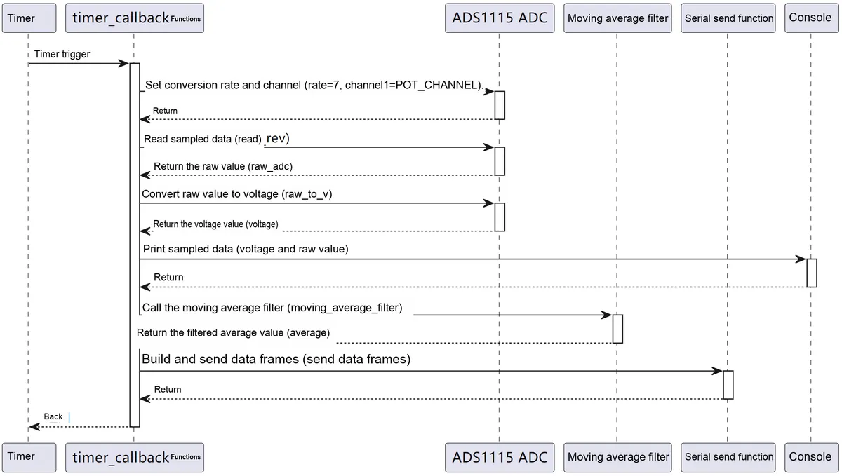
- Set the data rate of the
set_conv ()method toADS1115to7(860 SPS), and the channel toAIN0 - Call the
read_revmethod to read the currentADCconversion result and start the next conversion - Convert the raw
ADCvalues into actual voltage values, and output the voltage value of the current channel and the raw ADC values to the terminal - Call the sliding mean filter function to filter the collected
ADCvalues to reduce the impact of noise - Construct and send data frames, and transmit the filtered
UARTADCdata via it for reception and processing by other devices or computers
Here, the implementation of our moving average filter mainly relies on moving_average_filter function. First, add the new value to the buffer filter_buffer and accumulate it to filter_sum; if the buffer length exceeds the filter window size FILTER_SIZE, remove the oldest value and subtract it from filter_sum. Finally, calculate and return the current moving average to smooth the data through the moving average filter.
In the serial port data frame transmission send_data_frames function, the data frame header 0xAA 0xBB is first constructed, then struct.pack is used to pack raw_adc and average into two 16-bit (<H) data to ensure the correct format during transmission, and the frame header and frame data are concatenated to form a complete data frame to be sent.
Before flashing the code, we need to complete the configuration of the SerialPlot serial port plotter.
- Configure serial port parameters: In the Port tab, select the correct serial port (e. g. COM5), set the baud rate to 256000, data bits to 8, stop bits to 1, and no parity bit
- Click "Open": After confirming that the configuration is correct, click the "Open" button in the upper right corner to open the serial port

- Select Data Format: Switch to the Data Format tab, select the "Custom Frame" format, and set the frame headers to
0xAAand0xBB, with the number of channels set to 2. Since we are transmitting two 16-bit ADC data values, oneADCdata value occupies two bytes, so set theFrame Sizeto a fixed 4 bytes here, set the data type to 16-bit signed number, and select little-endian at the same time
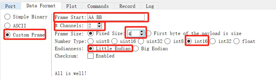
The overall flow of the program is shown in the following figure:
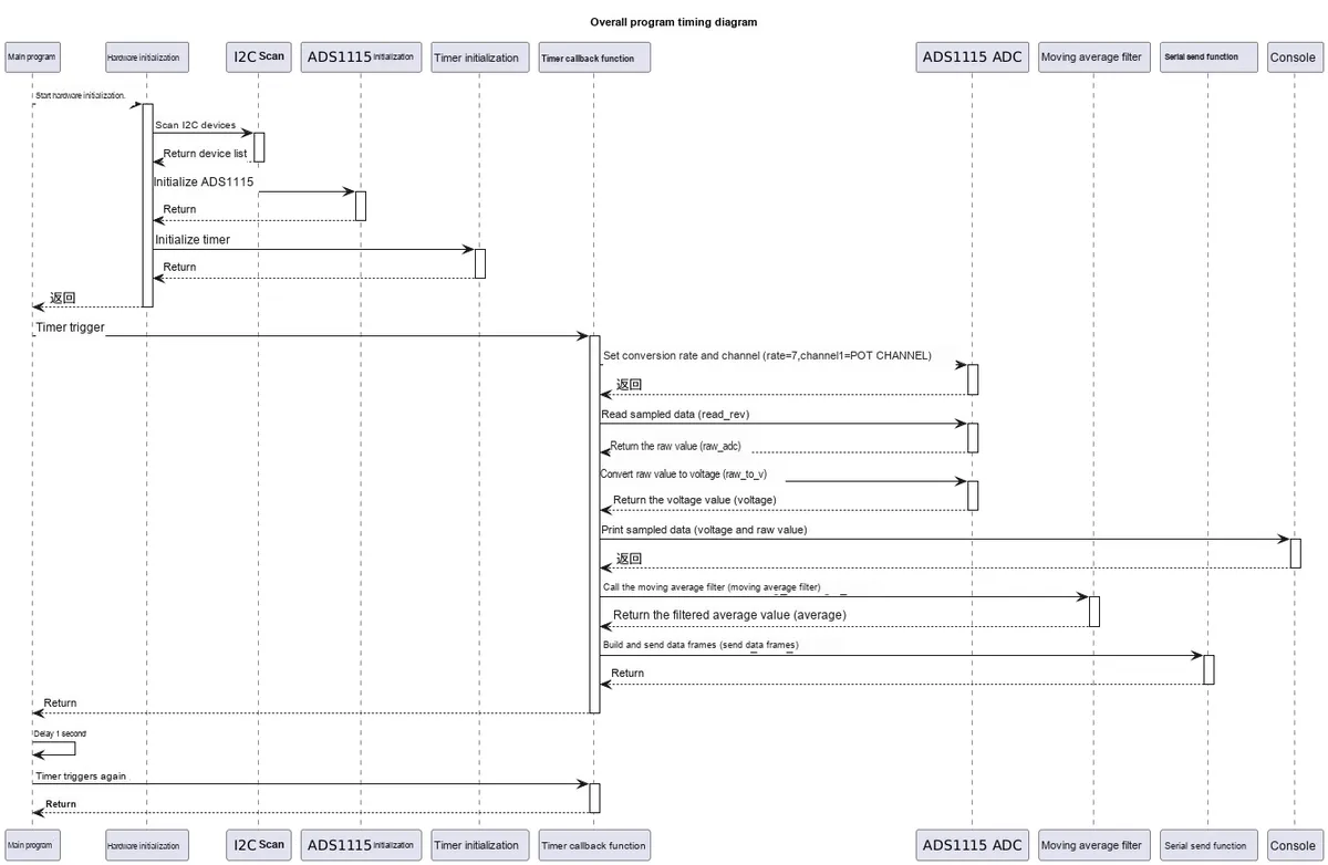
Burn the code, open the terminal, and the following content will be displayed:
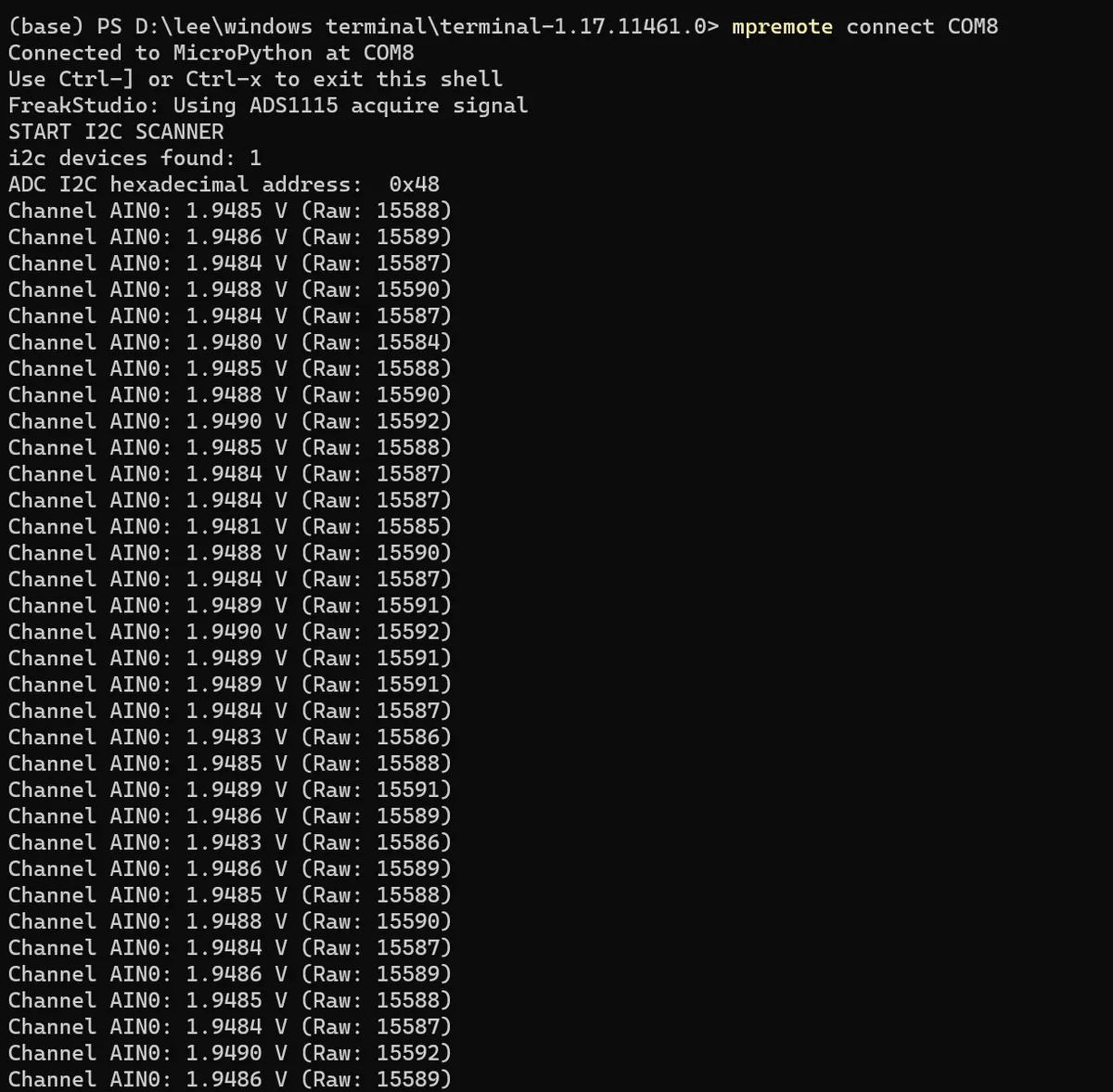
It can be seen that the channel acquisition voltage value is output normally:
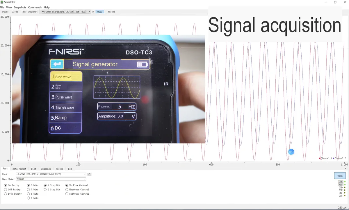
As we adjust different waveforms, the corresponding sampled waveforms also change:
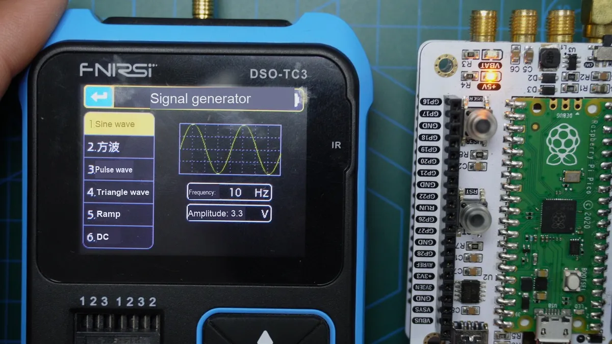
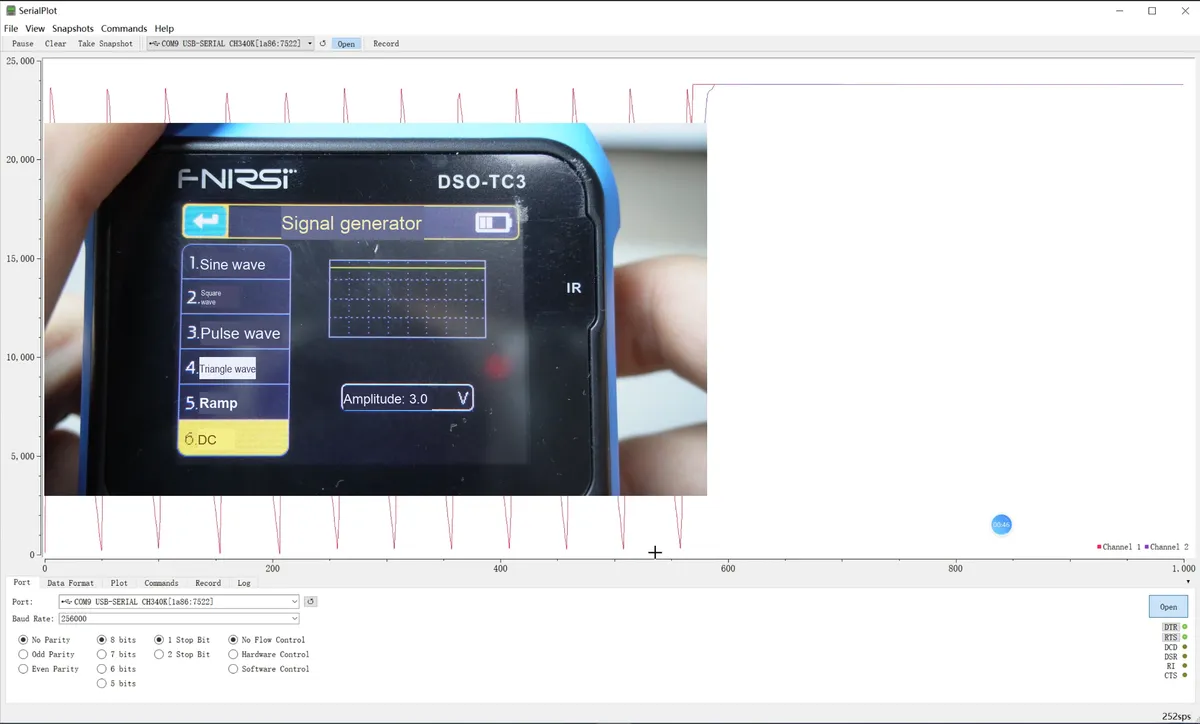
3.5.3 Timer Trigger.mp4 209.3 MB
It can be seen that the red original waveform generated by the DDS signal generator and the blue filtered waveform are normally displayed. The filtered waveform is obviously smoother, but the response speed is slower. It must be noted here that the timer rate must not be greater than the set sampling rate of the ADS1115 chip, otherwise data sampling errors may occur. When using a timer to trigger sampling, the sampling rate is the same as the timer rate; at the same time, according to the sampling theorem, the waveform frequency of the handheld signal generator needs to be less than half of the sampling rate of the ADS1115 chip.
3.4.4 External Interrupt Triggered Sampling of the ADS1115 Chip
In the following code, we use the ADS1115 external ADC chip to acquire the analog voltage output by the signal generator via interrupt triggering. The program communicates with the I2C interface and the ADC, and applies a moving average filter to process the collected raw ADC values. When the ADS1115 chip completes sampling and conversion and triggers an interrupt via the ALERT pin, the code reads the ADC value, converts it to voltage, and sends both the raw and filtered values via the serial port.
When wiring, it is basically the same as the wiring in the timer-triggered ADS1115 chip sampling section, except that ALERT (interrupt output) is connected to the GP13 pin for triggering the interrupt.
The following code can be found in the elegance-devkit v1\Demo\61 ADC_ADS1115_IrqTrigger folder of the resource package we provide.
The sample code is as follows:
# Python env   : MicroPython v1.23.0
# -*- coding: utf-8 -*-
# @Time    : 2024/10/7 2:21 PM
# @Author  : Li Qingshui
# @File    : main.py
# @Description : ADC experiment: use the external ADS1115 ADC chip to collect data, with sampling triggered by an interrupt

# ======================================== Import Modules ========================================

# Import hardware-related modules
from machine import Pin, I2C, UART
# Import time-related modules
import time
# Import the external ADC module
from ads1115 import ADS1115
# Import the module for packing and unpacking binary data and native data types
import struct

# ======================================== Global Variables ============================================

# External ADC address
ADC_ADDRESS = 0
# Channel the rotary potentiometer is connected to: AIN0
POT_CHANNEL = 0

# Variables for the moving average filter
FILTER_SIZE   = 3
filter_buffer = []
filter_sum = 0

# ======================================== Functions ============================================

# Serial data frame packing function
def send_data_frames(raw_adc: int, average: int) -> None:
    """
    Serial send function that sends the raw ADC value and the filtered average.

    Args:
        raw_adc (int): Raw value collected by the ADC.
        average (int): Filtered average value.

    Returns:
        None: This function has no return value.

    Raises:
        Exception: Raised if building or sending the data frame fails.
    """
    # Declare global variables
    global uart

    try:
        # Build the data frame
        # The frame header is 0xAA 0xBB, followed by two 16-bit values in little-endian format
        frame_header = struct.pack('<2B', 0xAA, 0xBB)
        frame_data = struct.pack('<2H', raw_adc & 0xFFFF, average & 0xFFFF)
        frame_full = frame_header + frame_data
        # Send the data frame
        uart.write(frame_full)
    except Exception as e:
        print("Error in send_data_frames:", e)

def moving_average_filter(new_value: int, filter_size: int) -> int:
    """
    Moving average filter.

    Args:
        new_value (int): New sample value.
        filter_size (int): Filter window size.

    Returns:
        int: Current moving average.

    Notes:
        Uses the global variables `filter_buffer` and `filter_sum` to maintain the state of the sliding window.
    """
    # Declare global variables
    global filter_buffer, filter_sum

    # Add the new value to the buffer
    filter_buffer.append(new_value)
    filter_sum += new_value

    # If the buffer exceeds the filter size, remove the oldest value
    if len(filter_buffer) > filter_size:
        removed = filter_buffer.pop(0)
        filter_sum -= removed

    # Calculate and return the moving average
    return filter_sum // len(filter_buffer)

def alert_callback(pin: Pin) -> None:
    """
    ALERT pin interrupt callback function.

    Args:
        pin (machine.Pin): Pin object that triggered the interrupt.

    Returns:
        None: This function has no return value.

    Raises:
        Exception: Raised if reading the ADC value or sending the data frame fails.
    """
    # Declare global variables
    global adc, POT_CHANNEL

    try:
        # Read the raw ADC value from the ADS1115
        raw_adc = adc.alert_read()
        # Convert the raw value to voltage
        voltage = adc.raw_to_v(raw_adc)
        # Print the sampled data (for debugging)
        print(f"irq ADC value: Channel AIN{POT_CHANNEL}: {voltage:.4f} V (Raw: {raw_adc})")

        # Apply the moving average filter
        average = moving_average_filter(raw_adc, FILTER_SIZE)
        # Print the filtered average (for debugging)
        print(f"ADC value after filter: {average}")

        # Build and send the data frame, passing the raw value and the filtered value
        send_data_frames(raw_adc, average)

    except Exception as e:
        print("Error in alert_callback:", e)

# ======================================== Custom Classes ============================================

# ======================================== Initialization ==========================================

# Power-on delay of 3 s
time.sleep(3)
# Print debug message
print("FreakStudio: Using ADS1115 acquire signal in interrupt mode")

# Create a serial port object with the baud rate set to 256000
uart = UART(0, 256000)
# Initialize the uart object with a baud rate of 256000, 8 data bits, no parity, and 1 stop bit
# Set the receive pin to GPIO1 and the transmit pin to GPIO0
# Set the serial port timeout to 100ms
uart.init(baudrate  = 256000,
          bits      = 8,
          parity    = None,
          stop      = 1,
          tx        = 0,
          rx        = 1,
          timeout   = 100)

# Create a hardware I2C instance using the I2C1 peripheral, with a clock frequency of 400KHz, SDA pin 2, and SCL pin 3
i2c = I2C(id=1, sda=Pin(2), scl=Pin(3), freq=400000)

# Start scanning for devices on the I2C bus and return a list of slave addresses
devices_list = i2c.scan()
print('START I2C SCANNER')

# If devices_list is empty, no device is connected to the I2C bus
if len(devices_list) == 0:
    print("No i2c device !")
# If not empty, print the slave device addresses
else:
    print('i2c devices found:', len(devices_list))
    # Iterate over the slave device address list
    for device in devices_list:
        # Check whether the address is between 0x48 and 0x4B; if so, it is an ADS1115 chip address
        if 0x48 <= device <= 0x4B:
            print("ADC I2C hexadecimal address: ", hex(device))
            ADC_ADDRESS = device

# Create the ADC instance with the gain set to 1
adc = ADS1115(i2c, ADC_ADDRESS, 1, alert_pin=4, callback=alert_callback)

# ========================================  Main Program  ============================================

# Start the interrupt-triggered continuous conversion mode of the ADS1115
adc.conversion_start(4,POT_CHANNEL)
# Infinite loop: no specific operation
while True:
    # Delay 1s
    time.sleep(1)
Its main working principle is as follows: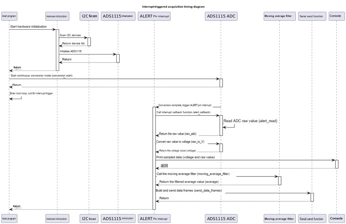
- First, call the
adc.conversion_start ()method, configure the sampling channel and trigger mode to continuous conversion, so that the ALERT pin will be triggered each time the ADS1115 completes data sampling and conversion preparation. - When the ALERT pin is triggered, call the
alert_callback ()function, in which use thealert_read ()method to read the raw value from the ADC, convert it to voltage, print the data, and call the sliding average filter and send the data frame.
Before flashing the code, we need to complete the configuration of the SerialPlot serial port plotter.
- Configure serial port parameters: In the Port tab, select the correct serial port (e. g. COM5), set the baud rate to 256000, data bits to 8, stop bits to 1, and disable parity check
- Click "Open": After confirming the configuration is correct, click the "Open" button in the upper right corner to open the serial port

- Select Data Format: Switch to the Data Format tab, select the "Custom Frame" format, set the frame headers to 0xAA and 0xBB, and set the number of channels to 2. Since we are transmitting two 16-bit ADC data values, and one ADC data value occupies 2 bytes, the Frame Size here is fixed at 4 bytes, the data type is 16-bit signed number, and the little-endian order is selected at the same time.
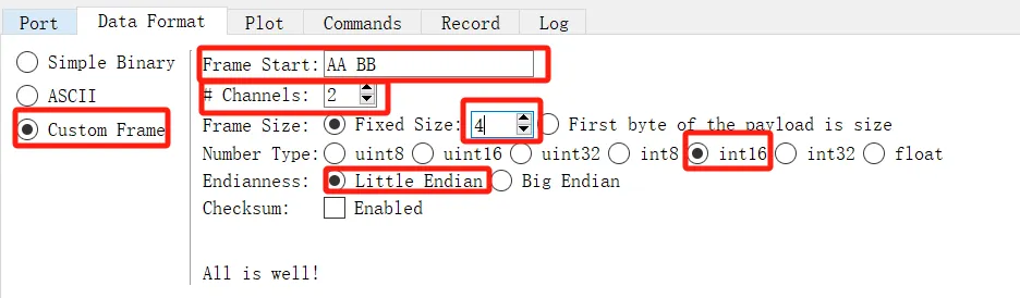
Burn the code, open the terminal, and the following content will be displayed:
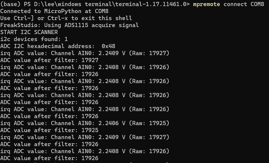
It can be seen that the channel acquisition voltage value is output normally:
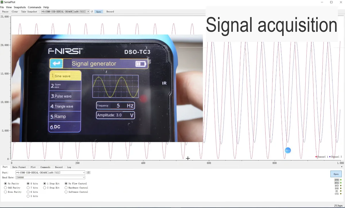
As we adjust different waveforms, the corresponding sampled waveforms also change:
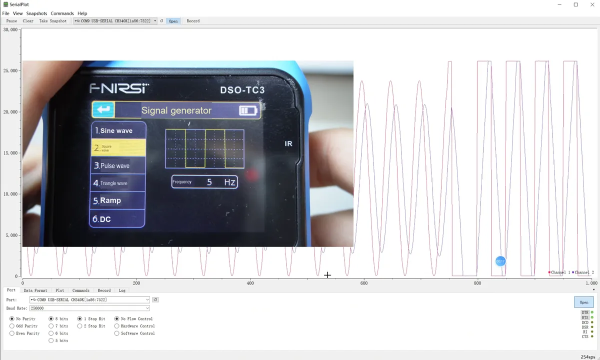
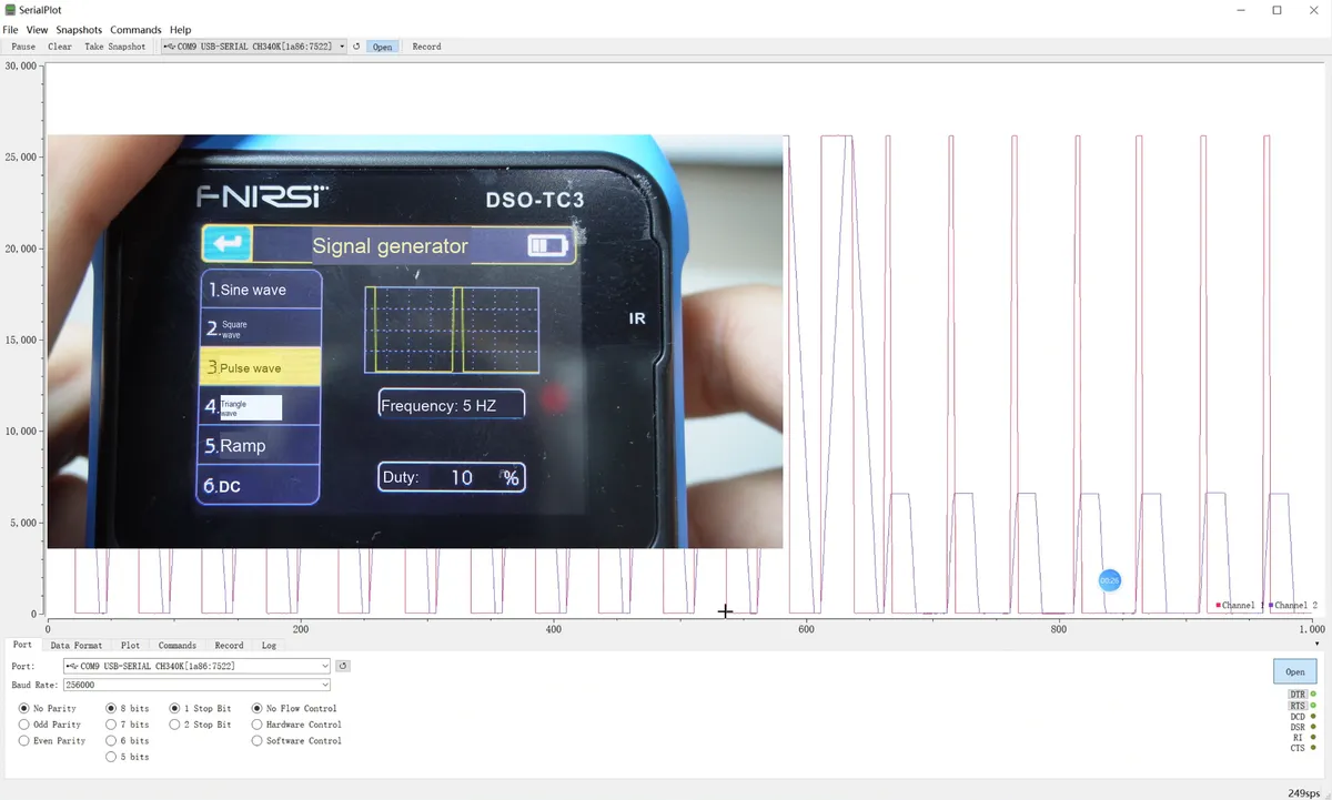
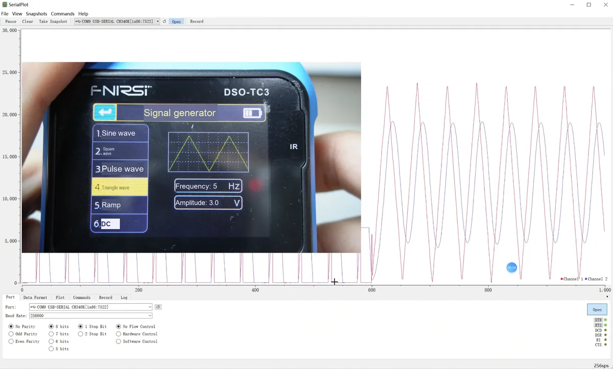
3.5.4 Application Experiment.mp4 85.3 MB
It can be seen that the red original waveform generated by the signal generator and the blue filtered waveform are normally displayed. It should be noted here that when sampling is triggered by an external interrupt, the sampling rate is the same as the set sampling rate of the ADS1115 chip.
References
- Usage of ADC (Analog-to-Digital Converter) on Raspberry Pi Pico
https://pico.nxez.com/2023/08/23/how-to-use-adc-on-the-raspberry-pi-pico.html
- Use the temperature sensor built into the Raspberry Pi Pico
https://pico.nxez.com/2023/09/10/how-to-use-the-temperature-sensor-built-into-the-raspberry-pi-pico.html
- Using a Joystick with the Raspberry Pi Pico
https://pico.nxez.com/2023/11/25/how-to-use-the-joystick-on-raspberry-pi-pico.html
- Raspberry Pico MicroPython: Sampling ADC with trigger and Register Peek and Poke using Inline Assembler
https://forum.micropython.org/viewtopic.php?t=9910&p=55444
- How do Analog to Digital Converters (ADCs) work?
https://www.circuitbread.com/ee-faq/how-do-analog-to-digital-converters-adcs-work
- Analog-to-digital converters basics
https://www.arrow.com/en/research-and-events/articles
- What is an Analog-to-Digital Converter?
https://www.microchip.com/en-us/products/microcontrollers-and-microprocessors
- What Is ADC Converter (Analog-to-Digital Converter)?
https://dewesoft.com/blog/what-is-adc-converter
STM32+ ADS1115 User Manual
https://blog.csdn.net/qq_35654286/article/details/129673810
Driver for the ADS1015/ADS1115 Analogue-Digital Converter
https://github.com/robert-hh/ads1x15
ADS1115 16-Bit ADC Module with Raspberry Pi Pico
https://how2electronics.com/ads1115-16-bit-adc-module-with-raspberry-pi-pico/
Version History
Version Number | Modifier | Time | Content |
v1.0.0 | Li Zisheng | 2025/09/19 | Initialize the document, based on MicroPython version v1.23.0. However, the chapter on high-speed signal sampling has not been written yet. |
v1.0.1 | Li Zisheng | 2025/12/05 | Initialize the document, based on MicroPython version v1.23.0. Some charts and graphs have been modified. However, the chapter on high-speed signal sampling has not been written yet. |
v1.0.2 | 2025/12/23 | Remove the high-speed sampling implemented via ADC inline assembly | |