
Contents
- 1. Hardware Explanation
- 1.1 DAC (Digital-to-Analog Converter)
- 1.2 DDS Signal Generator
- 1.3 External DAC Chip MCP4725
- 1.4 DDS Chip AD9833
- 1.5 Introduction to Digital Potentiometer Chips
- 2. Software Control Method
- 2.1 Custom Class for MCP4725
- 2.2 Custom Class of DS3502
- 2.3 Custom Class of AD9833
- 2.4 Custom Class for MCP41010
- 3. Application Examples
- 3.1 Generating Sine Waves with the MCP4725
- 3.2 Implementing a Waveform Generator with the MCP4725
- 3.3 Implementation of Waveform Generator Based on DS3502
- 3.4 Implementation of Waveform Generator Based on AD9833
- References
- Version History
1. Hardware Explanation
1.1 DAC (Digital-to-Analog Converter)
Digital-to-Analog Converter (DAC) is an electronic device that converts digital signals into analog signals. DACs are widely used in fields such as audio equipment, signal processing, communication systems, and measuring instruments, serving to restore processed digital signals into analog signals.
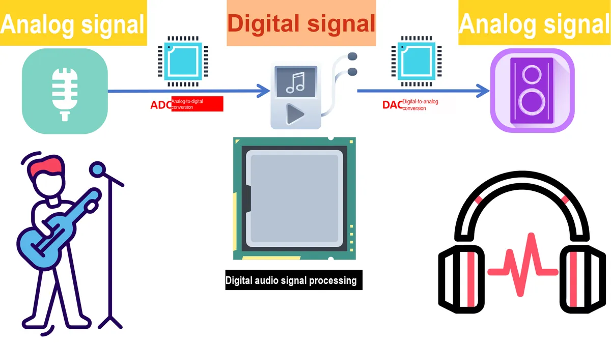
Taking digital audio processing as an example, the DAC (Digital-to-Analog Conversion) unit plays a key role in it, which is responsible for converting the digital signals stored in digital audio files (such as CD, MP3, WAV, etc.) into analog audio signals that can be played through speakers or headphones:
- Recording and Digitization: Audio recording devices use an Analog-to-Digital Converter (ADC) to convert analog signals into digital signals, which are then stored as digital audio files such as WAV or MP3 files.
- Transmission and Processing of Digital Signals: When you play an audio file on a device, these stored digital signals are read and processed by the device's processor; the processed digital signals are then transmitted to the DAC to be converted into analog signals.
- Digital-to-Analog Signal Conversion and Amplification: The DAC receives the processed digital signals, gradually converts these signals into analog voltages whose waveforms are very close to those of the original analog audio signals; the converted analog signals are then sent to an amplifier to boost the signal strength.
1.1.1 Working Principle and Basic Structure of DAC
The input of a DAC is a digital signal composed of 0s and 1s, which is obtained by sampling and quantizing an analog signal with continuous time and continuous amplitude, and its basic constituent units and functions can be mainly divided into three key parts:
- Digital Processing Unit: A digital signal is usually input to a DAC in binary form, with each bit representing a weight of the signal. This unit is responsible for receiving and processing input data from the digital system, and it typically consists of components such as an input register, decoding logic, and control logic.
- D/A Interface (Digital-to-Analog Conversion Interface): This is the core component of a DAC, responsible for converting processed digital signals into corresponding analog signals, a process implemented via resistor networks, current-steering architectures, or other digital-to-analog conversion technologies. Its core function can be summarized as follows: based on the bit weight of each bit, the internal circuitry of the DAC maps these binary bits to corresponding analog levels; the weighted currents or voltages of individual bits are summed into a total current or voltage, which serves as the analog output corresponding to the digital input.
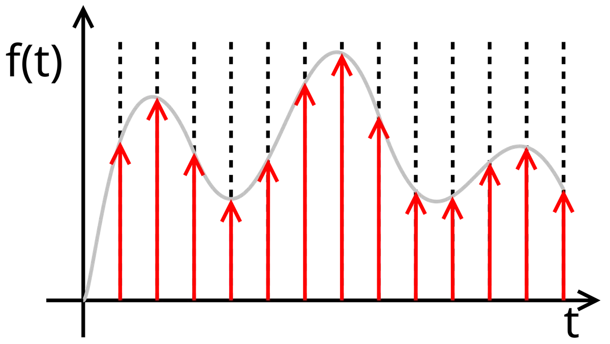
- Reconstruction Filter :The analog signal generated during the digital-to-analog conversion process is typically staircase-shaped (each sampling point corresponds to a fixed voltage or current value). The function of the reconstruction filter is to smooth these staircase-shaped waveforms into a continuous analog signal, eliminate the high-frequency components generated during the conversion process, and it is also used to suppress the aliasing effect that may be introduced during the digital signal conversion process.
In addition, a DAC (Digital-to-Analog Converter) typically further comprises the following components:
- Output Amplifier: The analog signal output by a DAC is usually relatively weak and cannot directly drive loads such as speakers or displays. The output amplifier amplifies this analog signal to an appropriate level to meet the requirements of the load; at the same time, the amplifier also functions as impedance matching to ensure effective signal transmission and reduce signal reflection or distortion.
- Reference voltage: The conversion accuracy of a DAC depends on the reference voltage used internally. The reference voltage provides a stable voltage reference for the DAC's internal circuitry to ensure the accuracy and consistency of conversion results, and it determines the maximum and minimum output levels of the DAC.
- Clock Generation Circuit: The clock generation circuit provides clock signals for the internal digital logic and sampling timing of the DAC, and these clock signals govern the operating frequency and data processing rhythm of the DAC.
1.1.2 Performance Parameters of DAC
The performance of a DAC is mainly determined by the following parameters:
- Resolution: The resolution of a DAC is usually expressed in bits, which refers to the number of discrete voltage or current values it can represent; the higher the resolution, the finer the signals that can be represented. The formula for resolution is 2^N, where N is the number of bits of the DAC. For example, the resolution of an 8-bit DAC is 2^8 = 256
- Sampling Rate: The speed at which a DAC converts and outputs analog signals, usually expressed in conversions per second (SPS, Samples Per Second); the higher the sampling rate, the higher the signal frequency that can be processed, making it suitable for high-speed signal processing.
- Unit Voltage (LSB, Least Significant Bit): the analog signal increment corresponding to the least significant bit (LSB) of a digital signal; LSB determines the precision of a DAC, and LSB =(maximum output voltage - minimum output voltage) / 2^N
- Linearity: The deviation between the actual analog signal output by a DAC and its ideal value, usually expressed as a difference, which mainly includes Integral Nonlinearity (INL) and Differential Nonlinearity (DNL)
- Dynamic Range: The ratio of the maximum amplitude to the minimum amplitude of the DAC output signal, usually expressed in dB; the larger the dynamic range, the wider the range of signals the DAC can process.
- Signal-to-Noise Ratio (SNR): The ratio of the signal output by a DAC to the noise it contains, usually expressed in dB; a higher SNR indicates better quality of the output signal.
- Distortion: The portion of the analog signal output by a DAC that deviates from the original signal, usually caused by non-linearity; the main types include Total Harmonic Distortion (THD) and Intermodulation Distortion (IMD).
1.1.3 Types of DAC
1.1.3.1 Overview of DAC Types
Depending on the implementation approach, DACs come in a variety of structural types. Below are several common structures of DAC digital-to-analog conversion interfaces:
- Weighted Resistor DAC: This type of DAC implements digital-to-analog conversion using a resistor network, where each resistor corresponds to one binary bit (bit). A bit with a higher weight (e. g., the most significant bit) corresponds to a lower resistance value; the digital signal controls whether current flows through each resistor, and finally a corresponding analog current output is generated by superimposing these currents, which is then converted into an output voltage via an amplifier. It features the simplest structure, but requires extremely high precision for the resistors.
- R-2R Resistor Ladder Network DAC: This type of DAC employs a combination of two resistance values, R and 2R, and converts the input digital signal into a corresponding analog voltage signal via the resistor network. Its advantages include easier implementation of resistor matching and lower requirements for manufacturing precision.
- Current-steering DAC: In this structure, digital signals control the switches of a series of current sources, and an analog output signal is generated by adjusting the total current flowing through the load. This structure is suitable for high-speed and high-precision digital-to-analog conversion.
- Integrating DAC: This type of DAC uses an integrating circuit (such as a capacitor and an operational amplifier) to gradually generate an analog signal corresponding to the input digital signal, and is typically used in application scenarios that require high precision but low conversion speed.
1.1.3.2 Working Principle of Digital-to-Analog Conversion Interface for Weighted Resistor DAC
The structure of the digital-to-analog conversion interface of the weighted-resistor DAC is as follows:
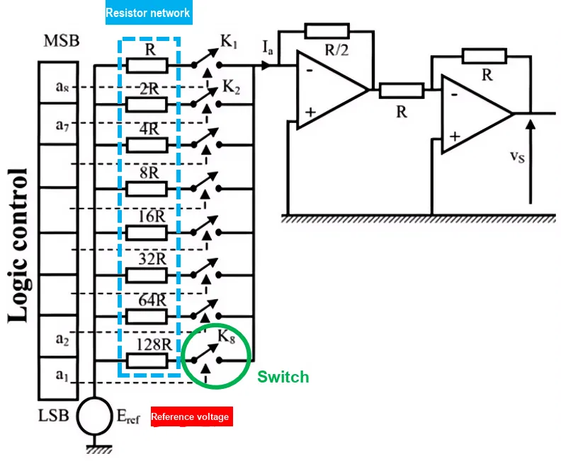
In this structure, it can be divided into three basic parts:
- Reference Voltage: This is the reference voltage provided to the DAC, which is used to determine the amplitude range of the output analog signal.
- Switches: These switches are operated by digital code control logic, and determine which resistors are connected to the circuit according to the state (0 or 1) of the input digital signal
- Resistors: The resistance values in the circuit are weighted and distributed in a geometric progression, such that the current ratio of each resistor is 1/2, which means that the proportion of the current contributed by each resistor in the total output current decreases step by step.
In an 8-bit weighted resistor DAC, the input digital code consists of 8 bits.
Assume that the input digital signal N = 11111111 = a8a7…a2a1
At this point, all switches are in the closed state. Under this condition, the output voltage Vs can be expressed as: Vs = R2 * Ia, where Ia is the current flowing through the resistor, and the total current is:
The final output voltage Vs is:
When the input digital signal N = 01100100, the reference voltage Eref of the DAC is set to 10V. At this time, only switches K2, K3 and K6 are closed, and all other switches are in the open state:
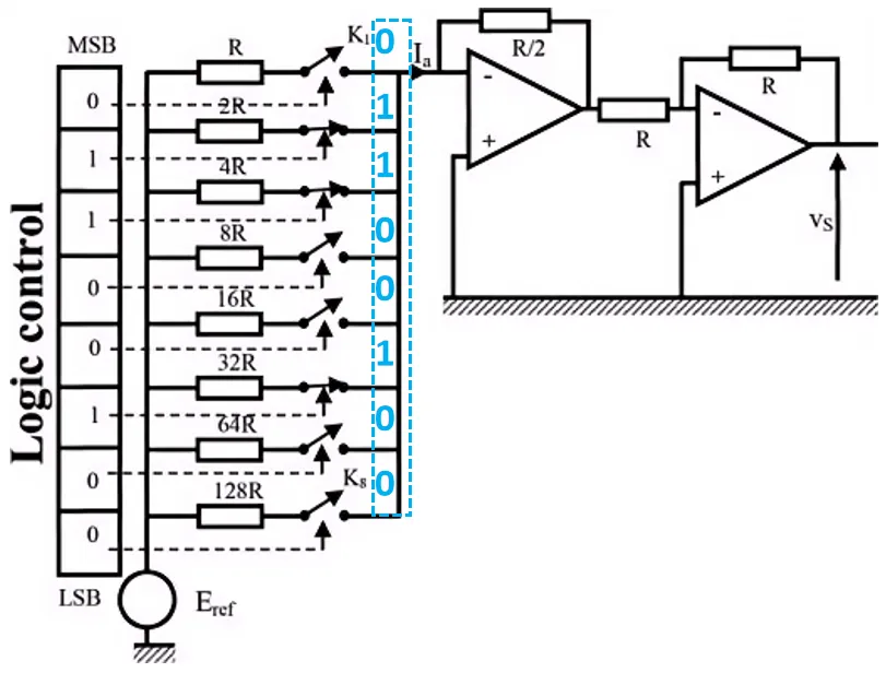
At this point, the corresponding analog output voltage Vs can be calculated using the following formula:
After calculation, the simulated output voltage Vs is obtained as 3.9V.
1.2 DDS Signal Generator
In practical applications, we usually expect to output an analog signal, such as a sine wave or square wave with a set frequency, rather than discrete voltage values. We can use a DAC to output a pre-defined digital signal, but the characteristics such as frequency and amplitude of the signal waveform directly generated by the DAC are usually fixed or limited; if the waveform needs to be changed, it is usually necessary to regenerate and load new digital data, which is a relatively slow process and is not suitable for application scenarios with real-time dynamic changes.
In this case, we can use a DDS signal generator. Direct Digital Synthesis (DDS) is an efficient signal synthesis technology used to generate arbitrary waveform signals such as sine waves, square waves, sawtooth waves and triangular waves. It is widely applied in fields including signal generators, modems, and radio communications. The advantages of DDS lie in its high frequency resolution, fast tuning speed, low phase noise, as well as its flexibility in frequency, phase and amplitude control.
By changing the input parameters of the DDS, the waveform can be adjusted in real time during operation. DDS is suitable for application scenarios requiring frequency synthesis, modulation or phase adjustment, such as wireless communication, radar, etc. In fact, the DAC is a component of the DDS signal generator: the output waveform of the DDS is generated via the DAC, where the DDS is responsible for generating digital phase values and converting them into amplitude values of the waveform, while the DAC takes charge of converting these digital amplitude values into analog signals.
We can use a vivid analogy to illustrate the relationship between the two:
- DDS acts like a conductor of an orchestra, determining the rhythm, tonality and variations of the entire piece. A conductor indicates to the orchestra when to play which musical note through gestures and the score, which is analogous to how DDS determines the frequency and phase of the output waveform via digital signals
- DAC is just like a musical instrument: it plays the actual music in accordance with the conductor's instructions, which is analogous to how a DAC converts digital signals into analog waveforms and ultimately outputs them to speakers or other analog devices.
The core of a DDS signal generator consists of a digital phase accumulator, a waveform memory (Look up table, LUT) and a digital-to-analog converter (DAC):
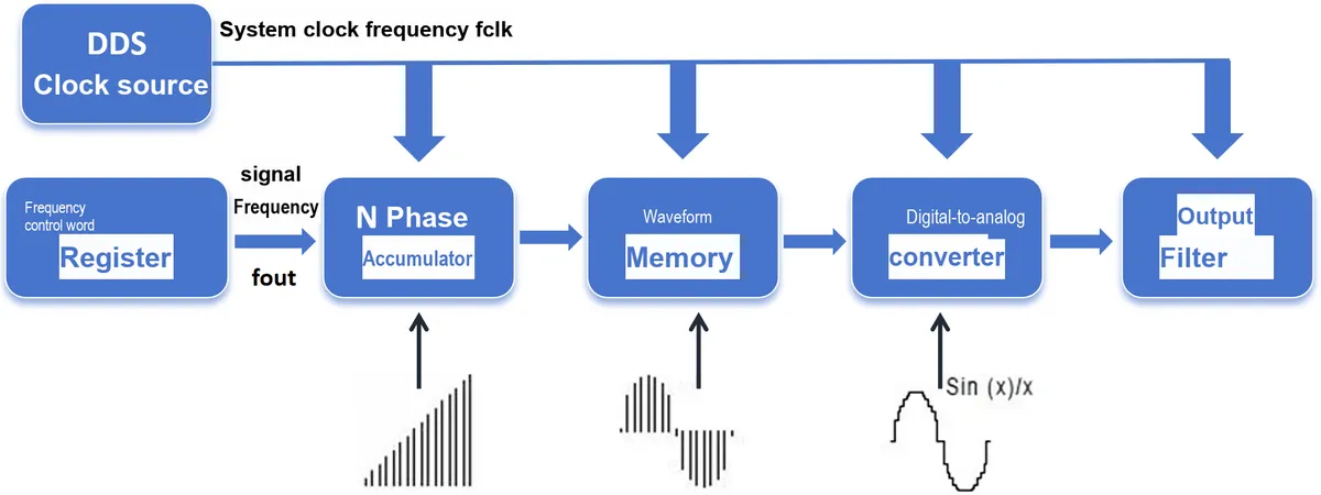
The functions of each component are as follows:
- Clock source: provides the clock signal for the DDS system, usually a stable high-frequency clock; the higher the clock frequency, the higher the frequency resolution and waveform quality of the DDS output signal
- Phase accumulator: a binary adder, usually with a bit width of 32 bits or higher, which accumulates the frequency control word (FCW) into the current phase value in each clock cycle
- Frequency Control Word (FCW) Register: stores the frequency control word, which is used to control the frequency of the output signal; the frequency of the output signal can be quickly changed by modifying the FCW
- Waveform Memory (Look up table): Stores digital waveform data, which are typically the individual sampling points of a sine wave; the size and content of the waveform memory determine the types and precision of waveforms that a DDS can generate.
- DAC (Digital-to-Analog Converter): Converts digital waveform data into analog signals
- Output Filter: Filters the signal output from the DAC to remove high-frequency components and noise, thereby obtaining a clean analog waveform signal.
The following is the working process of DDS:
- Phase accumulation: The main working unit here is the phase accumulator, which is a module based on a modulo-N counter that increments its value by a fixed step size, and the step size for each increment is determined by the Frequency Control Word (FCW)
- Assume that the clock frequency of the system is fclk, then the frequency fout of the output signal can be calculated using the following formula:
where FCW is the frequency control word, and N is the bit width of the phase accumulator
- The output of the phase accumulator is a phase value, which is used to look up the corresponding waveform data in the waveform memory
- Waveform Search:
- The waveform memory stores pre-calculated waveform data, such as the amplitude of each sampling point of a sine wave; the output of the phase accumulator serves as the address of the waveform memory to look up the corresponding waveform data.
- By mapping the output of the phase accumulator to the address of the waveform memory, DDS can generate waveform signals with different phases.
- Digital-to-Analog Conversion: The digital waveform data read from the waveform memory is converted into an analog signal via a DAC and then output to the load
- Output signal: After being processed by the filter, the final analog signal is output.
1.3 External DAC Chip MCP4725
1.3.1 Introduction to MCP4725
The MCP4725 is a single-channel 12-bit digital-to-analog converter (DAC) manufactured by Microchip Technology Inc. , featuring non-volatile EEPROM memory, and it is widely used in applications requiring precise analog signal output, such as audio signal generation, sensor signal conditioning and voltage reference adjustment.
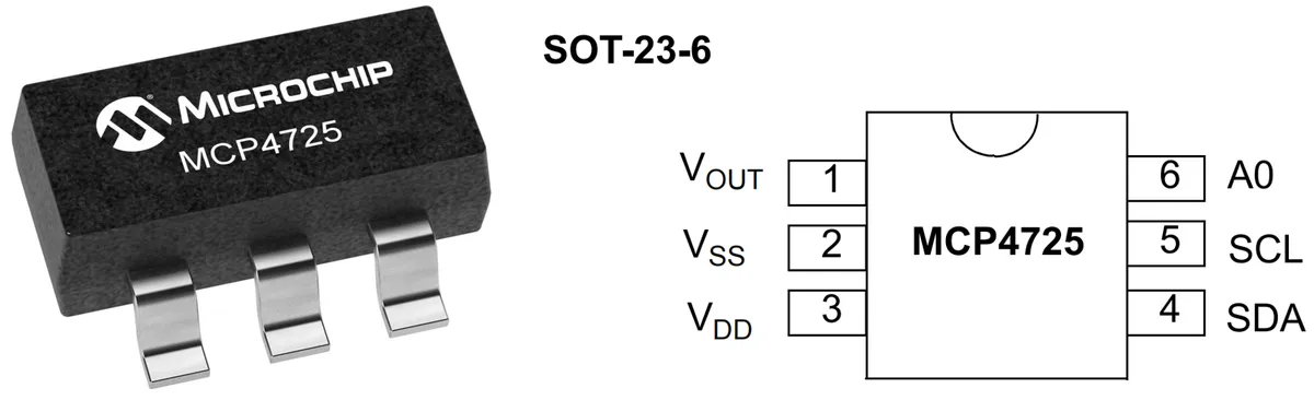
The main features of the MCP4725 are as follows:
- 12-bit resolution: The MCP4725 offers a 12-bit resolution, which means it can output 4096 distinct voltage levels. This makes it suitable for scenarios that require high-precision signal generation.
- I²C Interface: The MCP4725 communicates via the I²C bus, which means it can be easily integrated with master devices such as microcontrollers, and the output of the DAC can be controlled simply by using the I²C Communication Protocol
- EEPROM Storage: This device incorporates an onboard non-volatile EEPROM, which is capable of storing the value of the DAC output register, meaning that the output value will remain unchanged even when the device is powered off or restarted.
- Output Voltage Range: The output voltage range of the MCP4725 is from 0V to Vcc, and the accuracy of the output voltage depends on the reference voltage Vref, which is usually the same as the supply voltage.
- Low Power Consumption: The MCP4725 is a low-power device, making it ideal for battery-powered applications
- Compact Package: It typically adopts the SOT-23 or MSOP-8 package, making it ideal for space-constrained designs.
Its internal structure is as follows:
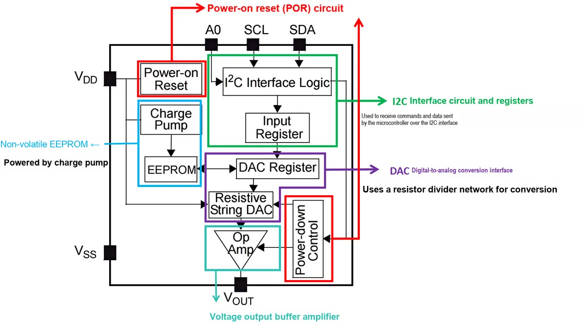
1.3.2 Pin Function Description of MCP4725
The pin functions of the MCP4725 are described as follows:
Pin Name | Description |
VOUT | Analog output voltage: the output terminal of the DAC, which is used to output the converted analog voltage signal, with an output voltage range between GND and VDD. |
VSS | Ground Reference: The ground pin of the DAC, which provides the ground reference for the circuit and is connected to the analog ground of the circuit board. |
VDD | Supply Voltage: This is the power supply pin of the DAC, which provides the required operating voltage. Its input range is from 2.7 V to 5.5 V, and a bypass capacitor is required for filtering. |
SDA | I2C Serial Data: Used for data transmission via the I2C interface. |
SCL | I2C Serial Clock Input: A data synchronization clock signal for the I2C interface. |
A0 | I2C Address Bit Selection Pin: Used to select the I2C address bit of the DAC. It can be connected to VSS (ground) or VDD (power supply), or driven by a digital logic signal; the logic state of the A0 pin determines the I2C address. |
1.3.3 Electrical Parameters of MCP4725
The following is an introduction to the electrical parameters of the MCP4725:
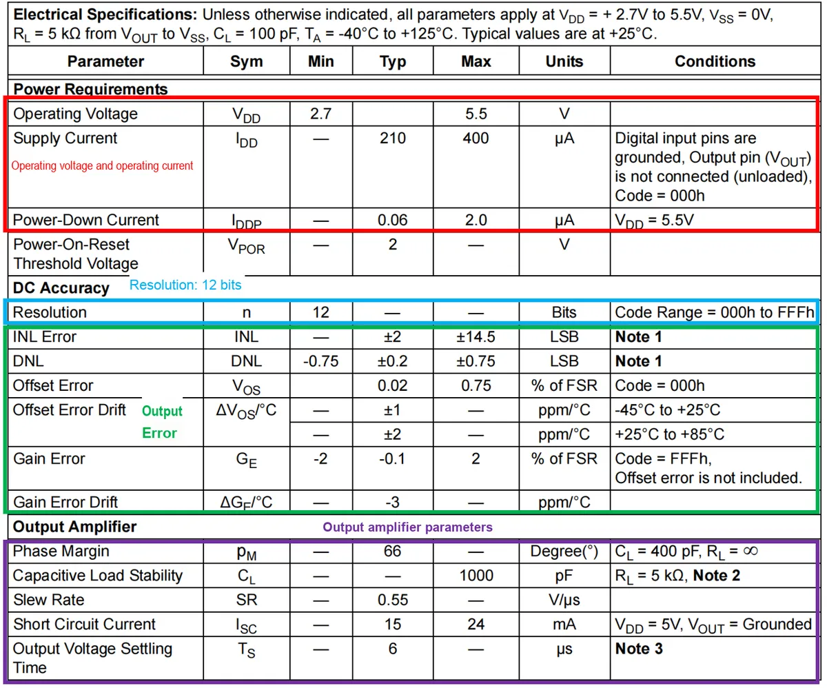
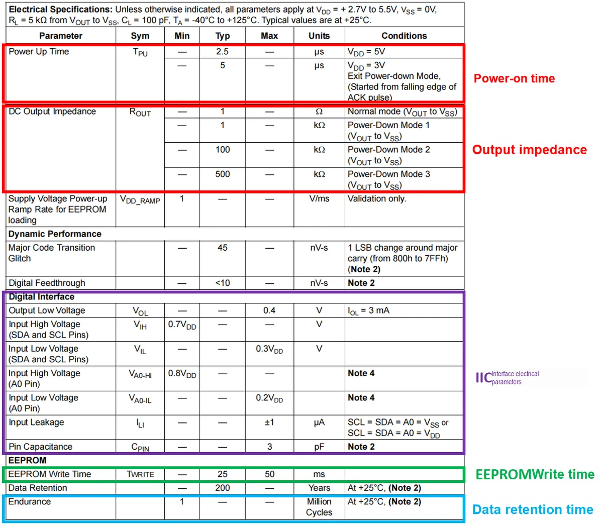
The key parameters are listed as follows:
- Operating Voltage (VDD): The range of power supply voltages within which a DAC can operate normally, from 2.7V to 5.5V.
- Supply Current (IDD): The current consumption of the DAC in normal operation mode, with a typical value of 210 µA.
- Power-Down Current (IDDP): The current consumption of the DAC when it enters the power-down mode, with a typical value of 0.06 µA.
- Integral Non-Linearity Error (INL): the error between the DAC output and the ideal linear output, with a maximum value of ±14.5 LSB, which indicates the linearity of the DAC output; if the INL error is large, the deviation between the DAC output and the expected value will increase.
- Differential Non-Linearity Error (DNL): the error between the analog outputs corresponding to two adjacent digital values, with a typical value of ±0.2 LSB; a smaller DNL indicates that the output variation of the DAC between different digital values is more uniform.
- Gain Error (GE): The error between the actual gain and the ideal gain of the DAC output voltage, with a typical value of -0.1%(maximum 2%); a large gain error may cause the output voltage to deviate from the expected value.
- Output Voltage Settling Time (TS): The time required for a DAC's output voltage to settle from one value to another, with a typical value of 6 µs; a shorter settling time indicates that the DAC can respond quickly to input changes.
- Power-up time: The time required for a DAC to become fully ready after power-on. A shorter power-up time means the device can start operating normally more quickly, which is particularly important in applications that require frequent restarts.
- Resistance Output Impedance (ROUT): The internal resistance at the DAC output terminal. The relatively low output impedance (1 Ω) in normal mode helps stabilize the output voltage, while the high impedance value in power-saving mode affects the load capacity of the DAC output.
- EEPROM write time: the time required to write data to the EEPROM.
- Data Retention Time: The duration for which an EEPROM can retain data without being powered on.
1.3.4 Operating Modes of MCP4725
The device has two operation modes: normal mode and power-saving mode. The mode is selected by programming the power-down bits (PD1 and PD0) in the configuration register, and users can also program these two power-down bits in the non-volatile EEPROM memory.
- Normal Mode: The device performs normal digital-to-analog conversion
- Power-down mode / Energy-saving mode: The device enters an energy-saving state and turns off most of its internal circuits. In the energy-saving mode, all internal circuits (except the I2C interface) are disabled, with no data conversion events and no VOUT output. The output stage switches to a known resistive load, the value of which is determined by the state of the power-down bit. Setting the energy-saving mode can also avoid unnecessary output voltage (e. g., during startup or shutdown).
The setting of the power-off bit is as follows:
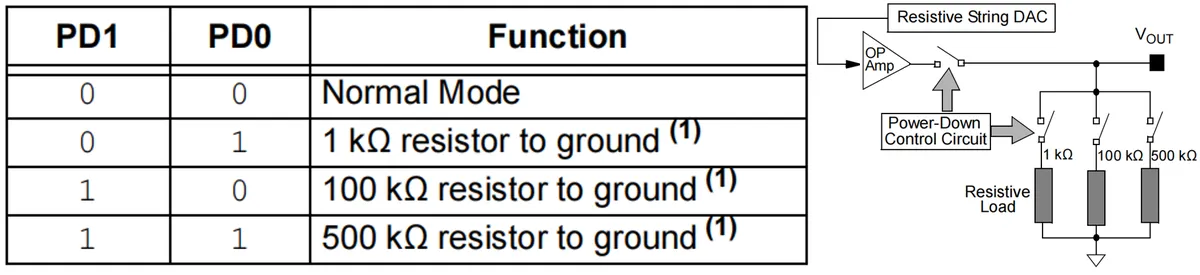
By selecting an appropriate pull-up resistance value, the leakage current at the output terminal in Power-Down mode can be controlled.
1.3.5 EEPROM Storage of the MCP4725
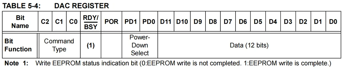
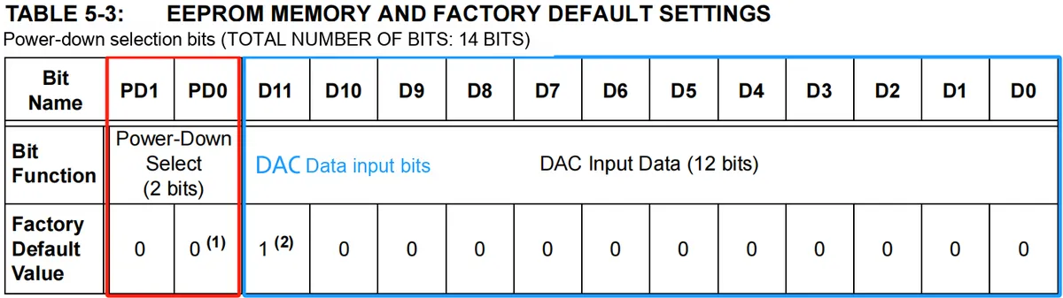
The MCP4725 features a 14-bit wide EEPROM that stores configuration bits (2 bits) and DAC input data (12 bits). These bits can be read from and written to via I2C interface commands. An EEPROM write operation is initiated when an EEPROM write command is received (data bits C2 = 0, C1 = 1, C0 = 1). During the write operation, the RDY/BSY status bit remains low until the write operation is complete. Once the write operation finishes, the RDY/BSY data bit goes high.During the write period, any new write command will be ignored.
1.3.6 Operating Mode of MCP4725
The MCP4725 communicates with the master device (MCU) via the I2C bus and operates as a slave device; the master device can write to or read from the DAC input register or EEPROM through commands via the I2C interface.
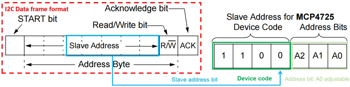
The I2C device address of the MCP4725 consists of four fixed bits (1100 = device code) and three address bits (A2, A1, A0). Among these bits, the A2 and A1 bits are hard-wired during the manufacturing process and are programmed to "00" by default, while the A0 bit is determined by the logic state of the A0 pin.
The A0 pin can be connected to VDD or VSS, or be driven by a digital logic level, as shown in the following figure:
1.3.6.1 Write Command of MCP4725
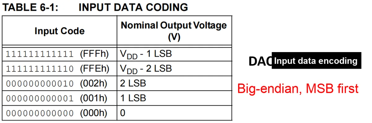
We can input the analog voltage code to be output through the I2C interface. The input code of the MCP4725 is unsigned binary, and the output voltage ranges from 0V to VDD. The formula for calculating the output voltage is as follows:
where D is the DAC input data (ranging from 0 to 4095).
The write command is used to load configuration bits and DAC input codes into the DAC register, or write to the device’s EEPROM; the type of the write command is defined by the three write command type bits (C2, C1, C0).
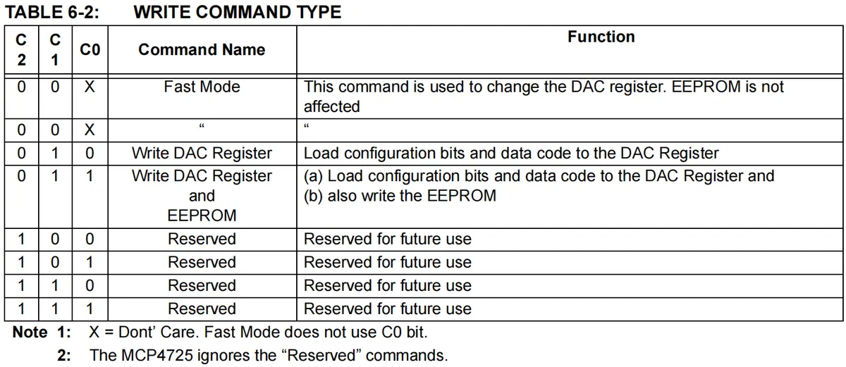
Among these, there are three types of write commands:
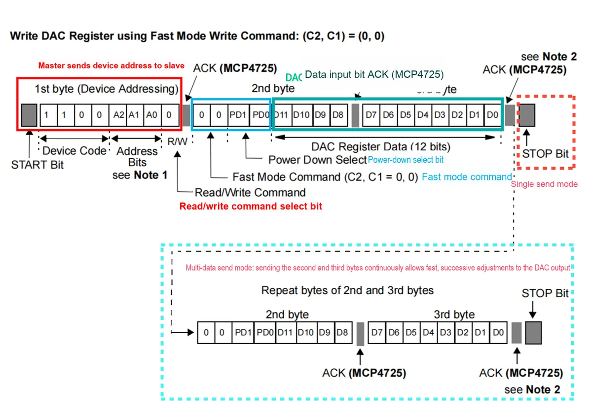
- Fast Mode Write Command (C2= 0, C1= 0, C0= X): The fast write command is used to update the DAC register; the device's EEPROM is not affected by this command. This command updates the power-down mode selection bits (PD1 and PD0) and the 12-bit DAC input code in the DAC register, and the device updates VOUT on the falling edge of the ACK pulse of the third byte:
- We can send a stop bit to terminate the transmission after sending the three-byte command for the first time, thus completing one data transmission.
- It is also possible to send a repeated start bit after transmitting the 3-byte command for the first time, and then send the new second and third bytes of DAC input bytes and power-down selection data bits to implement multiple consecutive update operations.
- DAC Input Register Write Command (C2= 0, C1= 1, C0= 0): This command performs the same function as the fast mode command, but transmits the write command type bits and power-down select bits separately from the DAC input byte. Bits D11 to D0 represent the DAC input data in the third and fourth bytes, and the last 4 bits (X, X, X, X) in the fourth byte are don't care bits. The device executes the master's write command after receiving the last byte (the fourth byte). The master can send a stop bit to terminate the current sequence, or send a repeated start bit to update the data.
- Command for Writing to DAC Input Register and EEPROM (C2= 0, C1= 1, C0= 1): When the device receives this command, it loads the configuration and data bits into the DAC register and writes the data to the EEPROM; while the device is writing to the EEPROM, the RDY/BSY bit goes low and remains low until the EEPROM write operation is completed, and the status of the RDY/BSY bit can be monitored via a read command
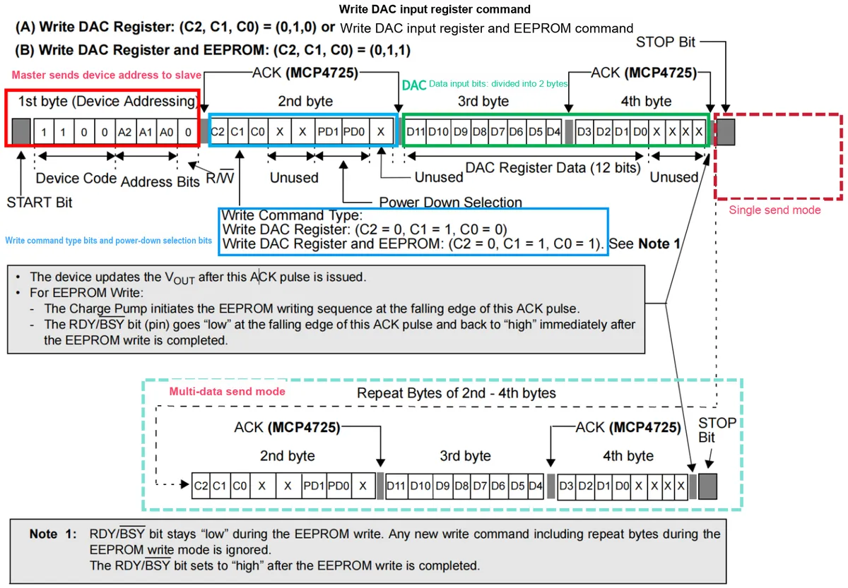
1.3.6.2 Read Command of MCP4725
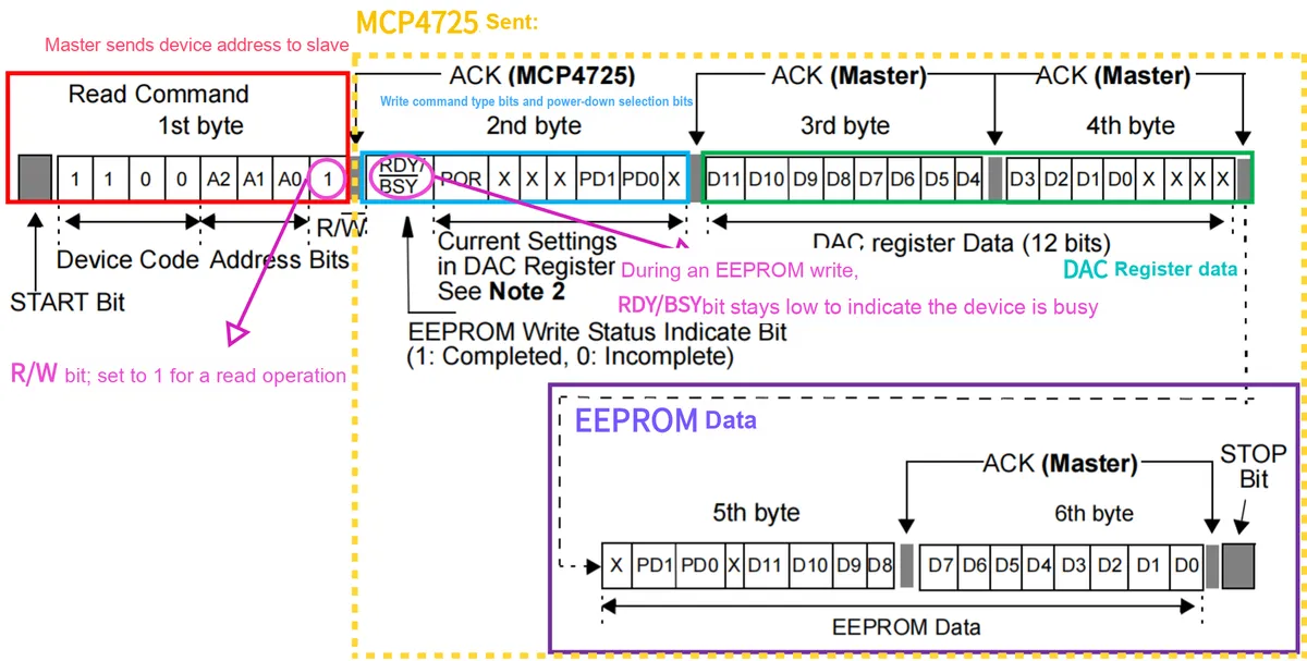
The read command operation flow of the MCP4725 is mainly used to read data from the DAC output register and EEPROM: when the master device sends a command with the R/W bit set to "high level"(i. e., R/W = 1), the MCP4725 will enter read mode and output its current DAC register and EEPROM data on the SDA data line.
1.3.7 I2C General Call and High-Speed Mode of MCP4725
1.3.7.1 Broadcast Call
General Call is a special communication mode in the I2C protocol, which allows the master device to send a General Call Address to all slave devices on the bus for broadcast communication, instead of addressing a specific slave device individually. As a slave device, the MCP4725 supports this General Call and responds to certain specific commands.
The broadcast call address is 0x00, which means that the first byte of the address byte is all zeros, and the function of the broadcast call is determined by the content of the second byte.
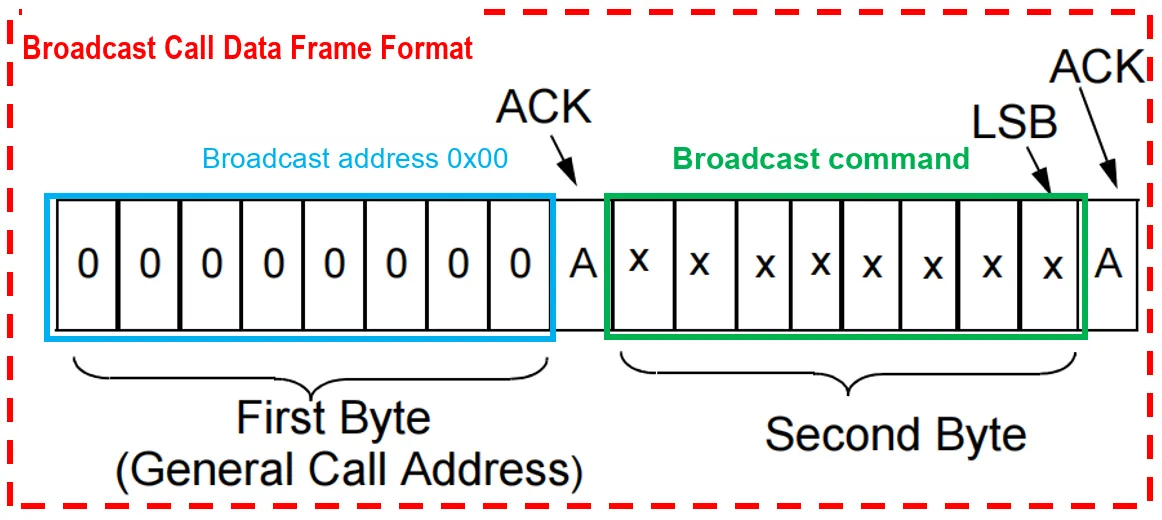
The MCP4725 supports the following two broadcast call operations:
- General Call Reset: The second byte is
00000110(06h). When the MCP4725 receives this command, it immediately aborts the ongoing conversion operation and performs an internal reset, which is similar to a Power-On Reset (POR). After the reset, the MCP4725 reloads the content from the EEPROM into the DAC register and returns to the initial power-on state. - General Call Wake-up: The second byte is
00001001(09h). When the MCP4725 receives this command, it will reset the power-down data bits (PD1, PD2) in the DAC register to the normal operation mode (PD1, PD2 = 0,0), and this operation will not affect the settings of the power-down data bits in the EEPROM.
Multiple MCP4725 devices may be connected to a single I2C bus, and the master device can send a broadcast command to enable all devices to perform a synchronous reset or wake-up, thereby simplifying the system initialization process.
1.3.7.2 High-Speed Mode
High-Speed Mode (HS Mode) is one of the three operating modes supported by the I2C protocol, which enables a faster data transfer rate to accommodate application scenarios requiring high throughput. HS Mode supports a maximum data transfer rate of 3.4 Mbit/s, significantly improving communication efficiency compared to the Standard Mode (100 kbit/s) and Fast Mode (400 kbit/s).
The I2C protocol requires that before entering high-speed mode, a special address byte must be sent 00001XXX to activate HS Mode, where XXX is the unique code of the high-speed master (HS Master). After receiving this address byte, the MCP4725 will not acknowledge (i. e., will not send an ACK), but will switch to HS Mode.
The I2C high-speed mode is commonly used in applications requiring high data transmission rates or multi-device communication, which can reduce bus occupancy time and improve system response speed.
1.3.8 Typical Applications of MCP4725
1.3.8.1 Simple Voltage Output of MCP4725
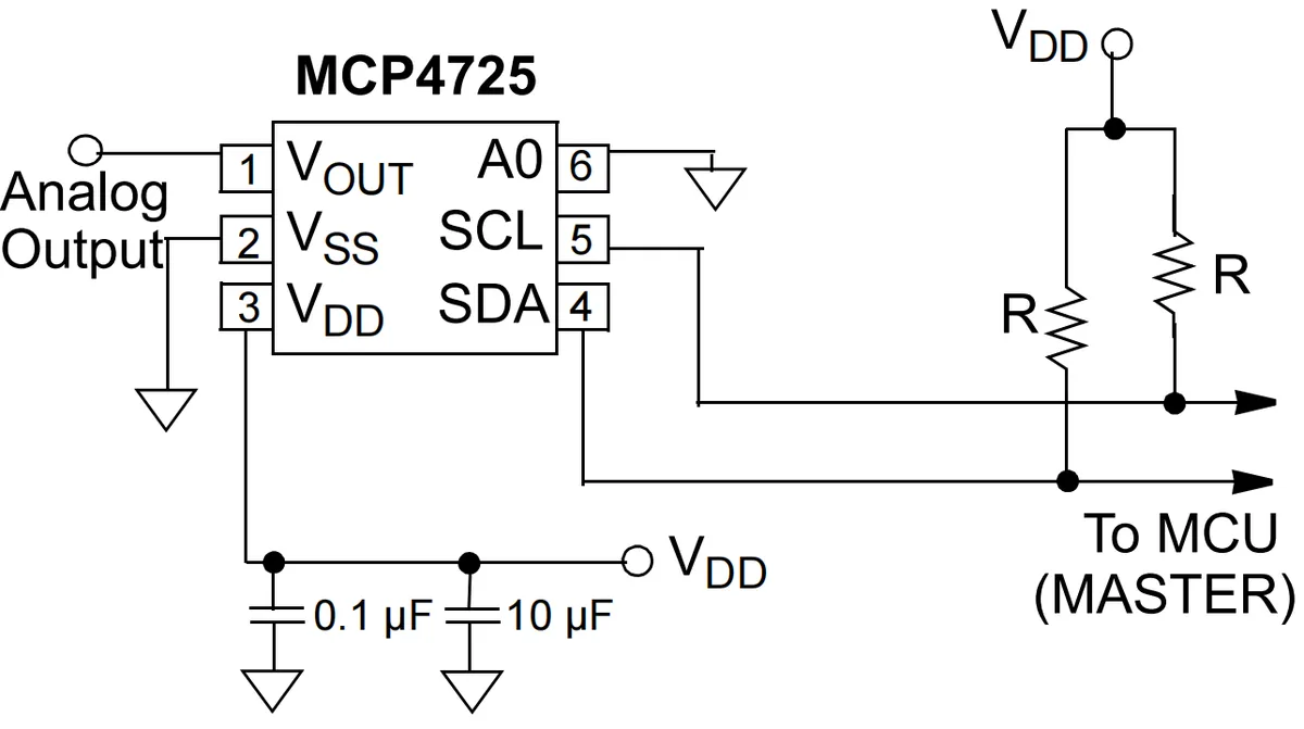
At this point, Vout serves as the analog voltage output; the A0 pin can be connected to GND, VDD, or a digital pin of the microcontroller to set the I2C address, and two pull-up resistors, typically ranging from 1kΩ to 10kΩ, are connected to the I2C communication interface.
Two filtering capacitors are usually connected to the VDD input voltage, typically a 10µF tantalum capacitor and a 0.1µF ceramic capacitor; meanwhile, these capacitors should be placed as close to the VDD pins as possible (within 4mm) during PCB layout.
The schematic diagram of the simple voltage output of MCP4725 is as follows:
1.3.8.2 MCP4725 Reduce Output Step Size
When VDD is 3.3V, the output voltage step of the MCP4725 is 3.3V / 4096 ≈ 0.805 mV. Some applications may require an extremely small DAC output voltage step (e. g., 200 µV), which can be achieved by using a voltage divider at the DAC output. The voltage divider scales down the DAC's output step while mitigating the impact of noise.
The following circuit is used for precise detection of optical sensor signals and fine adjustment of output voltage, and it is applied to detect whether the light intensity reaches the set threshold:
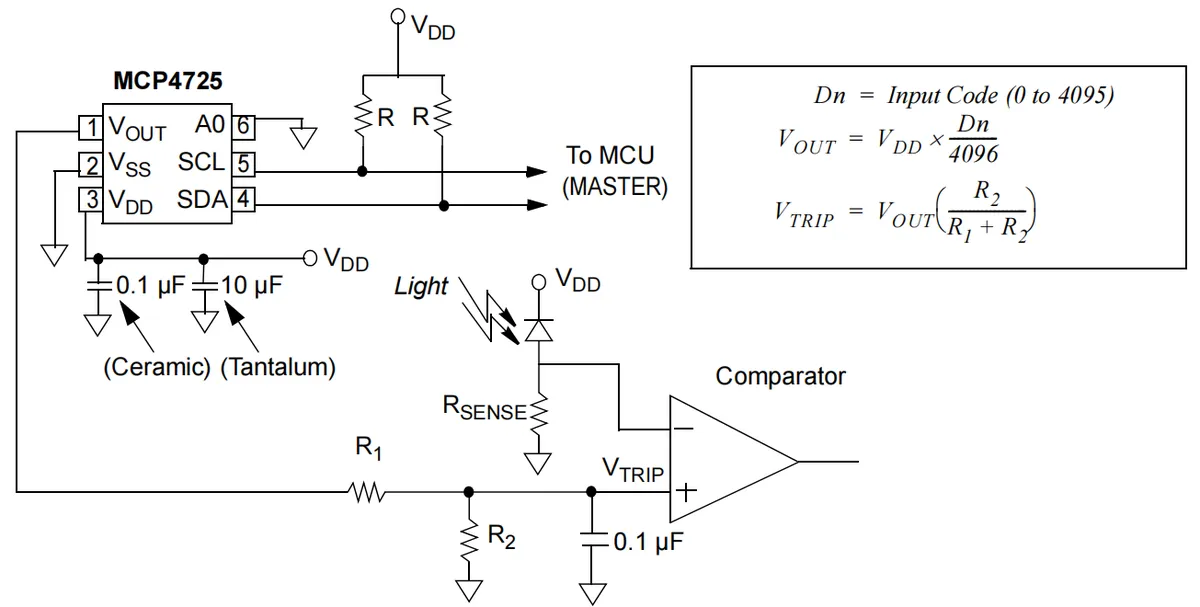
Wherein, R1 and R2 form a voltage divider, which is used to adjust the output voltage VOUT of the DAC to a lower voltage VTRIP, and the calculation formula for VTRIP is as follows:
The other end of the comparator is connected to a sensing resistor (RSENSE) and a photodiode. This resistor is used to sense the current flowing through the photodiode; under illumination, the photodiode generates a current, which creates a voltage drop across RSENSE. The comparator is used to determine VTRIP and RSENSE the voltage difference across them, thereby generating a corresponding output signal. The comparator can be used to detect whether the light intensity or the current exceeds a preset threshold.
1.3.8.3 MCP4725 Builds a "Window" DAC
For sensor applications requiring extremely high resolution around a setpoint or threshold voltage, a "window" DAC can be constructed using a voltage divider network with pull-up and pull-down resistors, which significantly improves step resolution while narrowing the output voltage range.
The following circuit is used to detect whether the current in the circuit exceeds the safe range:
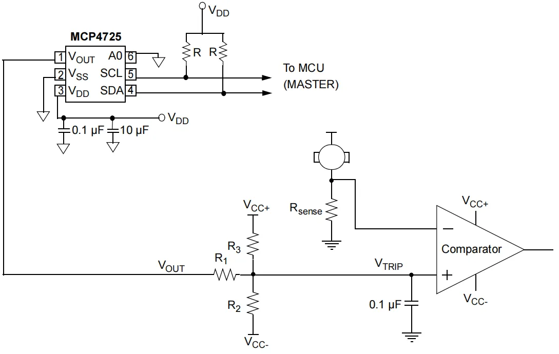
Wherein, the analog voltage generated by the MCP4725 according to the input digital code Dn VOUT is given by:
R1, R2 and R3 form a voltage divider circuit that converts VOUT into the input voltage of the comparator, VTRIP. For the convenience of analysis, the circuit can be simplified to a Thevenin equivalent circuit, and the calculation formulas for its equivalent resistance and voltage are as follows:
The voltage finally input to the comparator VTRIP is:
Current-sensing resistor Rsense is used to measure the current flowing through the load. It compares the voltage drop caused by the current with VTRIP to determine whether the current has reached the set threshold.
1.3.8.4 Bipolar Voltage Output of MCP4725
By using an external operational amplifier, the MCP4725 can achieve bipolar operation. This configuration allows users to realize almost any desired output voltage range, power and noise performance by selecting appropriate resistance values. The gain of the op-amp is determined by resistors R1 and R2, while R3 and R4 are used to adjust the output offset of the DAC.
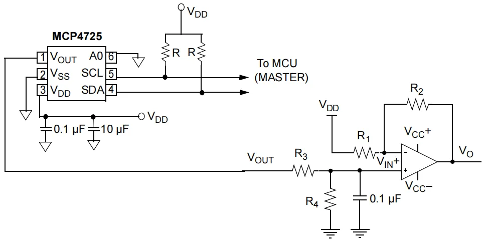
Among these components, the operational amplifier circuit is used to buffer and amplify the output signal of the MCP4725; R1 and R2 form an adjustable gain circuit that allows users to select an appropriate gain, while R3 and R4 are used to shift the output voltage of the DAC to the required bias level.
If a higher bias voltage is required, R4 can be connected to VDD instead of VSS, and a pull-up resistor can be used to replace R4 at the same time.
1.3.8.5 Current Output of MCP4725
By adding a voltage follower and a sensor resistor, the voltage output from a DAC can be converted into a digitally selected current source. This type of circuit is commonly used to drive LEDs, lasers, or other loads that require a stable current supply. By programming the voltage output of the DAC, the current flowing through the load can be precisely controlled.
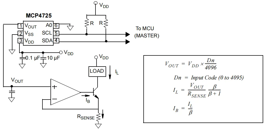
Among them, the operational amplifier supplies different base currents to the triode under different voltages, thereby regulating the current flowing through the load; by measuring Rsense, the operational amplifier adjusts its output to ensure that the current remains constant.
1.4 DDS Chip AD9833
AD9833 is a low-power direct digital synthesis (DDS) chip manufactured by Analog Devices, Inc. Designed for applications requiring precise frequency and phase control, it is capable of generating sine, triangle, and square waveforms, and is commonly used in scenarios such as signal sources and test equipment.
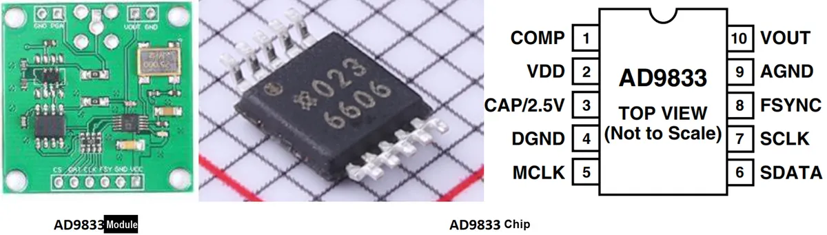
It has the following characteristics:
- Frequency and Phase Programming:
- Frequency Range: 0 MHz to 12.5 MHz
- Phase Programming: Provides phase control, enabling precise phase adjustment of signals
- Power consumption: At a supply voltage of 3 V, the power consumption is only 20 mW
- resolution:
- It uses a 28-bit frequency register to deliver a frequency resolution of up to 0.1 Hz (based on a 25 MHz reference clock)
- When using a 1 MHz reference clock, it can provide a frequency resolution of 0.004 Hz
- Output waveform: Supports sine wave, triangular wave and square wave output
- Power Requirements: Operating power supply voltage range: 2.3 V to 5.5 V
- Interface: Communicates via a 3-wire SPI interface, supports clock speeds up to 40 MHz, and is compatible with DSP and microcontroller standards
- Power Management: Equipped with a power-down function (SLEEP), which can power down unused sections to reduce power consumption; for example, the DAC section can be powered down when generating a clock output.
1.4.1 Basic Structure of AD9833
The basic structure of AD9833 is shown in the following figure:
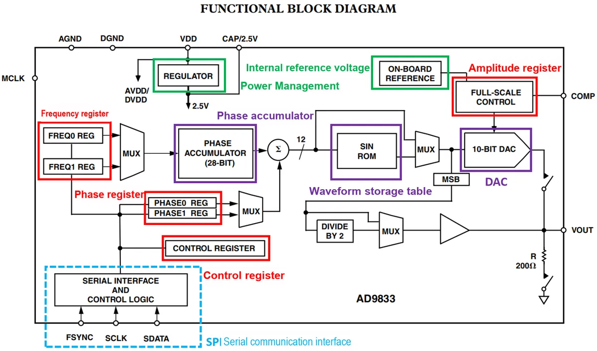
Wherein:
- Frequency Registers (FREQ0 REG and FREQ1 REG): used to set the frequency of the generated output signal
- Phase registers (PHASE1 and PHASE0): used to generate phase signals
- Multiplexers (PHASE MUX and FREQ MUX): used to select the outputs of the frequency register and the phase register
- Phase accumulator: A 28-bit digital accumulator is used to continuously accumulate the frequency control data (FREQ0 REG and FREQ1 REG) over time.
- Waveform storage table: stores the values required for generating waveforms
- DAC (Digital-to-Analog Converter): A 10-bit DAC is used to convert digital signals into analog signals for output.
- Power Management Unit (REGULATOR and ON-BOARD REFERENCE): consisting of a voltage regulator and an internal reference voltage (2.5V)
- Amplitude Register (FULL-SCALE CONTROL): Used to adjust the amplitude of the output signal
- Serial Interface Control Register (SERIAL INTERFACE AND CONTROL LOGIC): provides serial interface and control logic, which is used to configure and control various functions of the chip
1.4.2 Electrical Parameters of AD9833
The electrical parameters of the AD9833 are as follows:
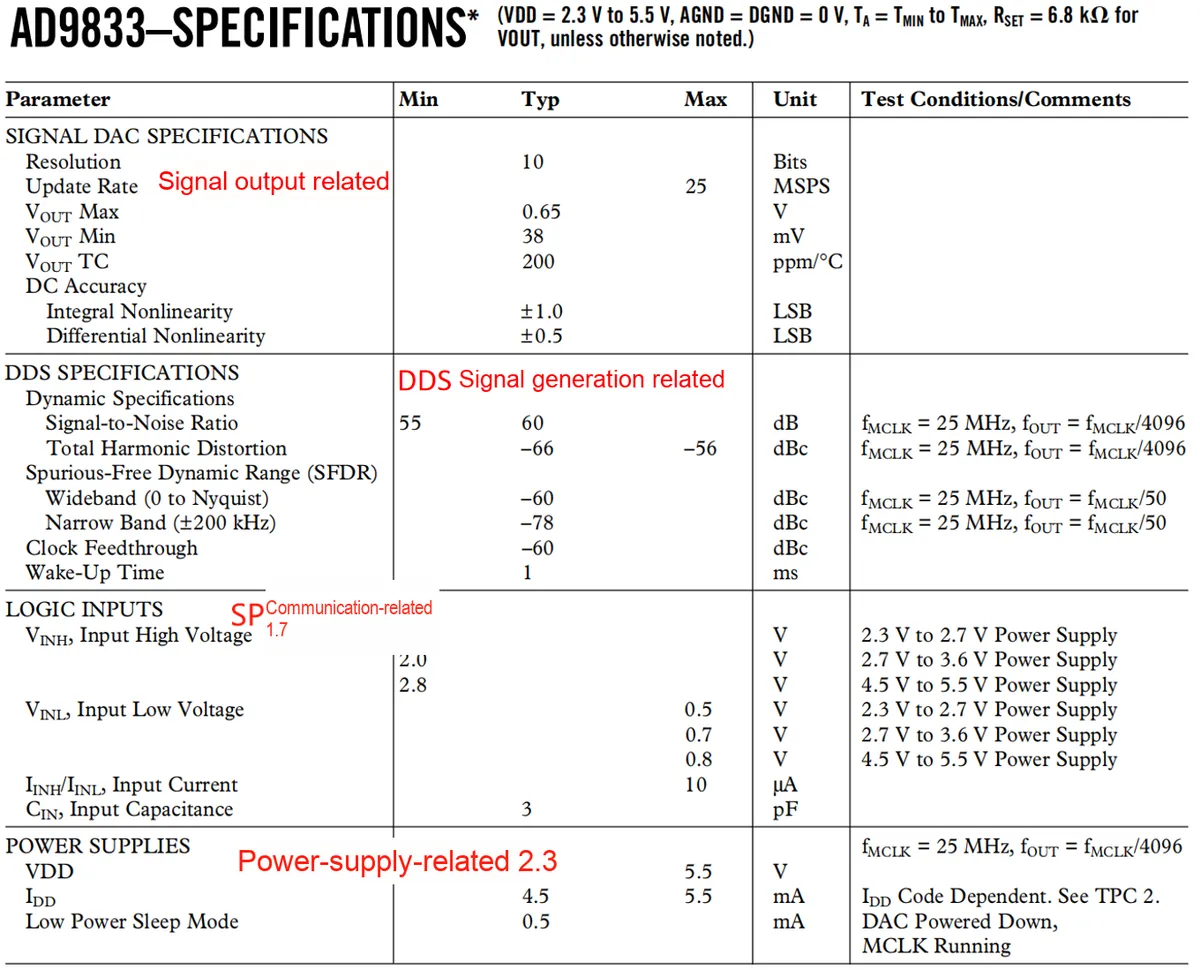
Wherein, the electrical parameters can be divided into the following four parts:
- Parameters related to signal output: The DAC used in AD9833 is 10-bit, with a maximum sampling rate of 25 million samples per second, a maximum output voltage of 0.65 V, and a minimum output voltage of 38 mV; the output voltage is affected by temperature changes, with a temperature coefficient of 200 ppm/°C; the linearity error includes an integral non-linearity error of ±1.0 LSB and a differential non-linearity error of ±0.5 LSB
- Parameters related to DDS signal generation: The signal-to-noise ratio ranges from 55 to 60 dB, the total harmonic distortion is between -66 and -56 dBc, the spurious-free dynamic range (SFDR) is -60 dBc in the wideband range, and -78 dBc in the narrowband range (±200 kHz)
- SPI communication related parameters: The input high voltage and low voltage vary with the power supply voltage. The input high voltage (VINH) ranges from 1.7 V to 2.8 V, the input low voltage (VINL) ranges from 0.5 V to 0.8 V, the maximum input current IINH/IINL is 10 mA, and the input capacitance is 3 pF
- Power supply related parameters: The input power supply voltage ranges from 2.3 V to 5.5 V, and the operating current ranges from 4.5 mA to 5.5 mA; in the low-power sleep mode, the DAC is turned off and the MCLK remains running, and the operating current drops to 0.5 mA
1.4.3 Pins and SPI Communication Parameters of AD9833
1.4.3.1 Pin Description of AD9833
The pins of the AD9833 are shown in the following figure:
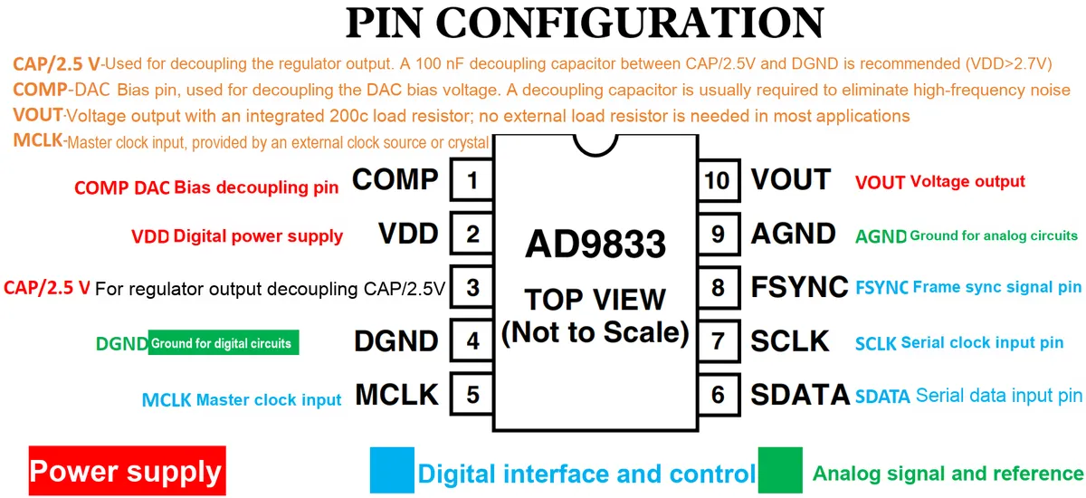
The pin numbers and functions are shown in the following table:
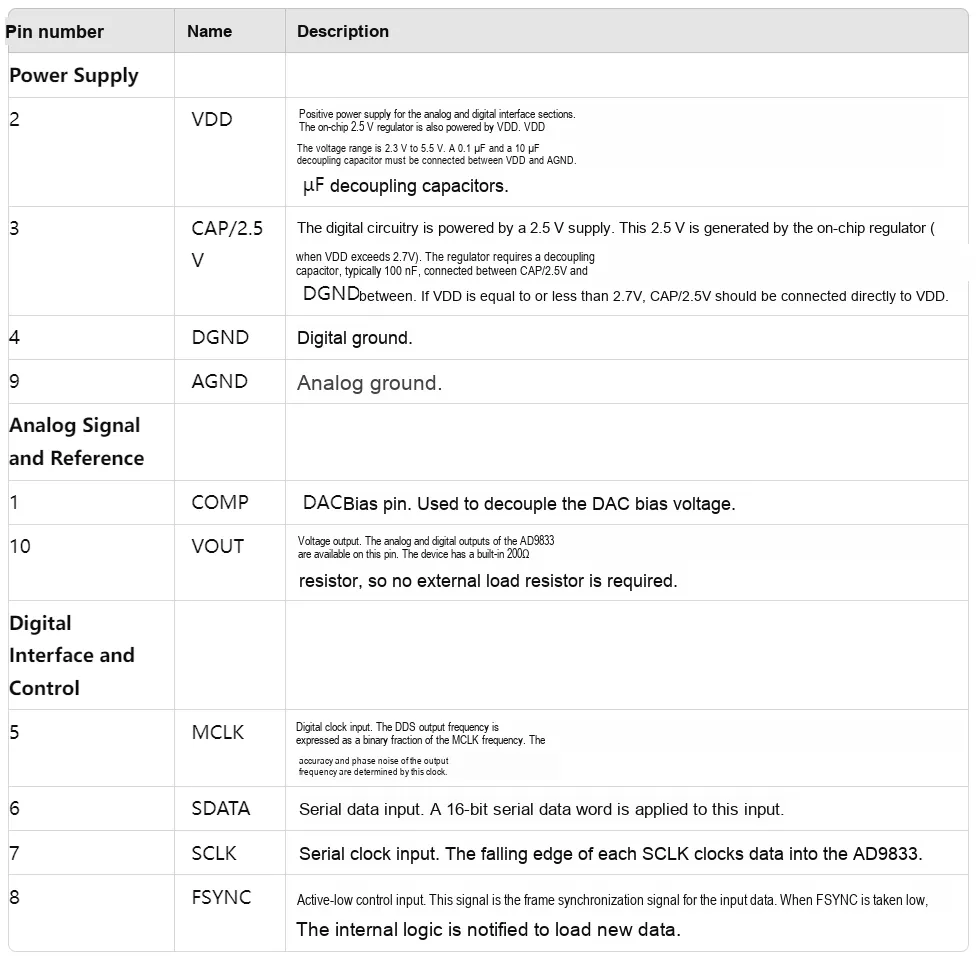
1.4.3.2 SPI Communication Electrical Parameters and Procedure of AD9833
The SPI timing characteristics are shown in the following table:
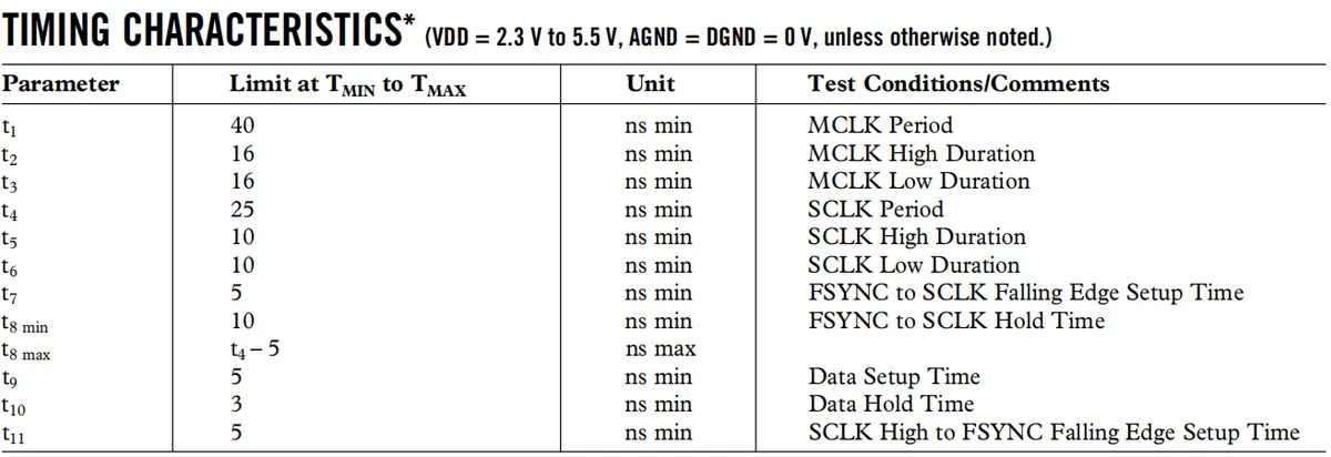
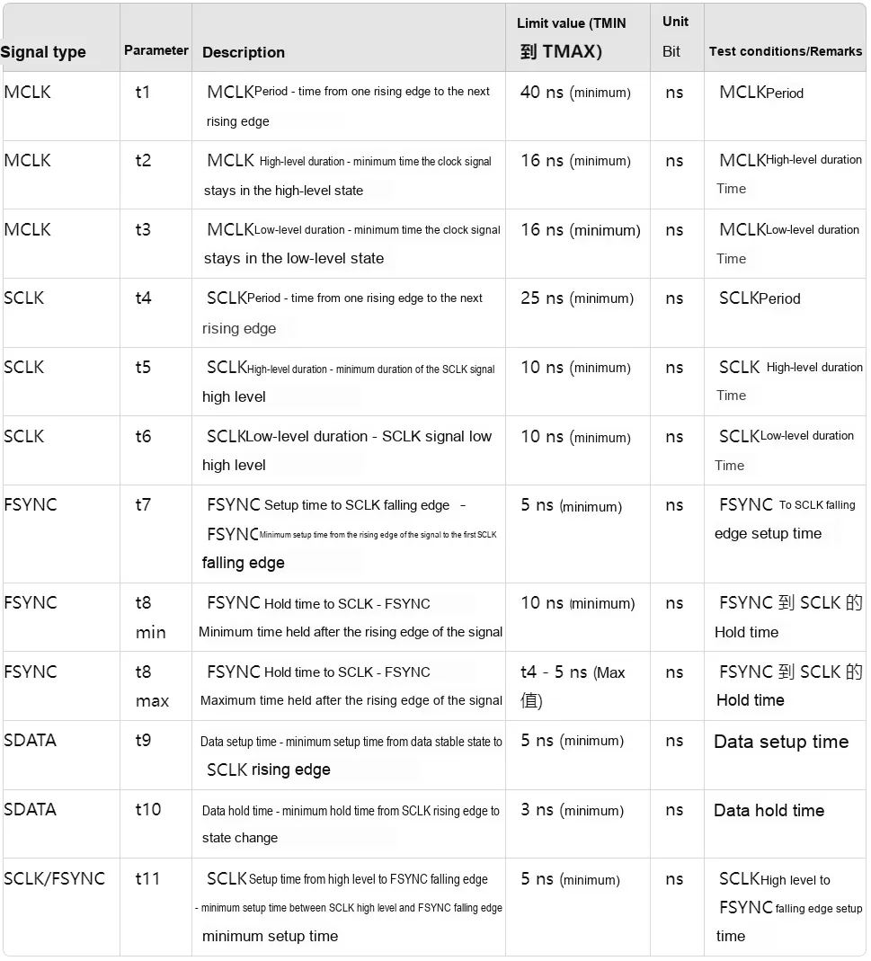
The meanings of the parameters are as follows:
The SPI Sequence Diagram is as follows:
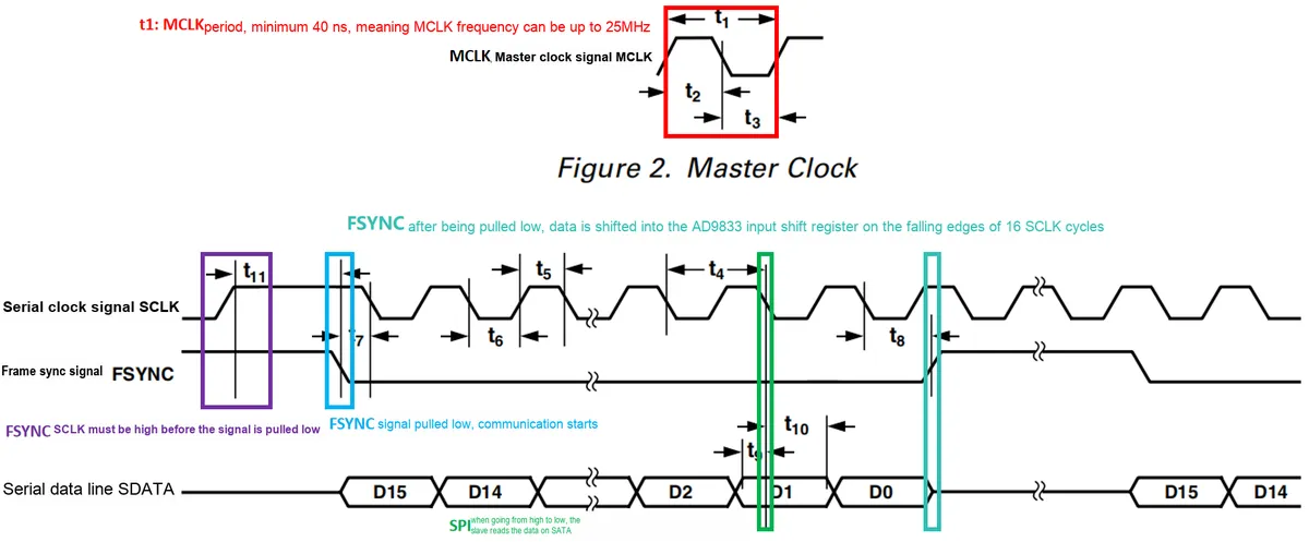
Here, we will first explain the four signals and timing parameters:
- Main Clock Signal: MCLK is the main clock signal input to the AD9833 chip, which defines the operating speed of the system; the minimum period t1 of MCLK is 40 ns, which means the maximum frequency of MCLK can reach 25 MHz, while the minimum high-level duration t2 and low-level duration t3 are both 16 ns.
- Serial Clock Signal: SCLK is the serial clock signal that controls the sampling and transmission of data. Each SCLK cycle corresponds to the transmission of one data bit on the SDATA line. The minimum duration of a complete SCLK cycle t4 is 25 ns, which means the maximum frequency of SPI communication can reach 25 MHz. The minimum duration of the high level t5 and low level t6 of the SCLK signal is 10 ns.
- Frame Synchronization Signal: FSYNC is the frame synchronization signal used to mark the start of a data frame. The minimum setup time t7 from the falling edge of FSYNC to the first falling edge of SCLK is at least 5 ns. The minimum hold time t8 from the rising edge of FSYNC to the last falling edge of SCLK is 10 ns, and the maximum hold time t8 is the SCLK period t4 minus 5 ns.
- Serial Data Line: SDATA is the serial data line used for transmitting data bits; the minimum setup time t9 for data from a stable state to the falling edge of SCLK is at least 5ns, the minimum hold time t10 for data from the falling edge of SCLK to state change is at least 3ns, and the setup time t11 from the high level of SCLK to the falling edge of FSYNC is at least 5ns
Here, the AD9833 adopts three-wire SPI communication with the host, and its communication process can be summarized as follows:
- Communication Start:
- When the master device starts transmitting data, it pulls FSYNC low to enable communication, at which point the AD9833 is ready to receive data.
- The master device generates the SCLK clock signal, which is used to control the timing of data transmission.
- Data Transmission:
- After FSYNC is pulled low, the input shift register of the AD9833 starts receiving data, and each falling edge of SCLK triggers the transmission of one data bit on the SDATA line.
- Data is transmitted serially, and a total of 16 SCLK cycles are required to transmit a complete data packet.
- Data Retention and Transmission Termination:
- After the transmission of 16-bit data is completed, the FSYNC signal can be pulled high to mark the end of one data transmission.
- If multiple packets are to be transmitted consecutively, FSYNC can be held low to transmit multiple 16-bit data in succession, and FSYNC will only be pulled high after the 16th falling edge of SCLK of the last packet.
- After each loading of new data, the AD9833 needs to wait for 7 to 8 MCLK cycles before the output waveform undergoes corresponding changes.
It should be noted that the SPI communication mode of this chip adopts CPOL = 0 and CPHA = 1, namely SPI Mode 1. Moreover, FSYNC (frame sync) does not keep a low level all the time like the standard SPI chip select (CS); instead, it is pulled low briefly before each frame of data transmission. SCLK starts transmitting data only after FSYNC goes low, and cannot run with continuous clocks as standard SPI does. Its protocol is more similar to I²S, TDM, or the SPI variants specific to certain DSP devices.
Simply put, before each data write operation, we need to manually pull SCLK high and then pull the chip select pin low to initiate communication.
1.4.4 Control of AD9833
1.4.4.1 AD9833 Control Register
The AD9833 incorporates a 16-bit control register, which is used to configure the operating mode of the chip.
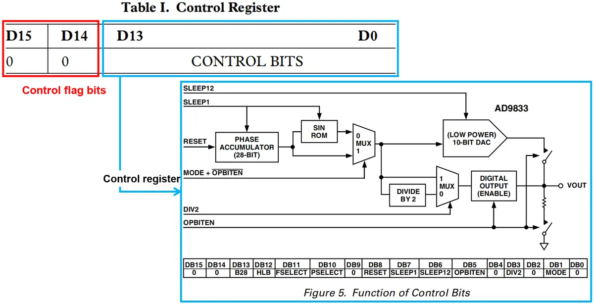
The control register consists of control flag bits and control bits. When a user needs to modify the content of the control register, they must first set both the high-order bits D15 and D14 of the register to 0.
The definitions of the individual control data bits (bits) of the control register are as follows:
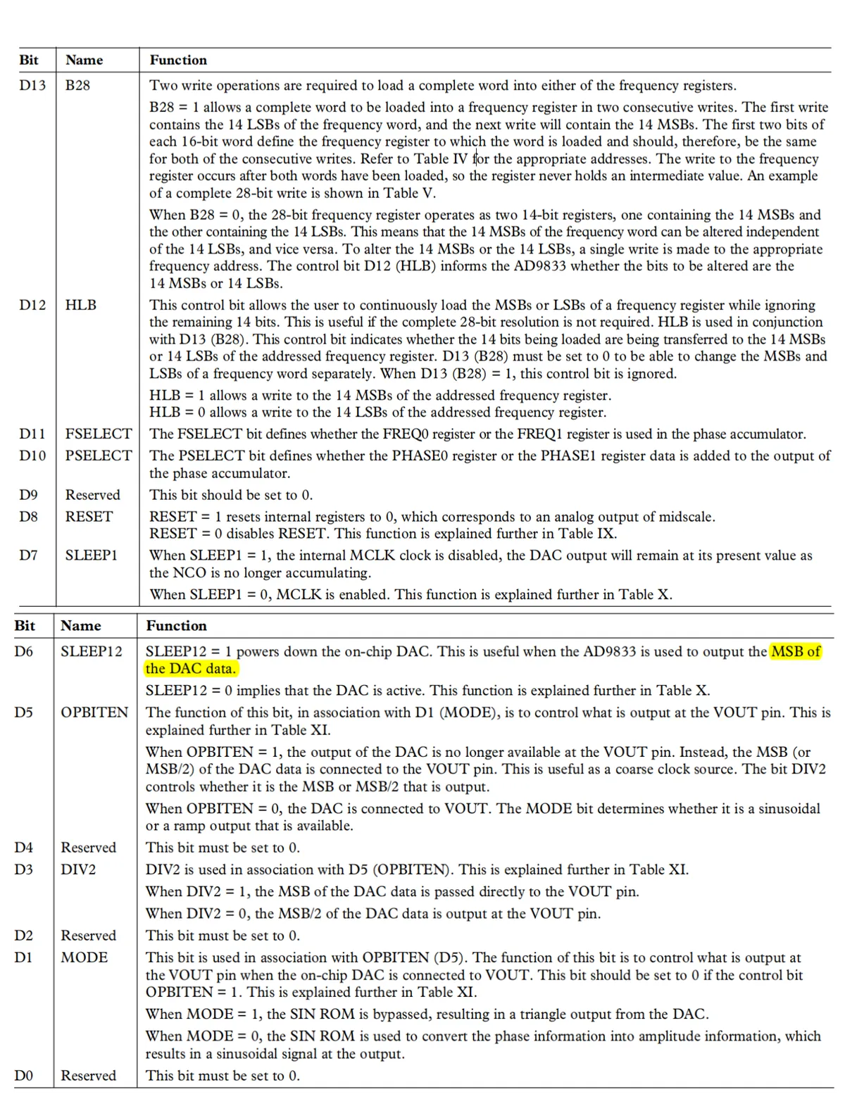
Simply put, the meaning of each bit is as follows:
- D13 (B28): Write mode of the control frequency register
- When B28 = 1, the frequency register requires two consecutive write operations to complete the entire 28-bit frequency word.
- When B28 = 0, the upper 14 bits (MSB) or the lower 14 bits (LSB) can be written separately.
- D12 (HLB): Used to select the upper 14 bits or lower 14 bits of the write frequency register, valid when B28 = 0
- D11 (FSELECT): Select the frequency register for the phase accumulator; 0 selects FREQ0, and 1 selects FREQ1
- D10 (PSELECT): Select the phase register for the output of the phase accumulator; 0 selects PHASE0,1 selects PHASE1
- D8 (RESET): Resets internal registers to 0, sets the output analog signal to the midpoint value; output signal generation starts when RESET = 0
- D7 (SLEEP1): When SLEEP1 = 1, the internal MCLK clock is disabled, and the DAC output maintains the current value
- D6 (SLEEP12): When SLEEP12 = 1, the DAC on the chip is turned off
- D5 (OPBITEN): Used in conjunction with D1 (MODE) to control the output of the VOUT pin. When OPBITEN = 1, the DAC output is no longer connected to the VOUT pin, but to the MSB or MSB/2 of the DAC data; the D3 (DIV2) bit determines whether the output is the MSB or MSB/2
- D3 (DIV2): Used in conjunction with D5 (OPBITEN)
- When DIV2 = 1, the MSB is directly output to the VOUT pin.
- When DIV2 = 0, the MSB/2 output
- D1 (MODE): Used in conjunction with OPBITEN to control the output of the VOUT pin
- When MODE = 1, the SIN ROM is bypassed and a triangular wave is output.
- When MODE = 0, the phase information is converted into amplitude information via the SIN ROM, and a sine wave signal is output.
Each time data is written, the operation starts with writing to the control register; the upper two bits of the 16-bit data written each time are used to determine the register to be written. The initialization workflow for controlling the AD9833 can be summarized as follows: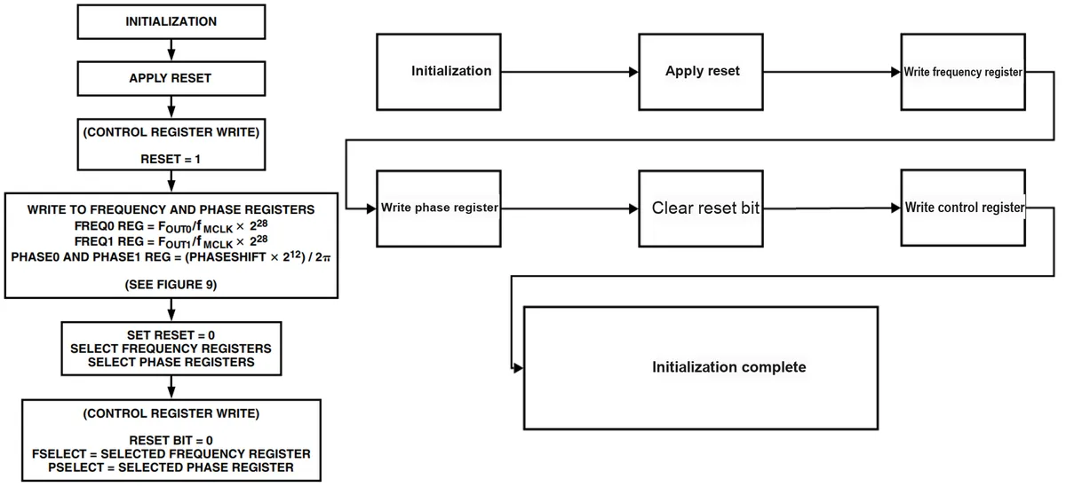
- Power-on reset: Upon power-up, the RESET bit is set to 1, and it is ensured that the data in the frequency, phase and control registers are at known values
- Configure registers: Set each bit in the control register as required. After configuring the control register (with the control flag bits set to '00'), configure other registers to select an appropriate output mode (sine wave, triangular wave, or square wave), and configure the frequency and phase registers (with the control flag bits set to other values)
- Start output: Clear the RESET bit and start outputting the signal
1.4.4.2 AD9833 Frequency and Phase Registers
The AD9833 contains two frequency registers and two phase registers internally, which are used to control the frequency and phase of the output signal:
- Frequency Register:
- FREQ0 (28 bits): When the FSELECT bit is 0, the FREQ0 register determines the frequency of the output signal, and the output frequency is proportional to the MCLK frequency
- FREQ1 (28 bits): When the FSELECT bit is set to 1, the FREQ1 register determines the frequency of the output signal, and the output frequency is proportional to the MCLK frequency.
- Phase Register:
- PHASE0 (12 bits): When the PSELECT bit is 0, the content of the PHASE0 register will be added to the output of the phase accumulator to determine the phase offset of the output signal.
- PHASE1 (12 bits): When the PSELECT bit is 1, the content of the PHASE1 register will be added to the output of the phase accumulator to determine the phase offset of the output signal
The writing process of the frequency register and the phase register is as follows:
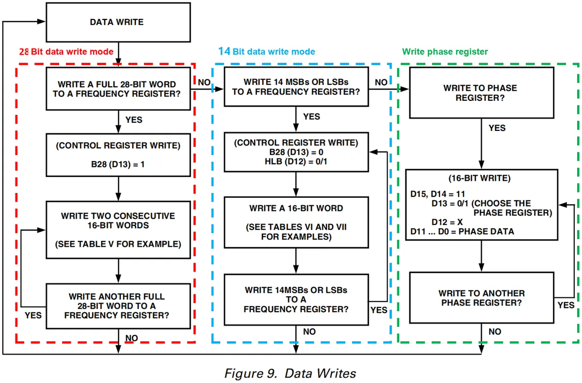
When writing to the frequency register, we can select either the 14-bit data write mode or the 28-bit data write mode. The frequency register write mode can be selected by setting the B28 (D13) data bit and the HLB (D12) data bit in the control register, followed by writing the frequency value. Next, we need to write to the phase register: first, set the D15 data bit and D14 data bit in the control register to indicate that data is to be written to the phase register, then set the D13 data bit to select the target phase register (PHASE0 or PHASE1), and finally write the phase value to it.
1. Writing to the frequency register
The frequency register stores 28-bit binary data, which determines the frequency of the output signal. The frequency calculation formula is as follows:
Wherein, FREQREG is the value in the selected frequency register, fMCLK is the clock frequency, and fOUT is the frequency of the output signal.
Since the frequency register is 28 bits wide while the SPI interface can only transmit 16 bits of data at a time, two write operations are required to write to one frequency register. When it is necessary to modify the entire content of the frequency register, the B28 bit (D13) of the control word should be set to 1, so that all 28 bits of the frequency register can be written in the two write operations.
The writing sequence is as follows:
- Step 1: Transmit the lower 14 bits of data in the frequency register
- Step 2: the upper 14 bits of data in the transmission frequency register
If only partial data needs to be updated, you can choose to update 14 MSBs or 14 LSBs. In this case, bit B28 (D13) of the control word should be set to 0, and the 28-bit frequency register functions as two 14-bit registers: one holds the 14 MSBs, and the other holds the 14 LSBs. When coarse frequency adjustment is required, modify the 14 MSBs; when fine frequency adjustment is required, modify the 14 LSBs.
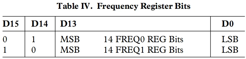
In the control word, D15 and D14 are used to specify the frequency register to be written to:
- D15 = 0, D14 = 1: Write to the FREQ0 register to select and modify the 14 MSB data bits
- D15 = 1, D14 = 0: Write to the FREQ1 register to select and modify the 14 LSB data bits
2. Writing to the Phase Register
The phase register determines the phase offset of the output signal, and its calculation formula is as follows:
Wherein, PHASEREG is the value in the selected phase register, and the phase of the output signal will be shifted accordingly.
The phase register is 12 bits wide. When writing, both D15 and D14 of the control word must be set to 1. The D13 bit determines the phase register to be written:
- D13 = 0: Write to the PHASE0 register
- D13 = 1: Write to the PHASE1 register
1.4.4.3 AD9833 Sleep Function and Low-Power Register
The sleep function (SLEEP Function) of the AD9833 chip can turn off part or all of the internal clock and DAC by setting specific bits in the control register to minimize power consumption. The sleep function can be configured via the two control bits SLEEP1 and SLEEP12, whose combination determines which parts of the chip will be turned off or remain active.
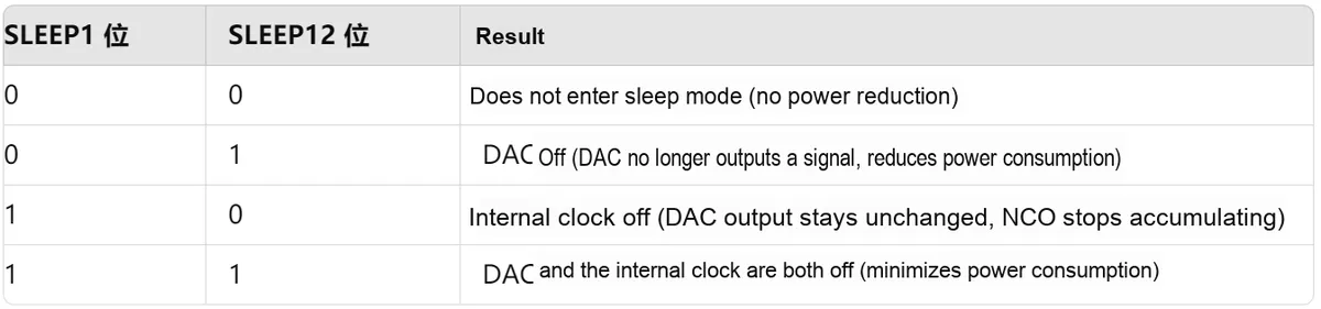
When the DAC is disabled (SLEEP1 = 0, SLEEP12 = 1), the internal DAC of the AD9833 is powered down, and this mode is suitable for scenarios where only the most significant bit (MSB) of the DAC output data needs to be output.
When the internal clock is to be disabled (SLEEP1 = 1, SLEEP12 = 0), the NCO (Numerically Controlled Oscillator) stops phase accumulation, and the DAC output will remain at the current value. However, new frequency, phase and control words can still be written to the registers at this point, and the selected frequency and phase registers can also be changed via control bits. After the SLEEP1 bit is reset to 0, the MCLK (Master Clock) will be re-enabled, and the previous changes to the registers will be reflected in the output after a certain delay.
1.4.4.4 AD9833 Output Mode
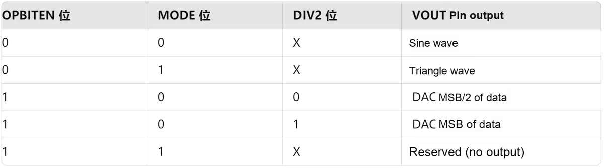
The output pin (VOUT) of the AD9833 can provide multiple types of signal outputs, including the most significant bit (MSB) of DAC data, sine wave output or triangular wave output; the selection of these output modes is determined by the OPBITEN (bit D5), MODE (bit D1) and DIV2 (bit D3) in the control register.
When using the AD9833 to output waveforms, the following two points should be noted:
- Output waveform amplitude: When outputting sine waves and triangular waves, the waveform amplitude ranges from 38 mV to 650 mV; when outputting square waves, the maximum amplitude is 3.3 V. If sine waves and triangular waves with larger amplitude are required, an operational amplifier is needed to boost the amplitude, and a digital potentiometer can be added to the amplifier circuit to adjust the amplitude.
- Output waveform frequency: The maximum output waveform frequency of the AD9833 can reach 12.5 MHz, and this value is related to the Nyquist Sampling Theorem. The maximum input clock frequency of the AD9833 is 25 MHz. According to the Nyquist Sampling Theorem, to accurately reconstruct a signal, the sampling frequency must be twice the highest frequency of the signal; in other words, at least 2 sampling points are required in each cycle of the output waveform. Therefore, the maximum output frequency is half of the input clock frequency, which is 12.5 MHz.When we add a digital potentiometer to an amplifier circuit to adjust the amplitude, special attention should be paid to the bandwidth of the digital potentiometer, which determines its response capability to signals at different frequencies. When the frequency of the output signal is relatively high, if the bandwidth of the digital potentiometer is insufficient, the high-frequency components of the signal will be suppressed, resulting in a significant reduction in the amplitude of the waveform. Common digital potentiometers such as AD5260, X9C103, and AD5292 all have a bandwidth of around 1 MHz.If you need to process signals up to 10 MHz, you can use a high-frequency variable gain amplifier (VGA), such as the AD8367. This is a high-frequency amplifier with integrated gain control, featuring a bandwidth of up to 500 MHz, and it can replace traditional digital potentiometers for signal amplitude adjustment.
1. Square wave output / Most Significant Bit (MSB) of DAC data
When the OPBITEN bit (bit D5) in the control register is set to 1, the most significant bit (MSB) of the DAC data will be output to the VOUT pin. This output is typically used as a coarse clock source, since the MSB outputs a square wave signal. Users can also use the DIV2 bit (bit D3) in the control register to determine whether the frequency of this square wave signal needs to be divided by two before output.
2. Sine Wave Output
The SIN ROM module of the AD9833 converts the phase information from the frequency register and phase register into amplitude information, thereby outputting a sine wave signal at the VOUT pin. To output a sine wave signal at the VOUT pin, it is necessary to set the MODE bit (bit D1) in the control register to 0, and simultaneously set the OPBITEN bit (bit D5) to 0.
3. Triangular Wave Output
To achieve triangular wave output, the MODE bit (bit D1) in the control register needs to be set to 1. In this case, the SIN ROM module is bypassed, and the truncated digital output of the NCO (Numerically Controlled Oscillator) is directly sent to the DAC. At this point, the output of the VOUT pin is no longer a sine wave, but a 10-bit linear triangular wave signal.
It should be noted that no matter which output mode is selected, the SLEEP12 bit (which controls the power state of the DAC) must be set to 0 to ensure that the DAC is enabled so that the signal can be correctly output to the VOUT pin.
1.5 Introduction to Digital Potentiometer Chips
As we mentioned earlier, when the AD9833 chip outputs sine waves and triangular waves, the waveform amplitude ranges from 38 mV to 650 mV. If we require sine waves and triangular waves with a larger amplitude, we need to use an operational amplifier to boost the amplitude. Common operational amplifier circuits include two types: non-inverting amplifier circuits and inverting amplifier circuits, as shown in the figure below:
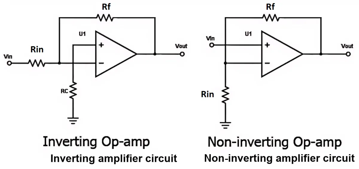
Wherein, the amplification factor of the non-inverting amplifier circuit is, and the amplification factor of the inverting amplifier circuit is, in whichis the feedback resistor, andis the input resistor. The output signal of the non-inverting amplifier circuit is in phase with the input signal; it features high input impedance and low output impedance, and can be directly connected to a high-impedance signal source. The output signal of the inverting amplifier circuit is 180 degrees out of phase with the input signal; its input impedance is determined by the input resistor, and it has low output impedance, making it suitable for low-impedance loads.
If we want to adjust the gain of an operational amplifier circuit, we can usually replace the feedback resistor () with a potentiometer (variable resistor); this method is simple and intuitive, and enables gain adjustment:
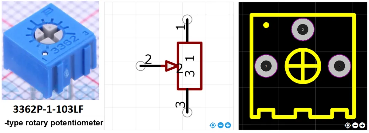
However, there are also certain drawbacks to adjusting the gain of an amplifier circuit via a potentiometer:
- Influence of Mechanical Vibration on Adjustment: potentiometers are mechanical components that are susceptible to mechanical vibration, which may result in unstable gain or gain drift.
- Low positioning accuracy: The gain adjustment accuracy of the potentiometer is limited. Especially when fine adjustment is required in high-precision signal conditioning circuits, the markings on the are not precise enough, which is prone to errors.
- Not easy to adjust automatically: potentiometers usually require manual adjustment, making them unsuitable for automated control or program-controlled tuning.
- Wear after prolonged use: potentiometers are mechanical components. Over time and with extended use, their performance may degrade due to friction and wear, resulting in unsmooth adjustment or even complete failure.
In this case, we can use a digital potentiometer instead of a potentiometer to adjust the signal amplitude. Compared with the potentiometer configured on the operational amplifier, the digital potentiometer has the following advantages:
- High positioning accuracy: Digital potentiometers use digital signals to precisely control the adjustment of resistance, which means that each step of adjustment can accurately reach the preset value, featuring extremely high accuracy.
- Immune to mechanical vibration: Digital potentiometers have no mechanical components and rely on digital signals for control, so they are not affected by external mechanical vibration, shock, or wear caused by prolonged use, delivering better stability.
- Program-controlled adjustment, suitable for automation: Digital potentiometers can be controlled by devices such as microcontrollers and computers, making them ideal for scenarios including automated systems, semi-automated adjustment, and remote control.
In addition, we can also use a digital potentiometer to simulate the function of a DAC. In low-frequency signal generation circuits, a digital potentiometer can be used to adjust the waveform amplitude so as to generate simple analog signals.
In the following content, we discuss digital potentiometer chips with two types of communication interfaces:
- MCP41010: It adopts the SPI interface and requires 3 communication lines (SCK, MOSI, CS). This digital potentiometer chip is suitable for use in conjunction with the AD9833 chip to realize output voltage amplitude adjustment, and the reasons for its selection are as follows:
- The AD9833 itself is configured via SPI (the default interface of the AD9833 is SPI), and the MCP41010 can share the same SPI bus with the AD9833, requiring only one additional chip select (CS) pin to be allocated, which saves GPIO resources.
- The MCP41010 features a high-speed SPI communication interface (typical value: 10MHz), which enables rapid updates of the resistance value for a faster response.
- The MCP41010 is a digital potentiometer with 8-bit resolution (256 levels), featuring finer adjustment steps and being suitable for scenarios requiring high-precision amplitude control.
- DS3502: Adopts the I2C interface and requires 2 communication lines (SDA, SCL). This digital potentiometer chip is suitable for scenarios where multiple I2C devices need to be connected and the requirements for resolution are not high:
- The DS3502 chip features 7-bit resolution, which can meet basic voltage/current regulation requirements, such as dimming for LED lighting.
- The DS3502 shares the bus via I2C addresses (supporting 4 optional addresses). Meanwhile, the I2C bus features extremely low power consumption when idle, making it suitable for applications requiring multiple potentiometers to work in coordination (such as audio multi-channel equalizers) or for use in portable devices.
You can make your choice based on your specific application scenarios.
1.5.1 DS3502 Digital Potentiometer Chip
1.5.1.1 Introduction to Digital Potentiometer DS3502
The DS3502 is a 7-bit digital potentiometer, which can be communicated with and have its resistance adjusted via an I2C interface by a microcontroller. The DS3502 provides 128 resistance adjustment steps, and this device supports a wide range of supply voltages, typically operating between 2.7 V and 5.5 V.
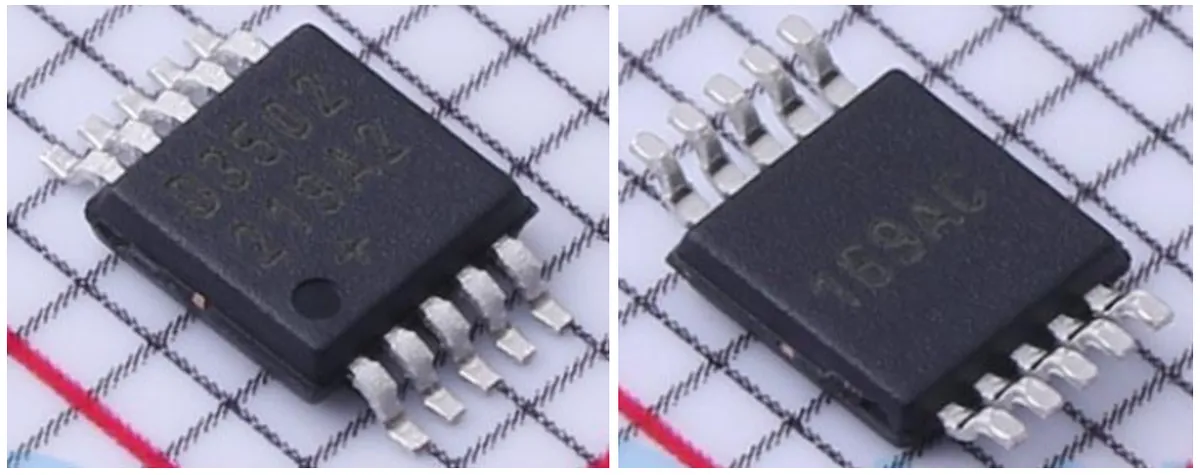
The DS3502 can operate at speeds up to 400kHz, with a maximum resistance value of 10kΩ. By adjusting the two address setting pins, up to four DS3502 digital potentiometers can be supported on the same bus. It also features an EEPROM function that can store the set 7-bit resistance value after power-off.
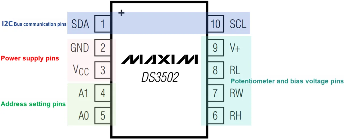
The pins and functions of the DS3502 are as follows:
Pin Name | Pin Number | Pin Functions |
SDA | 1 | I2C Serial Data: Used for the input and output of I2C data. The voltage of SDA ranges from -0.5V to (VCC + 0.5V), and shall not exceed + 6.0V. |
SCL | 10 | I2C Serial Clock: The input pin of the I2C clock, which is responsible for synchronizing data transmission. The voltage of SCL ranges from -0.5V to (VCC + 0.5V), and shall not exceed + 6.0V. |
VCC | 3 | Power supply voltage terminal: Connects to an external power source to provide the operating voltage required for the device, which typically ranges from 2.5V to 5.5V. |
GND | 2 | Ground terminal: the grounding terminal of a device, which serves as the reference point for the circuit. |
A1, A0 | 4, 5 | Address selection input: Used to determine the I2C slave address. |
RH | 6 | High-end terminal: the high end of the potentiometer, which is connected to the positive power supply in the application. The voltage range is from -0.5V to V+. |
RW | 7 | Slider terminal: The sliding end of a potentiometer, which outputs an adjustable voltage and is usually connected to a load or a subsequent circuit. The voltage range is from -0.5V to V+. |
RL | 8 | Low-end terminal: the low end of a potentiometer, connected to ground or a negative power supply. The voltage range is from -0.5V to V+. |
V+ | 9 | Slide Bias Voltage: Provides a bias voltage for the sliding terminal, with a voltage range from -0.5V to + 17V, which affects the output voltage range. |
1.5.1.2 Internal Structure and Working Principle of the DS3502 Chip
The internal structure of the DS3502 chip is shown as follows, whose core units include an I2C communication interface, control registers, a sliding register and a resistor network:
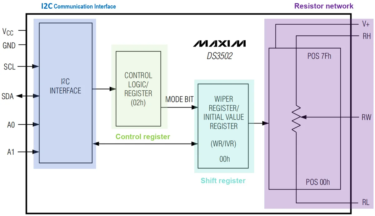
The wiper position of the DS3502 is controlled by the value in the Wiper Register (WR). Upon power-up, the initial value of the wiper position is programmed via the Initial Value Register (IVR); after power-up, the data in the IVR is loaded into the WR to set the initial position of the potentiometer's wiper terminal (RW).

The Control Register (CR) is located at address 02h and contains the WR/IVR address mode bit (MODE bit), which determines how the WR and IVR data registers are written via I2C:
- MODE = 0: When writing to address 00h via I2C, data will be written to WR and IVR (CR = 00h); when reading from address 00h via I2C, the content of WR will be returned. This mode is relatively slow as it involves writing to EEPROM registers.
- MODE = 1: When writing to address 00h via I2C, only the WR register (CR = 80h) is written; when reading from slave address 00h via I2C, the content of WR is still returned. This mode enables fast writing to SRAM without waiting for the write delay associated with EEPROM registers.
The data in EEPROM and SRAM remains unchanged when the MODE bit is switched, and the default value of the CR control register is 00h upon power-on.
The potentiometer of the DS3502 consists of 127 series resistors connected between the RH and RL pins. By changing the value (a decimal value ranging from 0 to 127) in the Wiper Register (WR), the internal decoder of the DS3502 controls the corresponding MOS transistors to turn on or off. These MOS transistors act as switches in the resistor network to select which resistor node the wiper terminal (RW) is connected to: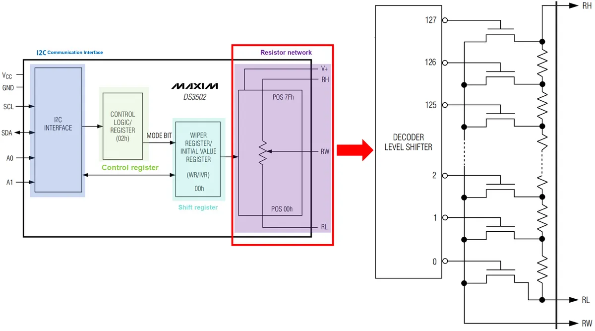
- MOSFET turn-on: When a control signal turns on a certain MOSFET, the resistor segment corresponding to that MOSFET is incorporated into the circuit
- MOSFET turn-off: When the MOSFET is turned off, the corresponding node is disconnected from the sliding terminal RW, so that no current can flow through this path, and RW is independent of this resistor segment.
Based on this principle, we can adjust the resistance value of the wiper terminal of the DS3502 to achieve different voltage outputs. If RH, RL and RW are connected in a voltage divider configuration, the voltage across RW can be calculated using the following formula:
Wherein,is the wiper position, expressed in decimal (0-127),is the voltage at the RL terminal,and is the voltage at the RH terminal.
Here, in the DS3502 chip's datasheet under the electrical characteristics section, we can see that after the wiper is adjusted to a new resistance value, it takes 1μs (i. e., the wiper response time tWRS) to stabilize:
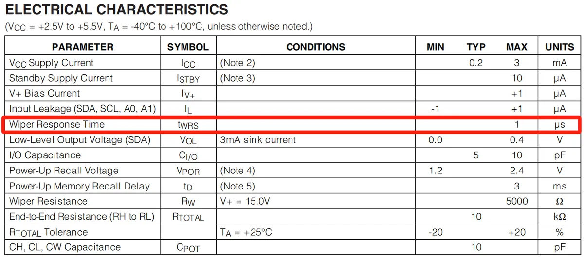
Therefore, theoretically, when the DS3502 acts as a variable voltage divider to adjust the output voltage, its maximum operating frequency is 1 MHz (1/tWRS).
1.5.1.3 Communication Protocol of the DS3502 Chip
The I2C communication address of the DS3502 chip is determined by the two pins A1 and A0:
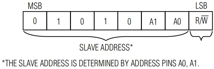
When writing single-byte data to the DS3502 chip using a microcontroller, it is necessary to write the device address (both A0 and A1 in the diagram below are connected to GND), the register address and the data to be written, as shown below:

For example, when writing to the WR register, the communication process is as follows:

When the CR register MODE bit is set to 0, since writing to the EEPROM register takes a certain amount of time, the master device can determine whether the DS3502 has completed the EEPROM register write operation by repeatedly addressing the DS3502 to check for a response; alternatively, the master can directly wait for the maximum EEPROM write time (tW), which is specified as 20ms in the Electrical Characteristics section of the DS3502 datasheet:

When reading single-byte data from the DS3502 chip using a microcontroller, take reading the value of the CR control register as an example:
- First, send the slave address byte, set the R/W bit to 0 to perform a dummy write operation, and the slave will send an ACK response signal.
- Write the memory address 02h to be read, and the slave sends an ACK response signal
- Generate repeated START conditions to maintain communication
- Write the slave address again and set the R/W bit to 1, indicating that data reading is to be performed.
- The slave device transmits single-byte data of the corresponding register, the master device reads the data byte, uses a NACK signal to indicate the end of transmission, and generates a STOP condition.
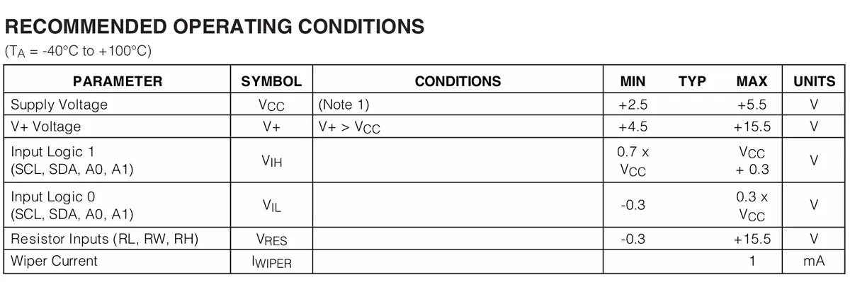
When using the DS3502 chip, it should be noted that 0.01µF and 0.1µF capacitors are required for decoupling at the power supply pin (VCC) and the wiper voltage pin (V+), and 4.7kΩ pull-up resistors shall be used for the SDA and SCL pins;additionally, if the voltage of RH is higher than VCC, the voltage of V+ must be the same as or higher than that of RH, which means V+ needs to be connected to RH.
At the same time, it should be noted that the voltage range of the sliding voltage pin (V+) is + 4.5V to 15.5V:
1.5.2 MCP41010 Digital Potentiometer Chip
1.5.2.1 Introduction to Digital Potentiometer MCP41010
The MCP41010 is a single-channel, 8-bit resolution digital potentiometer available in 10 kΩ, 50 kΩ and 100 kΩ resistance variants, and is controlled via an SPI interface:
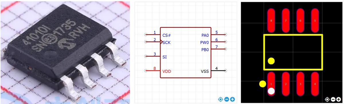
Its main features include:
- 256-step adjustment: Each potentiometer features 256 adjustable positions to deliver precise resistance regulation
- High Precision: Features maximum integral nonlinearity and differential nonlinearity of ±1 LSB (Least Significant Bit), ensuring precise resistance control
- Low Power Consumption: The MCP41010 adopts low-power CMOS technology, with a maximum current consumption of only 1 µA during static operation, making it suitable for low-power applications.
- Single-supply operation: supports an operating voltage range of 2.7V to 5.5V
- Power-off Function: Built-in software-controlled power-off function, which can disconnect all resistive circuits to minimize power consumption.
- Mid-position reset: When powered on, the MCP41010 chip resets its wiper to the mid-position (80h) to ensure a consistent initial state.
The MCP41010 chip is provided with 8 pins, and the main pins include: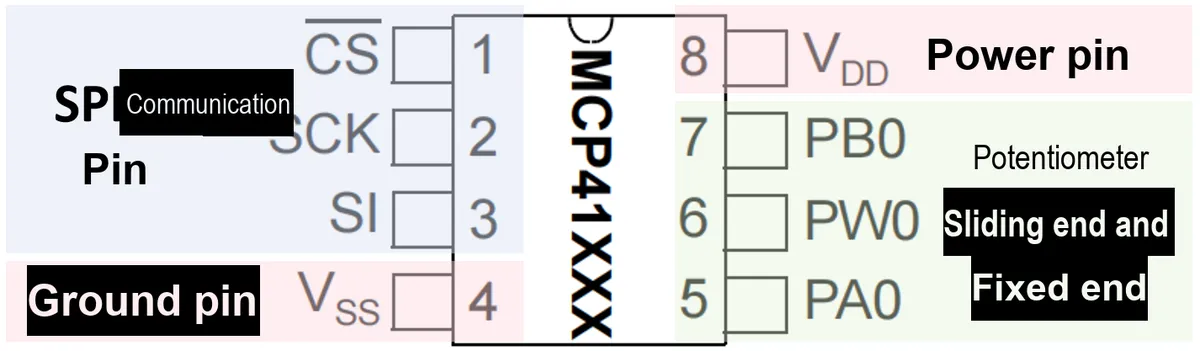
- Chip Select Pin CS: This is the chip select pin of the SPI interface, which is used to select the current device for communication. When the CS pin is at low level, the SPI interface is activated and starts receiving data; after the data is loaded into the shift register, CS switches from low level to high level, and the command takes effect.
- Clock Pin SCK: The clock pin of the SPI interface, which is used to synchronize data transmission; data is written via SI (Serial Data Input pin) on the rising edge of SCK
- Data Input Pin SI: the serial data input pin of the SPI interface, used for inputting commands and data
- Power supply pin VDD: the positive power input terminal of the chip, with an operating voltage range from 2.7V to 5.5V
- Ground Pin VSS: The ground pin of the chip, used as the negative terminal connection of the power supply
- Fixed terminals PA0 and PB0: These are the fixed terminal A of potentiometer 0; terminals A and B are connected to both ends of the resistor array, and the wiper terminal (PW0) moves between A and B. Depending on the wiper position, the resistance between A and PW can be adjusted within the range from 0Ω to the full resistance value.
- Wiper Output PW0: This is the wiper output terminal of the potentiometer. PW0 serves as the intermediate node of the resistor network; the resistance distribution of PW0 between terminal A and terminal B can be adjusted via control commands, and the output voltage or resistance is provided through this pin.
1.5.2.2 Internal Structure and Working Principle of MCP41010 Chip
The internal structure of the MCP41010 chip includes a power input terminal, control logic, a 16-bit shift register, a resistor array, a tap control register, and SPI interface pins:
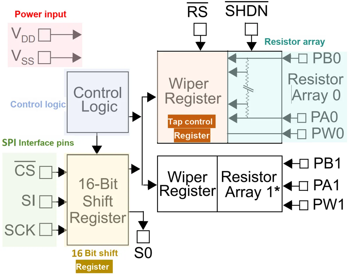
The functions of each constituent unit are as follows:
- Power Input Terminals (VDD and VSS): supply the operating voltage, support single-power supply, with an operating voltage range from 2.7V to 5.5V; the supply voltage and current are specified in the datasheet.

- Control Logic: The control logic module is configured to interpret commands and data transmitted via the SPI interface, and this module updates the internal tap control register according to the input commands and data.
- 16-bit shift register: It receives external input data and commands via the SPI interface, shifts data in accordance with the clock signal (SCK), and after receiving 16-bit data, decodes the command through the control logic module and adjusts the position of the sliding contact of the resistor network.
- Resistor array: A resistor array consists of a fixed resistor network with a total of 256 taps (or steps), and the resistance value of each tap is equal.
- Tap Control Register: stores the position data (8-bit, ranging from 0x00 to 0xFF) of the current tap (sliding contact). The sliding contact divides the resistor array into two parts: terminals PA and PB correspond to different resistance values, and PW is the tap output terminal.
Simply put, the MCP41010 chip primarily achieves resistance value adjustment or voltage division function through a resistor array:
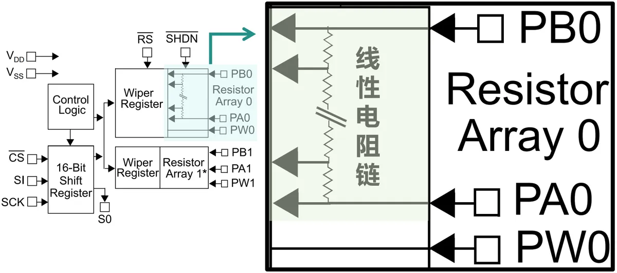
A resistor array consists of a series of fixed resistor units (e. g., 100Ω or 1kΩ; for the MCP41010 chip, the total resistance of its resistor array is 10kΩ, and a single resistor unit is 52Ω) connected end to end to form a linear resistor chain, with the two ends of the resistor chain connected to the PA and PB pins respectively.When we use an MCU to send the resistance value to be adjusted to the MCP41010 chip via the SPI interface, the control logic module of the MCP41010 chip updates the value stored in the internal tap control register (8-bit data, ranging from 0x00 to 0xFF, used to determine the position of the wiper) according to the input commands and data. Each digital value (0~255) corresponds to a node in the resistor network, and the sliding contact PW pin can switch between the nodes on the resistor chain, thereby changing the resistance value between A and W or between W and B.
1.5.2.3 Communication Protocol of the MCP41010 Chip
Next, we will explain the SPI Communication Protocol of the MCP41010 chip. When operating the MCP41010 chip, it is necessary to use the SPI interface of the MCU to send 16-bit data each time: the first 8 bits are the command byte, and the last 8 bits are the data byte. Data transmission starts by setting the CS (chip select pin) to a low level, all data is written on the rising edge of SCK (clock pin), and the SCK (clock pin) remains at a low level when idle;After the 16-bit data is transmitted completely, pull the CS (chip select pin) high, and the MCP41010 chip will write the data byte into the tap control register and clear the 16-bit shift register:
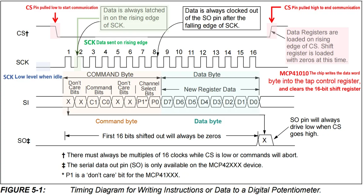
The command byte (the first 8 bits) consists of command select bits (C1, C0, bits 4:5), potentiometer select bits (P1, P0, bits 0:1) and don't-care bits, where the logic level of the don't-care bits has no impact on the command:
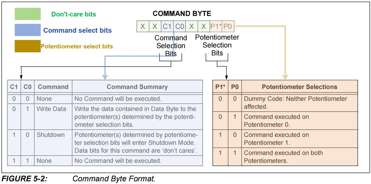
The meanings of the command select bits (C1, C0, bits 4:5) are as follows:
- When C1 and C0 are 00 or 11: no command is executed
- When C1 and C0 are 01: Write the data in the data byte to the potentiometer specified by the potentiometer selection bit
- When C1 and C0 are 10: the potentiometer specified by the potentiometer selection bits will enter the power-down mode, and the data bits of this command are "don't care" bits.
For the MCP41010 chip, which is a single-channel digital potentiometer, the potentiometer select bits (P1, P0, bits 0 and 1) are always 01; the data byte (the last 8 bits) is used to set the new value of the potentiometer, which ranges from 0 to 255.
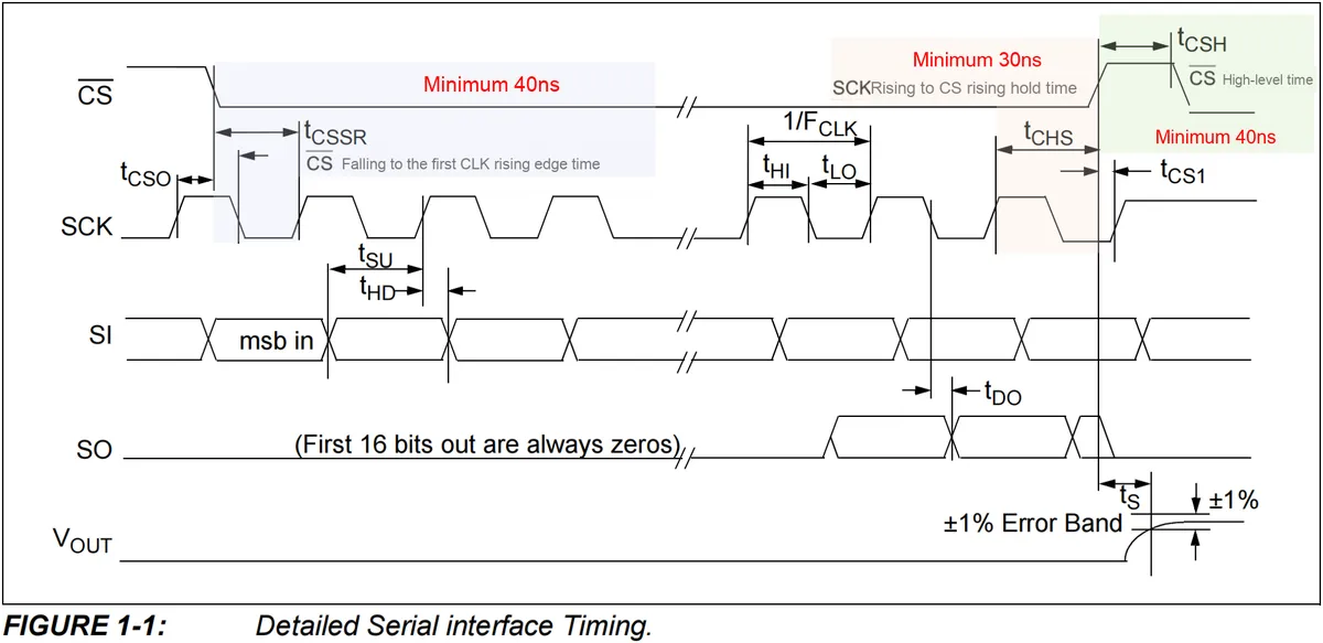
The SPI communication electrical specifications of the MCP41010 chip are as follows:
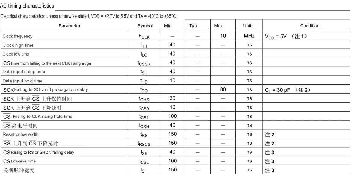
Its maximum clock frequency is 10MHz, and the other key parameters are marked in the following figure:
1.5.2.4 Operating Modes and Application Examples of the MCP41010 Chip
The operating modes of the MCP41010 chip can be divided into the following two types: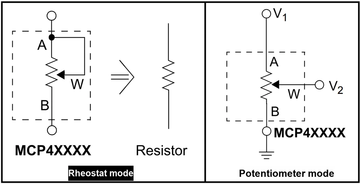
- Rheostat Mode: In rheostat mode, the MCP41010 functions as a two-terminal variable resistor, with the chip’s terminal A and terminal W short-circuited, and terminal B connected to the other end of the circuit; by adjusting the position of the wiper, the resistance between terminal A/W and terminal B can be varied, with the minimum value being
00h(the minimum resistance value, approximately 52Ω) and the maximum value beingFFh(close to the total resistance value); the step size (LSB) per adjustment is 1/256 of the total resistance. It should be noted that the wiper current must be controlled within 1mA to avoid damaging the internal circuitry. - Potentiometer Mode: In potentiometer mode, all three terminals (A, B, W) of the MCP41010 are connected to the circuit to form a voltage divider. Terminals A and B are connected to the power supply or signal input, and terminal W outputs the divided voltage. By adjusting the position of the wiper, the voltage value output from terminal W can be changed. The output voltage at terminal Wis, whereandare the input voltages at terminals A and B,andare the resistance values on either side of the wiper,and is the total resistance (i. e., the resistance between terminals A and B)
The following is a circuit with adjustable amplification factor based on the MCP41010 digital potentiometer and MCP606 operational amplifier:
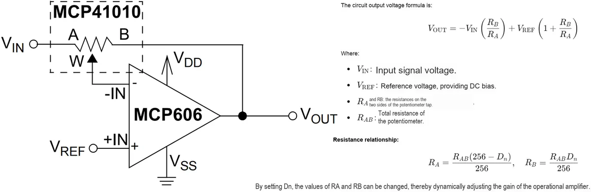
Among them, the MCP606 operates in an inverting amplifier configuration, and we can set the voltage division ratio of the potentiometer by adjusting the position of the adjustable output W, thereby changing the gain of the inverting amplifier.
As we mentioned earlier, the total resistance of the resistor array of the MCP41010 chip is 10kΩ, which consists of multiple 52Ω resistor units (with a resolution of 52Ω per step). When we need to achieve fine adjustment of the voltage divider, two MCP41010 digital potentiometers can be used in combination, one for coarse adjustment and the other for fine adjustment, so as to improve the precision and flexibility of the adjustment:
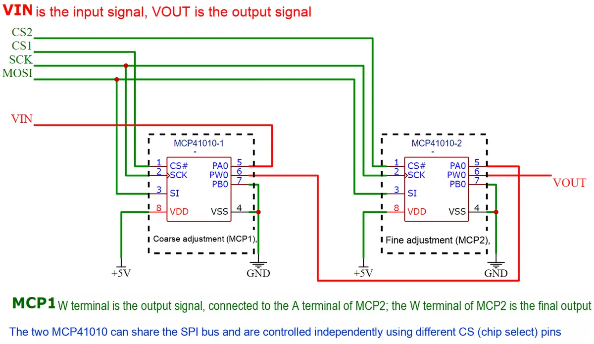
As shown in the figure above, the coarse adjustment (MCP1) is used to control the main resistance range of the potentiometer, while the fine adjustment (MCP2) serves for fine-tuning the resistance value. The W terminal of MCP1 acts as the output signal, which is connected to the A terminal of MCP2; the W terminal of MCP2 functions as the final output terminal. In addition, the B terminals of both MCP1 and MCP2 are grounded, and their A terminals are connected to the signal input. The two MCP41010 chips share the same SPI bus, and are independently controlled via their respective CS (chip select) pins.
After connecting in this manner, if you need to adjust the resistance to the range of 0 to 10 kΩ, you can set the coarse adjustment MCP1 to perform a wide-range adjustment of 0 to 9 kΩ, while the fine adjustment MCP2 is used for fine-tuning within the small range of 0 to 1 kΩ.
1.5.2.5 Precautions for the Use of the MCP41010 Chip
It should be noted here that the MCP41010 is a digital potentiometer based on a resistor network, and its internal distributed capacitance and parasitic inductance will limit the frequency range it can support. According to official data and actual tests, the signal gain of the MCP41010 will attenuate significantly above 1 MHz, resulting in a reduction in the amplitude of the output waveform and even distortion.
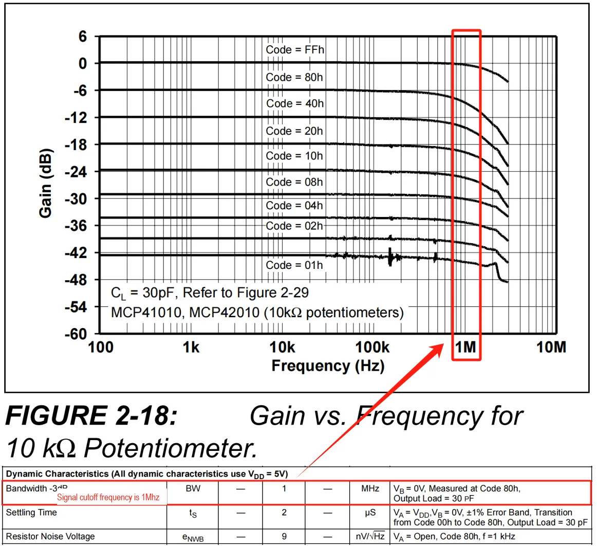
If we need to use a digital potentiometer to adjust the amplitude of high-frequency signals in an operational amplifier circuit, we can adopt a digital potentiometer specifically designed for high-frequency signals, such as the AD5292 or MAX5481 chips, which feature higher bandwidth and superior high-frequency performance; alternatively, a programmable gain amplifier (PGA) can be used as a replacement.
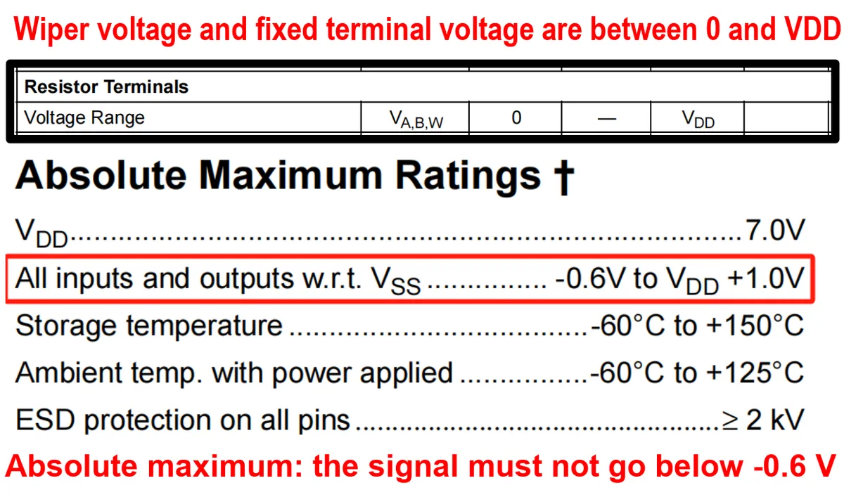
Meanwhile, it should be noted here that since the MCP41010 is a single-supply powered chip (typical supply voltage range is 2.7V ~ 5.5V, corresponding to VDD in the datasheet), this means its Scope of Work is limited between 0V and VDD. If the input signal is lower than 0V (i. e., a negative voltage, for example, when the input signal is a sine wave with a center level of 0V), signal distortion will occur in the MCP41010.
2. Software Control Method
2.1 Custom Class for MCP4725
Here, we have customized a driver class for the MCP4725 chip, and the sample code is as follows:
# Python env   : MicroPython v1.23.0
# -*- coding: utf-8 -*-
# @Time    : 2024/9/1 2:10 PM
# @Author  : Li Qingshui
# @File    : mcp4725.py
# @Description : Driver module for the 12-bit DAC chip MCP4725
# Reference code: https://github.com/wayoda/micropython-mcp4725/blob/master/mcp4725.py

# ======================================== Import Modules =========================================

# Import hardware-related modules
from machine import I2C

# ======================================== Global Variables ============================================

# ======================================== Functions ============================================

# ======================================== Custom Classes ============================================

# Custom class for the MCP4725 DAC chip
class MCP4725:
    """
    The MCP4725 class controls the MCP4725 digital-to-analog converter (DAC) chip, communicating with the main controller chip over the I2C interface to output analog voltage values.

    Attributes:
        i2c (machine.I2C): I2C interface object used to communicate with the MCP4725.
        address (int): I2C address of the MCP4725. Defaults to 0x60.
        _writeBuffer (bytearray): Buffer that stores the data to be written to the DAC.

    Class Variables:
        BUS_ADDRESS (list): Possible I2C addresses of the MCP4725. Defaults to [0x60, 0x61, 0x62, 0x63, 0x64, 0x65, 0x66, 0x67].
        POWER_DOWN_MODE (dict): Power-down mode mapping dictionary, containing the four modes 'Off', '1k', '100k', and '500k'.

    Methods:
        __init__(i2c: machine.I2C, address: int = 0x60):
            Initializes the MCP4725 instance and sets the I2C communication object and address.

        write(value: int) -> bool:
            Writes an analog value to the MCP4725, with the value ranging from 0 to 4095, and returns whether the write succeeded.

        read() -> tuple:
            Reads status information from the MCP4725, including the power-down mode, DAC output value, and so on.

        config(power_down: str = 'Off', value: int = 0, eeprom: bool = False) -> bool:
            Configures the power-down mode and output value of the MCP4725, with an option to write to the EEPROM.

        _powerDownKey(value: int) -> str:
            Converts the power-down mode code to the mode name, for use in configuration and read operations.
    """

    # Class variables
    # Define the I2C address of the MCP4725; generally 0x60 or 0x61 can be chosen
    BUS_ADDRESS = [0x60, 0x61, 0x62, 0x63, 0x64, 0x65, 0x66, 0x67]
    # Define the power-down modes of the MCP4725; the keys are mode names and the values are mode codes
    POWER_DOWN_MODE = {'Off': 0, '1k': 1, '100k': 2, '500k': 3}

    def __init__(self, i2c: I2C, address: int = 0x60) -> None:
        """
        Initializes the MCP4725 chip.

        This method initializes the basic settings of the MCP4725 DAC chip, including the I2C communication object and the I2C address.

        Args:
            i2c (I2C): I2C object used to communicate with the MCP4725 chip.
            address (int, optional): I2C address of the MCP4725. Defaults to 0x62.

        Returns:
            None: This method has no return value.

        Raises:
            ValueError: Raised if the address passed in is not within the valid I2C address range.
        """

        if address not in self.BUS_ADDRESS:
            raise ValueError(f"Invalid I2C address: {hex(address)}. Valid addresses are: {self.BUS_ADDRESS}")

        # Initialize the I2C communication and address of the MCP4725
        self.i2c = i2c
        self.address = address
        # Buffer used to store the value written to the DAC
        self._writeBuffer = bytearray(2)

    def write(self, value: int) -> bool:
        """
        Writes an analog value to the MCP4725 DAC and outputs it.

        This method converts the input analog value into a format the DAC can recognize and writes it to the MCP4725 DAC chip over the I2C interface.

        Args:
            value (int): Analog value to output, ranging from 0 to 4095.

        Returns:
            bool: Returns True if the data was written successfully and 2 ACKs (acknowledgements) were received; otherwise returns False.

        Raises:
            ValueError: Raised if the `value` passed in is not within the range 0 to 4095.
        """
        if not (0 <= value <= 4095):
            raise ValueError("Value must be between 0 and 4095")

        # Limit the input value to between 0 and 4095 and make sure it is 12 bits
        value = value & 0xFFF

        # Store the high 8 bits in the first byte of the buffer
        self._writeBuffer[0] = (value >> 8) & 0xFF
        # Store the low 8 bits in the second byte of the buffer
        self._writeBuffer[1] = value & 0xFF

        # Write the buffer contents to the DAC and return the number of ACKs received from the slave
        return self.i2c.writeto(self.address, self._writeBuffer) == 2

    def read(self) -> tuple:
        '''
        Reads the power-down data bits and DAC data bits from the MCP4725 chip.

        This method reads 5 bytes of data from the MCP4725 chip and parses out the power-down status, the DAC output value, and the data in the EEPROM.

        The returned data includes:
        - Whether an EEPROM write is in progress
        - The current power-down mode
        - The current DAC output value
        - The power-down mode stored in EEPROM
        - The DAC output value stored in EEPROM

        Returns:
            tuple: If the read succeeds, returns a tuple containing the following information:
                - eeprom_write_busy (bool): Whether an EEPROM write is in progress. True means not busy, False means busy.
                - power_down (str): The current power-down mode (such as "normal operation" or "power-down").
                - value (int): The current DAC output value, in the range 0 to 4095.
                - eeprom_power_down (str): The power-down mode stored in EEPROM.
                - eeprom_value (int): The DAC output value stored in EEPROM, in the range 0 to 4095.

            If the read fails or the data length is incorrect, returns None.

        Raises:
            None: This method does not raise exceptions.
        '''
        # Create a buffer for receiving data
        buf = bytearray(5)
        # Read 5 bytes of data from the MCP4725 into the buffer
        self.i2c.readfrom_into(self.address, buf)
        # Check whether the buffer length is 5
        if len(buf) == 5:
            # Read the EEPROM write busy status
            eeprom_write_busy = (buf[0] & 0x80) == 0
            # Read the current power-down mode
            power_down = self._powerDownKey((buf[0] >> 1) & 0x03)
            # Read the current output value
            value = ((buf[1] << 8) | (buf[2])) >> 4
            # Read the power-down mode stored in EEPROM
            eeprom_power_down = self._powerDownKey((buf[3] >> 5) & 0x03)
            # Read the output value stored in EEPROM
            eeprom_value = ((buf[3] & 0x0f) << 8) | buf[4]
            # Return a tuple containing all the data read
            return (eeprom_write_busy, power_down, value, eeprom_power_down, eeprom_value)
        return None

    def config(self, power_down: str = 'Off', value: int = 0, eeprom: bool = False) -> bool:
        """
        Configure the power-down mode and output value of the MCP4725 chip.

        This method configures the power-down mode and voltage output value of the MCP4725 chip, and whether to write the configuration to EEPROM.

        Args:
            power_down (str, optional): Power-down mode, default 'Off'; options include 'Mode1', 'Mode2', 'Mode3', etc. See MCP4725.POWER_DOWN_MODE for the exact values.
            value (int, optional): The analog value to output, in the range 0 to 4095, default 0.
            eeprom (bool, optional): Whether to write the configuration to EEPROM, default False.

        Returns:
            bool: Returns True if the write succeeds, otherwise False.

        Raises:
            ValueError: If the power-down mode is invalid, the analog value is out of range, or the `eeprom` parameter has the wrong type.
        """
        # Check whether the input power-down mode is valid
        if power_down not in MCP4725.POWER_DOWN_MODE.keys():
            raise ValueError("Invalid power down mode: {}".format(power_down))

        # Check whether the analog value is between 0 and 4095
        if not (0 <= value <= 4095):
            raise ValueError("Value must be between 0 and 4095")

        # Check whether eeprom is a boolean
        if not isinstance(eeprom, bool):
            raise ValueError("eeprom must be a boolean value")

        # Initialize the buffer used for configuration
        buf = bytearray()
        # Set the configuration byte, including the power-down mode
        conf = 0x40 | (MCP4725.POWER_DOWN_MODE[power_down] << 1)

        if eeprom:
            # If writing to EEPROM is required, set the corresponding flag bit
            conf = conf | 0x60
        buf.append(conf)

        # Make sure the output value is within a reasonable range
        value = value & 0xFFF

        # Store the upper 8 bits of the output value in the buffer
        buf.append(value >> 4)
        # Store the lower 4 bits of the output value in the buffer
        buf.append((value & 0x0F) << 4)

        # Write the configuration buffer to the MCP4725 and return whether the write succeeded
        return self.i2c.writeto(self.address, buf) == 3

    def _powerDownKey(self, value: int) -> str:
        """
        Method that converts a power-down mode code to a mode name.

        This method looks up the mode name corresponding to the given power-down mode code.

        Args:
            value (int): Power-down mode code.

        Returns:
            str: The corresponding power-down mode name.

        Raises:
            KeyError: Raised if the code has no matching mode name.
        """
        for key, item in MCP4725.POWER_DOWN_MODE.items():
            if item == value:
                return key
        raise KeyError("No matching power down mode for value: {}".format(value))

# ======================================== Initialization ==========================================

# ========================================  Main Program  ===========================================
Simply put, we have done the following work:
Initialization method __init__(): Initialize the I2C communication and address of the MCP4725 in the constructor, and create a buffer for writing. Here, a two-byte contiguous memory region is created viabytearrayto pack the data into a ByteFlow for transmission.- Method for implementing the output value written to the DAC
write (): First, limit the input value to the range of 0 to 4095, then store the upper 8 bits and lower 8 bits into the_writeBufferbuffer respectively, and finally write the data in the buffer to the DAC via the I2C bus - Method for reading data from DAC
read (): Reads 5 bytes of data from the DAC, including the EEPROM write busy status, the current power-down mode and the power-down mode stored in EEPROM, the current output value and the output value stored in EEPROM, and finally returns the data in the form of a tuple. - Method for Implementing DAC Power-Down Mode Configuration
config (): Generates configuration bytes based on the input power-down mode and output value, supports optional writing of the configuration to EEPROM, and finally writes the configuration to the DAC via the I2C bus. - Implement an internal method
_powerDownKey (): which is used to convert the power-down mode code into the corresponding mode name.
Accordingly, we can use the following method to control the MCP4725 chip to generate the analog voltage output we require:
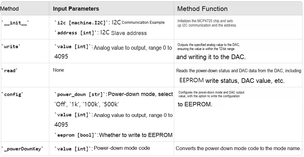
2.2 Custom Class of DS3502
In the following code, we implement the driver for the DS3502 digital potentiometer. We can control the position of the Wiper Register of the DS3502 via the I2C interface, so as to change the resistance value of the potentiometer.
The sample code is shown below:
# Python env   : MicroPython v1.23.0
# -*- coding: UTF-8 -*-
# @Time    : 2024/11/4 3:20 PM
# @Author  : Li Qingshui
# @File    : ds3502.py
# @Description : Driver module for the DS3502 digital potentiometer chip

# ======================================== Import Modules =========================================

# Import time-related modules
import time
# Import MicroPython-related modules
from micropython import const
# Import hardware-related modules
from machine import I2C

# ======================================== Global Variables ============================================

# ======================================== Functions ============================================

# ======================================== Custom Classes ============================================

# Custom class for the DS3502 digital potentiometer
class DS3502:
    """
    DS3502 class, used to operate the DS3502 digital potentiometer chip over the I2C bus to adjust the resistance value.
    This class wraps I2C communication with the DS3502 chip and provides functions such as setting the wiper register (WR) value, reading the current wiper position,
    and setting the control register (CR) mode.

    Attributes:
        i2c (I2C): I2C instance used to communicate with the DS3502.
        addr (int): I2C address of the DS3502 (between 0x28 and 0x2B).
        mode (int): Current operating mode (0 or 1), controlling write speed and non-volatile storage behavior.

    Methods:
        __init__(self, i2c: I2C, addr: int):
            Initialize a DS3502 class instance.
        write_wiper(self, value: int) -> None:
            Write the wiper register (WR) to set the wiper position.
        read_control_register(self) -> int:
            Read the value of the control register (CR) to determine the current write mode of the control register.
        set_mode(self, mode: int) -> None:
            Set the write mode of the control register.
        read_wiper(self) -> int:
            Read the value of the wiper register (WR).
    """

    # Define class variables: register addresses
    # WR wiper register address
    REG_WIPER = const(0x00)
    # CR control register address
    REG_CONTROL = const(0x02)

    def __init__(self, i2c: I2C, addr: int):
        """
        Initialize the DS3502 class.

        Args:
            i2c (machine.I2C): I2C object used to communicate with the DS3502.
            addr (int): I2C address of the DS3502 (between 0x28 and 0x2B).

        Raises:
            ValueError: If the address is not between 0x28 and 0x2B.
        """
        # Check whether the I2C address is between 0x28 and 0x2B
        if addr < 0x28 or addr > 0x2B:
            raise ValueError("Address must be between 0x28 and 0x2B")

        # Save the I2C object
        self.i2c = i2c
        # Save the I2C address
        self.addr = addr
        # Operating mode:
        #   0 - Write data to WR and IVR, slow, CR = 00h
        #   1 - Write data to WR only, fast, CR = 80h
        self.mode = 0

    def write_wiper(self, value: int) -> None:
        """
        Write the wiper register (WR) to set the wiper position.

        Args:
            value (int): Wiper register value to write (0 to 127).

        Raises:
            ValueError: If the value is not between 0 and 127.
        """

        # Check whether the input value is within the valid range
        if value < 0 or value > 127:
            raise ValueError("Value must be between 0 and 127")

        # Write the value to address 0x00 of the DS3502 to update the WR register
        self.i2c.writeto_mem(self.addr, DS3502.REG_WIPER, bytes([value]))

        # Decide whether a delay is needed based on the operating mode
        if self.mode == 0:
            # Mode 0: delay 100 ms
            time.sleep_ms(100)

    def read_control_register(self) -> int:
        """
        Read the value of the control register (CR) to determine the current write mode of the control register.

        Args:
            None: None.

        Returns:
            int: Value of the control register (0 or 1, indicating the current mode).
        """
        # Send the slave address with the R/W bit set to 0 to perform a dummy write
        # Write the address of CR
        self.i2c.writeto_mem(self.addr, DS3502.REG_CONTROL, b'')

        # Generate a repeated START condition to keep communication going
        # Read the value of the CR register
        data = self.i2c.readfrom_mem(self.addr, DS3502.REG_CONTROL, 1)

        # Modify the mode attribute
        if data[0] == 0x80:
            self.mode = 1

        # Return the byte read
        return self.mode

    def set_mode(self, mode: int) -> None:
        """
        Set the write mode of the control register.

        Args:
            mode (int): Mode selection, 0 or 1.

        Raises:
            ValueError: If the mode value is not 0 or 1.
        """
        if mode not in (0, 1):
            raise ValueError("Mode must be 0 or 1")

        # Write to the control register according to the mode
        # Write mode 0
        if mode == 0:
            # Set the MODE bit to 0 to write both WR and IVR
            self.i2c.writeto_mem(self.addr, DS3502.REG_CONTROL, bytes([0x00]))
            self.mode = 0
        # Write mode 1
        else:
            # Set the MODE bit to 1 to write WR only
            self.i2c.writeto_mem(self.addr, DS3502.REG_CONTROL, bytes([0x80]))
            self.mode = 1

    def read_wiper(self) -> int:
        """
        Read the value of the wiper register (WR).

        Args:
            None: None.

        Returns:
            int: Current wiper position value (0 to 127).
        """
        # Send the slave address and perform a dummy write to prepare for reading the WR register
        # Write the address of WR
        self.i2c.writeto_mem(self.addr, DS3502.REG_WIPER, b'')

        # Generate a repeated START condition to keep communication going
        # Read the value of the WR register
        data = self.i2c.readfrom_mem(self.addr, DS3502.REG_WIPER, 1)

        # Return the wiper position value read
        return data[0]

# ======================================== Initialization ==========================================

# ========================================  Main Program  ===========================================
This custom class provides the following methods: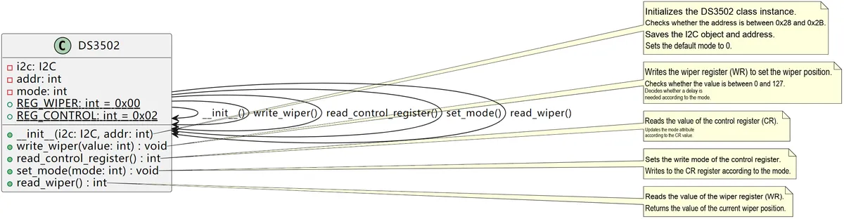
- Initialization
__init__method: Here, we only need to pass in the I2C interface object and the I2C address of the DS3502. First, we perform an address range check to ensure that the address is between0x28and0x2B(i. e., between 0101000 and 0101011 in binary), otherwise aValueErrorexception will be thrown; meanwhile, the I2C object and address are saved, andmodeis initialized to0. Themodecontrols the data writing mode, where0indicates slow mode and1indicates fast mode. - Set the value of the wiper register
write_wiperMethod: This method changes the resistance value of the potentiometer by writing to the wiper register. First, an input range check is performed to ensure thatvalueis in the range from0to127; then thewriteto_memmethod is used to writevalueto theREG_WIPERregister to update the position of the potentiometer. Meanwhile, ifmodeis0(slow mode), a delay of100msis executed - Read control register value
read_control_registerMethod: Mainly by reading the value of the control registerCRto check themodestatus. This method uses thereadfrom_memmethod to read the value ofREG_CONTROL; if the read data is0x80, it indicates that the current mode is1, then updateself.modeto1and return the current mode. - Set control register mode
set_modeMethod: Primarily based on themodeparameter, set the value of the control register. First, ensure thatmodeis either0or1; otherwise, throw aValueError. Then, write the register value corresponding to the respective mode to the control register addressREG_CONTROL, and setself.modeto the current mode. - Read the value of the wiper register
read_wiperMethod: The main function is to read the current value of the wiper register, which uses thereadfrom_memmethod to read data fromREG_WIPER.
2.3 Custom Class of AD9833
In the following code, we customize an AD9833 class to control the AD9833 waveform generator chip, which sends configuration commands to the AD9833 via the SPI Communication Protocol to generate the required waveforms.
The sample code is as follows:
# Python env   : MicroPython v1.23.0
# -*- coding: utf-8 -*-
# @Time    : 2024/9/3 2:20 PM
# @Author  : Li Qingshui
# @File    : ad9833.py
# @Description : Driver module for the AD9833 DDS signal chip
# Code reference: https://github.com/owainm713/AD9833-MicroPython-Module/blob/main/AD9833example.py#L54
# This part of the code was developed by owainm713 and is licensed under the GNU General Public License v3.0.

# ======================================== Import Modules =========================================

# Import hardware-related modules
import machine
# Import digital signal processing related modules
from math import pi, radians

# ======================================== Global Variables ============================================

# ======================================== Functions ============================================

# ======================================== Custom Classes ============================================

# Custom class for the AD9833 DDS signal chip
class AD9833:
    """
    The AD9833 class is used to control the AD9833 waveform generator chip, communicating with the main controller over the SPI interface to configure the output waveform, frequency, and phase.

    This class provides various functions for controlling the AD9833, including setting the output waveform type (sine, square, triangle), adjusting frequency and phase, and allowing the waveform parameters to be modified dynamically at runtime.

    Attributes:
        fmclk (int): Master clock frequency in Hz, default 25MHz.
        sdo (machine.Pin): SPI data output pin, used to transmit data.
        clk (machine.Pin): SPI clock pin, controlling the timing of data transmission.
        cs (machine.Pin): SPI chip select pin, used to select the AD9833 chip.
        spi (machine.SPI): SPI communication object, used for data transfer with the AD9833.
        mode (str): Current mode, default "RESET", controlling the working state of the AD9833.
        writeMode (str): Write mode, default is writing both MSB and LSB, used to set frequency and phase.
        freq0 (int): Value of frequency register 0, used to store the set frequency.
        freq1 (int): Value of frequency register 1, used to store the set frequency.
        phase0 (int): Value of phase register 0, used to control the signal phase.
        phase1 (int): Value of phase register 1, used to control the signal phase.

    Methods:
        __init__(self, sdo: int, clk: int, cs: int, fmclk: int = 25, spi_id: int = 0):
            Initialize an AD9833 instance and set the SPI communication object and master clock frequency.

        set_control_reg(**kwargs) -> None:
            Set the control register of the AD9833 to control the chip's operating mode, such as reset and waveform type.

        write_data(data: int) -> None:
            Write the specified data to the AD9833.

        set_frequency(reg: int, freq: int) -> None:
            Set the frequency register of the AD9833 to control the frequency of the output waveform.

        set_phase(reg: int, phase: int) -> None:
            Sets the AD9833 phase register, which controls the phase of the output waveform.

        reset() -> None:
            Resets the AD9833 and reinitializes all registers and settings.
    """

    def __init__(self, sdo: int, clk: int, cs: int, fmclk: int = 25, spi_id: int = 0) -> None:
        """
        Initializes the AD9833 instance.

        This method initializes the basic settings of the AD9833 module, including the SPI communication pins and the master clock frequency.

        Args:
            sdo (int): Pin number for SDATA.
            clk (int): Pin number for CLK.
            cs (int): Pin number for CS.
            fmclk (int, optional): Master clock frequency. The actual operating frequency is fmclk MHz. Defaults to 25 MHz.
            spi_id (int, optional): SPI peripheral number. Defaults to 0, which means the first SPI peripheral is used.

        Returns:
            None: This method has no return value.

        Raises:
            ValueError: Raised if the sdo, clk, or cs arguments are not valid numeric pin numbers or the spi peripheral number is invalid.
        """

        # If the sdo, clk, or cs arguments are not numeric pin numbers, raise an error
        if not isinstance(sdo, int) or not isinstance(clk, int) or not isinstance(cs, int):
            raise ValueError("sdo、clk、cs must be int")

        # Check whether spi_id is valid
        if spi_id not in (0, 1):
            raise ValueError("spi_id must be 0 or 1")

        # Set the clock frequency (default is 25 MHz)
        self.fmclk = fmclk * 10 ** 6

        # Set the SPI pin parameters
        self.sdo = machine.Pin(sdo)
        self.clk = machine.Pin(clk)
        self.cs = machine.Pin(cs, machine.Pin.OUT)
        # Initialize the chip select pin to high, meaning communication has not started
        self.cs.value(1)
        # Set the SPI communication parameters
        self.spi = machine.SPI(spi_id, baudrate=1000000, polarity=0, phase=1, sck=self.clk, mosi=self.sdo)
        # Initialize the control register to the reset state, with the frequency register write mode set to 28-bit data write
        self.set_control_reg(B28=1, RESET=1)

        # Initialize the mode to reset
        self.mode = "RESET"
        # Initialize the write mode to write MSB and LSB together
        self.writeMode = "BOTH"
        # Initialize the values of frequency register 0 and register 1
        self.freq0 = 0
        self.freq1 = 0
        # Initialize the values of phase register 0 and register 1
        self.phase0 = 0
        self.phase1 = 0

    def write_data(self, data: int) -> None:
        """
        Writes data to an AD9833 register.

        This method writes the given integer data to an AD9833 register in order to update its configuration or control the waveform.

        The chip's SPI communication mode uses CPOL = 0, CPHA = 1, i.e. SPI Mode 1, and FSYNC (frame sync) is not held low all the time like a standard SPI chip select (CS), but instead
        is pulled low briefly before each frame of data is transferred. SCLK only starts transferring data after FSYNC goes low, and unlike standard SPI it cannot run as a continuous clock. Its protocol is more like I²S, TDM, or an SPI variant specific to certain DSP devices.
        Simply put, before each data write we need to manually pull SCLK high and then pull the chip select pin low to start communication.

        Args:
            data (int): Data to write to the AD9833 register. Must be an integer.

        Returns:
            None: This method has no return value.

        Raises:
            ValueError: Raised if the data argument is not an integer.
        """

        # Convert the data to a byte array
        data = bytearray(data)

        # Manually pull SCLK high
        self.clk.value(1)
        # Pull the chip select pin low to start communication
        self.cs.value(0)
        # Adjust the SPI rate
        self.spi.init(baudrate=1000000)
        # Write data over SPI
        self.spi.write(data)
        # Pull the chip select pin high to end communication
        self.cs.value(1)

        return

    def set_control_reg(self, B28: int = 1, HLB: int = 0, FS: int = 0, PS: int = 0,
                        RESET: int = 0, SLP1: int = 0, SLP12: int = 0, OP: int = 0, DIV2: int = 0, MODE: int = 0) -> None:
        """
        Sets the individual bit values of the control register to configure the working state of the AD9833.

        Based on the given arguments, this method sets the individual bits in the AD9833 control register to control the device's reset state, output mode, frequency register, phase register, and other functions.

        Args:
            B28 (int, optional): Sets the B28 bit, used for the frequency register write mode. Defaults to 1.
            HLB (int, optional): Sets the HLB bit, used for high/low byte switching. Defaults to 0.
            FS (int, optional): Sets the FS bit, which selects the frequency register. Defaults to 0.
            PS (int, optional): Sets the PS bit, which selects the phase register. Defaults to 0.
            RESET (int, optional): Sets the RESET bit, which controls the reset state. Defaults to 0.
            SLP1 (int, optional): Sets the SLP1 bit, used for sleep mode. Defaults to 0.
            SLP12 (int, optional): Sets the SLP12 bit, used for sleep mode. Defaults to 0.
            OP (int, optional): Sets the OP bit, used for output mode selection. Defaults to 0.
            DIV2 (int, optional): Sets the DIV2 bit, which halves the output frequency. Defaults to 0.
            MODE (int, optional): Sets the MODE bit, which selects the output waveform mode. Defaults to 0.

        Returns:
            None: This method has no return value.

        Raises:
            ValueError: Raised if any argument is not an integer value of 0 or 1.
        """

        # If an input register argument is not 0 or 1, raise an exception
        if B28 != 0 and B28 != 1:
            raise ValueError("B28 must be 0 or 1")
        if HLB != 0 and HLB != 1:
            raise ValueError("HLB must be 0 or 1")
        if FS != 0 and FS != 1:
            raise ValueError("FS must be 0 or 1")
        if PS != 0 and PS != 1:
            raise ValueError("PS must be 0 or 1")
        if RESET != 0 and RESET != 1:
            raise ValueError("RESET must be 0 or 1")
        if SLP1 != 0 and SLP1 != 1:
            raise ValueError("SLP1 must be 0 or 1")
        if SLP12 != 0 and SLP12 != 1:
            raise ValueError("SLP12 must be 0 or 1")
        if OP != 0 and OP != 1:
            raise ValueError("OP must be 0 or 1")
        if DIV2 != 0 and DIV2 != 1:
            raise ValueError("DIV2 must be 0 or 1")
        if MODE != 0 and MODE != 1:
            raise ValueError("MODE must be 0 or 1")

        # Set the control register parameters
        self.B28 = B28
        self.HLB = HLB
        self.FS = FS
        self.PS = PS
        self.RESET = RESET
        self.SLP1 = SLP1
        self.SLP12 = SLP12
        self.OP = OP
        self.DIV2 = DIV2
        self.MODE = MODE

        # Concatenate all bits into the control register value
        controlReg = (B28 << 13) + (HLB << 12) + (FS << 11) + (PS << 10) + (RESET << 8) + (SLP1 << 7) + (SLP12 << 6) + (
                    OP << 5) + (DIV2 << 3) + (MODE << 1)

        # Split the control register value into two bytes and send them with two SPI writes
        controlRegList = [(controlReg & 0xFF00) >> 8, controlReg & 0x00FF]
        # Write the control register data
        self.write_data(controlRegList)

        return

    def set_frequency(self, fout: int, freqSelect: int) -> None:
        """
        Sets the value of the frequency register, selecting and updating the AD9833 output frequency.

        Based on the given output frequency and the selected frequency register, calculates and updates the AD9833 frequency register. Frequency register 0 or 1 can be selected for the update.

        Args:
            fout (int): Desired signal output frequency in Hz, in the range 0 to 12.5MHz.
            freqSelect (int): Selects the frequency register to write to. Value is 0 or 1, meaning frequency register 0 or 1.

        Returns:
            None: This method has no return value.

        Raises:
            ValueError: Raised if the given `freqSelect` is not 0 or 1, or if `fout` is not within the valid frequency range (0 to 12.5MHz).
        """
        # If freqSelect is not 0 or 1, raise an exception
        if freqSelect != 0 and freqSelect != 1:
            raise ValueError("freqSelect must be 0 or 1")

        # Check whether the input frequency is between 0 and 12.5MHz; if not, raise an exception
        if fout < 0 or fout > 12500000:
            raise ValueError("fout must be 0 to 12.5MHz")

        # Calculate the value to write to the frequency register
        freqR = int((fout * pow(2, 28)) / self.fmclk)

        # Split the frequency register value into two 14-bit segments: fMSB (upper 14 bits) and fLSB (lower 14 bits)
        fMSB = (freqR & 0xFFFC000) >> 14
        fLSB = freqR & 0x3FFF

        # Add the register address to each 14-bit segment
        if freqSelect == 0:
            # Select frequency register 0
            addr = 0b01
            # Store the set frequency value
            self.freq0 = fout
        else:
            # Select frequency register 1
            addr = 0b10
            # Store the set frequency value
            self.freq1 = fout

        # Add the register address to the upper 14-bit segment
        fMSB = fMSB + (addr << 14)
        # Add the register address to the lower 14-bit segment
        fLSB = fLSB + (addr << 14)

        # Split fMSB and fLSB each into two 8-bit segments
        fLSBList = [(fLSB & 0xFF00) >> 8, fLSB & 0x00FF]
        fMSBList = [(fMSB & 0xFF00) >> 8, fMSB & 0x00FF]
        fBoth = fLSBList + fMSBList

        # Write only the upper 14 bits
        if self.writeMode == 'MSB':
            self.write_data(fMSBList)
        # Write only the lower 14 bits
        elif self.writeMode == 'LSB':
            self.write_data(fLSBList)
        # Write all 14 bits
        else:
            self.write_data(fBoth)

        return

    def set_phase(self, pout: int, phaseSelect: int, rads: bool = True) -> None:
        """
        Sets the value of the phase register, selecting and updating the AD9833 output phase.

        Based on the given phase value, the selected phase register, and whether radians are used, calculates and updates the AD9833 phase register. Phase register 0 or 1 can be selected for the update.

        Args:
            pout (int): Desired signal output phase, in degrees (if rads is False) or radians (if rads is True).
            phaseSelect (int): Selects the phase register to write to. Value is 0 or 1, meaning phase register 0 or 1.
            rads (bool): Whether to treat the input phase value as radians (default True). If False, the input value is in degrees.

        Returns:
            None: This method has no return value.

        Raises:
            ValueError: Raised if the given `phaseSelect` is not 0 or 1.
        """

        # If phaseSelect is not 0 or 1, raise an exception
        if phaseSelect != 0 and phaseSelect != 1:
            raise ValueError("phaseSelect must be 0 or 1")

        # Calculate the value of the phase register
        if rads == False:
            # Convert degrees to radians
            pout = radians(pout)

        # Calculate the phase register value from radians
        phaseR = int(pout * 4096 / (2 * pi))

        # Combine the phase value with the address
        phaseR = phaseR + (0b11 << 14) + (phaseSelect << 13)

        # Split phaseR into 8-bit segments
        phaseRList = [(phaseR & 0xFF00) >> 8, phaseR & 0x00FF]

        # Write the phase register data
        self.write_data(phaseRList)

        return

    def set_mode(self, mode: str = 'SIN') -> None:
        """
        Sets the type of waveform output by the AD9833, selecting different waveforms according to the input mode.

        Sets the waveform type of the AD9833 output signal based on the given `mode` argument. Supported waveforms are: sine wave, triangle wave, square wave, half-frequency square wave, reset, and off mode.

        Args:
            mode (str): Selects the output waveform type. Supported values are:
                - 'SIN': sine wave
                - 'TRIANGLE': triangle wave
                - 'SQUARE': square wave
                - 'SQUARE/2': half-frequency square wave
                - 'RESET': reset mode
                - 'OFF': off mode (puts the device into a low-power state)

                Default is 'SIN' (sine wave).

        Returns:
            None: This method has no return value.

        Raises:
            ValueError: Raised if the `mode` argument is not among the supported options.
        """

        # Check whether the input waveform mode is SIN, TRIANGLE, SQUARE, SQUARE/2, RESET, or OFF
        if mode != 'SIN' and mode != 'TRIANGLE' and mode != 'SQUARE' and mode != 'SQUARE/2' and mode != 'RESET' and mode != 'OFF':
            raise ValueError("mode must be 'SIN', 'TRIANGLE', 'SQUARE', 'SQUARE/2', 'RESET' or 'OFF'")

        # Store the current mode
        self.mode = mode

        # Sine wave mode
        if mode == 'SIN':
            self.set_control_reg(B28=self.B28, HLB=self.HLB, FS=self.FS, PS=self.PS, RESET=0, MODE=0)
        # Triangle wave mode
        elif mode == 'TRIANGLE':
            self.set_control_reg(B28=self.B28, HLB=self.HLB, FS=self.FS, PS=self.PS, RESET=0, MODE=1)
        # Square wave mode
        elif mode == 'SQUARE':
            self.set_control_reg(B28=self.B28, HLB=self.HLB, FS=self.FS, PS=self.PS, RESET=0, SLP12=1,
                                 OP=1, DIV2=1, MODE=0)
        # Half-frequency square wave mode
        elif mode == 'SQUARE/2':
            self.set_control_reg(B28=self.B28, HLB=self.HLB, FS=self.FS, PS=self.PS, RESET=0, SLP12=1,
                                 OP=1, DIV2=0, MODE=0)
        # Reset mode
        elif mode == 'RESET':
            self.set_control_reg(B28=self.B28, HLB=self.HLB, FS=self.FS, PS=self.PS, RESET=1)
        # Off mode
        elif mode == 'OFF':
            self.set_control_reg(B28=self.B28, HLB=self.HLB, FS=self.FS, PS=self.PS, RESET=1, SLP1=1, SLP12=1)

        return

    def set_write_mode(self, writeMode: str = 'BOTH') -> None:
        """
        Sets the write mode of the frequency register.

        This method configures how the frequency register is written. Three modes are supported:
        - 'BOTH': write MSB and LSB together;
        - 'MSB': write only the upper 14 bits (MSB);
        - 'LSB': write only the lower 14 bits (LSB).

        Args:
            writeMode (str): Write mode. Supported options are:
                - 'BOTH': write both the MSB and LSB of the frequency register;
                - 'MSB': write only the upper 14 bits of the frequency register;
                - 'LSB': write only the lower 14 bits of the frequency register.
                Default is 'BOTH'.

        Returns:
            None: This method has no return value.

        Raises:
            ValueError: Raised if the `writeMode` argument is not among the supported options.
        """

        # Check whether the write mode is BOTH, MSB, or LSB; if not, raise an exception
        if writeMode != 'BOTH' and writeMode != 'MSB' and writeMode != 'LSB':
            raise ValueError("writeMode must be 'BOTH', 'MSB' or 'LSB'")

        # Initialize the B28 bit to 1, meaning both the MSB and LSB of the frequency register are written together
        B28 = 1
        # Initialize the HLB bit to 0, selecting which part to write; the default is to write all
        HLB = 0
        # The default write mode is 'BOTH', i.e. write MSB and LSB together
        self.writeMode = 'BOTH'

        #  If the write mode is 'MSB', write only the upper 14 bits of the frequency register
        if writeMode == 'MSB':
            # Set the B28 bit to 0 and HLB to 1
            B28 = 0
            HLB = 1
            self.writeMode = 'MSB'
        # If the write mode is 'LSB', only the lower 14 bits of the frequency register are written
        elif writeMode == 'LSB':
            # Set bit B28 to 0 and HLB to 0
            B28 = 0
            HLB = 0
            self.writeMode = 'LSB'

        # Update the control register according to the selected B28 and HLB bits
        self.set_control_reg(B28=B28, HLB=HLB, FS=self.FS, PS=self.PS, RESET=self.RESET, SLP1=self.SLP1,
                             SLP12=self.SLP12, OP=self.OP, DIV2=self.DIV2, MODE=self.MODE)

        return

    def select_freq_phase(self, FS: int, PS: int) -> None:
        """
        Select the frequency register and the phase register.

        This method updates the control register according to the given frequency register select (FS) and phase register select (PS).
        The selected registers will be used for subsequent frequency and phase settings.

        Args:
            FS (int): Selects the frequency register. Valid values are 0 or 1, indicating different parts of the frequency register.
            PS (int): Selects the phase register. Valid values are 0 or 1, indicating different parts of the phase register.

        Returns:
            None: This method has no return value.

        Raises:
            ValueError: Raised if the value of `FS` or `PS` is outside the valid range (that is, not 0 or 1).
        """

        # Check whether the input FS is 0 or 1; raise an exception if not
        if FS != 0 and FS != 1:
            raise ValueError("FS must be 0 or 1")
        # Check whether the input PS is 0 or 1; raise an exception if not
        if PS != 0 and PS != 1:
            raise ValueError("PS must be 0 or 1")

        # Update the control register according to the specified frequency select (FS) and phase select (PS)
        self.set_control_reg(B28=self.B28, HLB=self.HLB, FS=FS, PS=PS, RESET=self.RESET, SLP1=self.SLP1,
                             SLP12=self.SLP12, OP=self.OP, DIV2=self.DIV2, MODE=self.MODE)

        return

# ======================================== Initialization ==========================================

# ========================================  Main Program  ===========================================
The custom AD9833 class we defined includes the following methods:
- Initialization method
init: It takes the used pin number, SPI peripheral number and clock frequency (in MHz) as input, completes the initialization of pins and peripheral functions, and calls theset_control_regmethod to configure the control register, so as to put the AD9833 into reset state, enable the 28-bit frequency register write mode, and meanwhile set the initial values of both the frequency register and the phase register to 0.
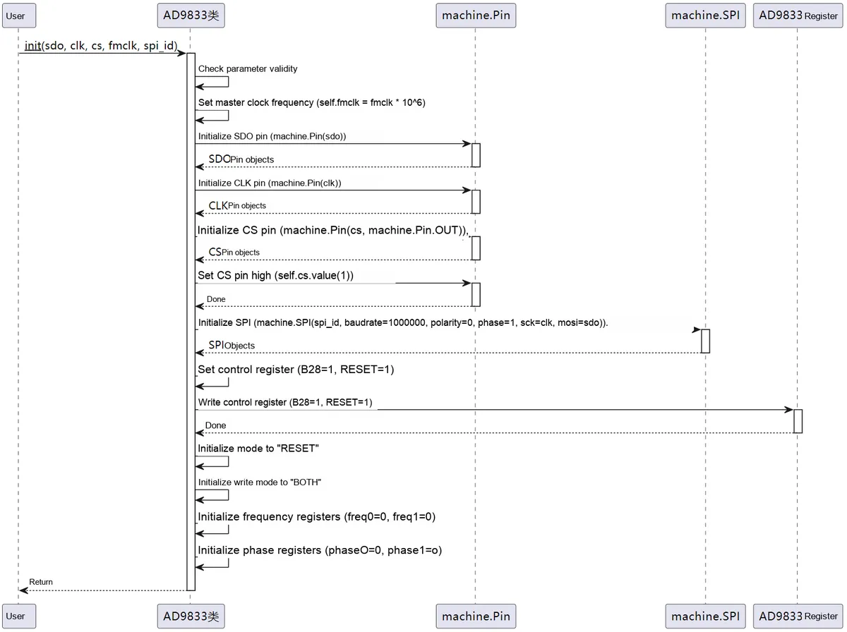
- SPI Data Writing Method
write_data: Convert the data to be written to the AD9833 into a byte array format. First, manually pull the SPI clock pin (SCLK) high to prepare for communication, then pull the CS pin low to initiate SPI communication and send the data to the AD9833 chip, and pull the CS pin high when the communication ends.
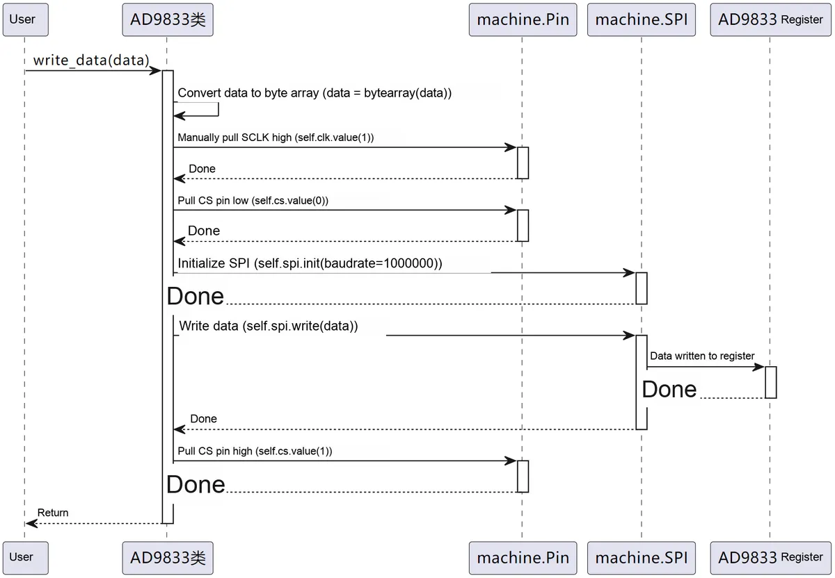
- Control Register Configuration Method
set_control_reg: Generates the 16-bit value of the control register according to the set data bits, splits the 16-bit value of the control register into two 8-bit bytes, and sends them to the AD9833 via thewrite_datamethod. The reason for splitting the 16-bit value of the control register into two 8-bit bytes is that the SPI peripheral in MicroPython defaults to an 8-bit data frame length.
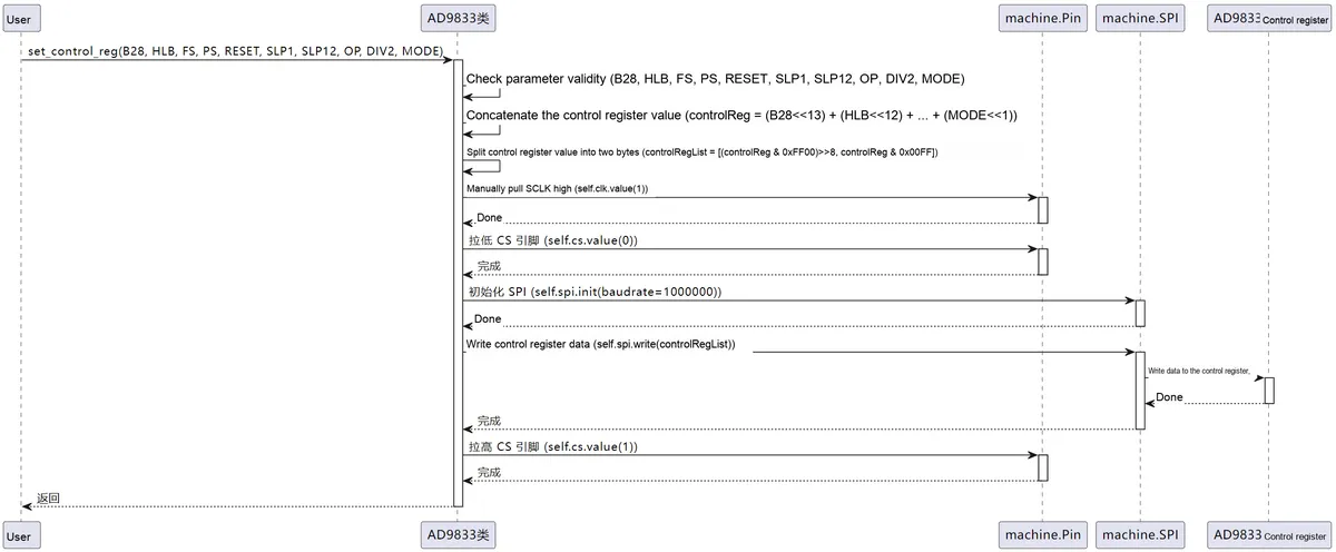
- Frequency Setting Method
set_frequency: This method calculates the frequency register value to be written to the AD9833, splits the calculated frequency register value into the upper 14 bits and the lower 14 bits, then selects frequency register 0 or 1 according tofreqSelect, splits each of the upper 14 bits and lower 14 bits into two 8-bit bytes, and writes them to the AD9833 via thewrite_datamethod.
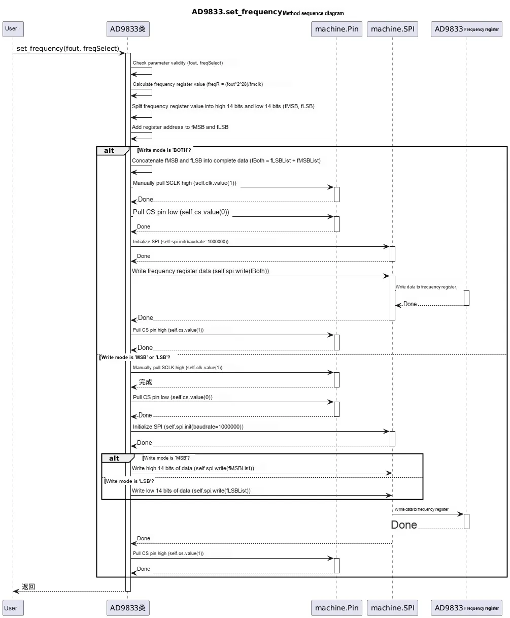
- Phase Setting Method
set_phase: Calculate the value of the phase register to be written according to the phase value, then split the calculated phase register value into two 8-bit bytes, and write them to the AD9833 via thewrite_datamethod.
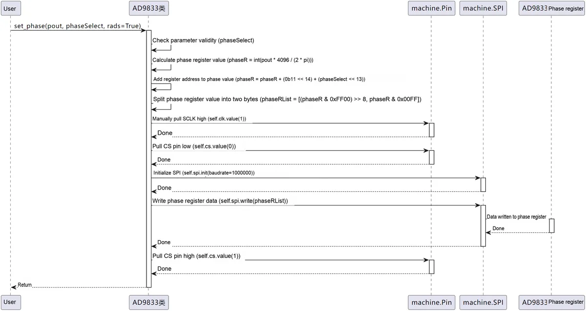
- Output waveform type setting method
set_mode: According to the selected waveform type, configure different bits of the control register and call the control register setting methodset_control_regto set the output mode of the AD9833, which can select modes such as sine wave (SIN), triangle wave (TRIANGLE), square wave (SQUARE), square wave with half amplitude (SQUARE/2), reset (RESET), and off (OFF).
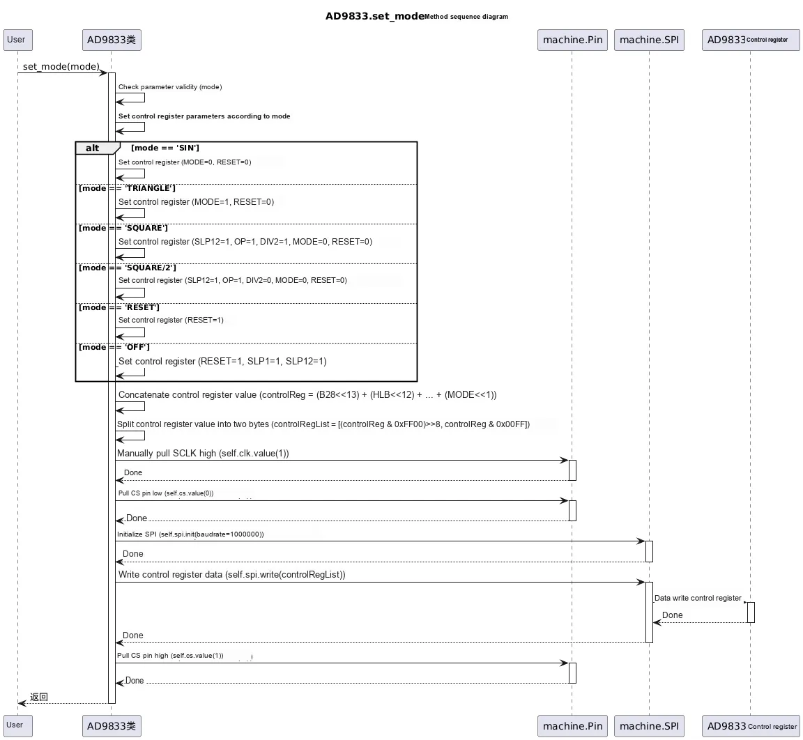
- Frequency Register Write Mode Configuration Method
set_write_mode: Adjust the write mode of the frequency register according to the selected write mode; wherein,BOTHindicates simultaneous writing to both the upper 14 bits and the lower 14 bits,MSBindicates writing only to the upper 14 bits,LSBindicates writing only to the lower 14 bits.
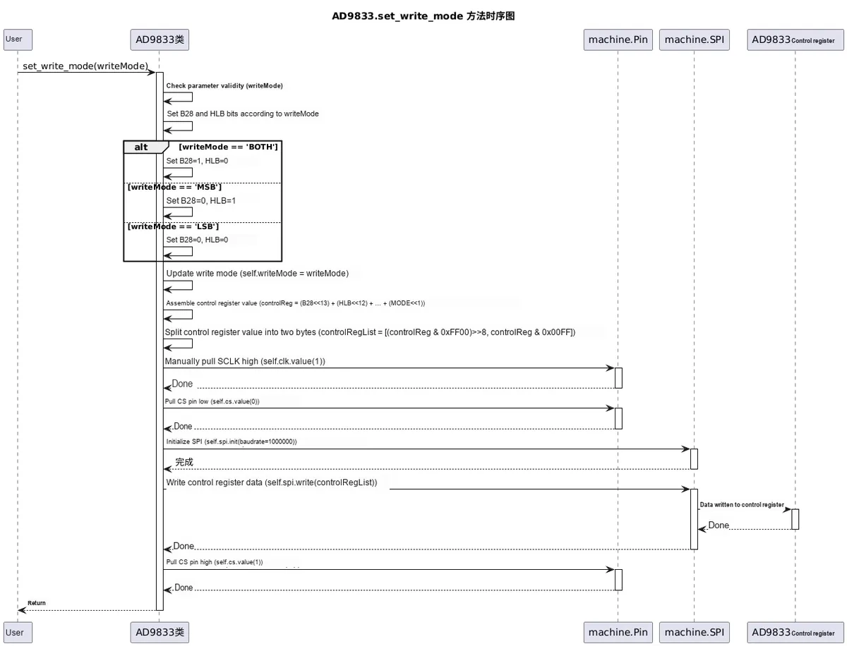
- Frequency Register and Phase Register Selection Method
select_freq_phase: selects which frequency register and phase register to use; both of them have optional parameters of 0 or 1, then useset_control_regto set the data bits of the control register and write them to the AD9833 via thewrite_datamethod.
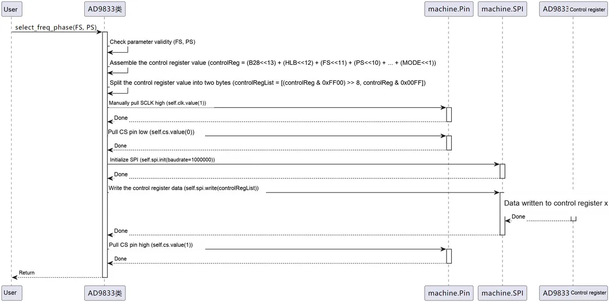
The internal method calls within the AD9833 class are as follows:
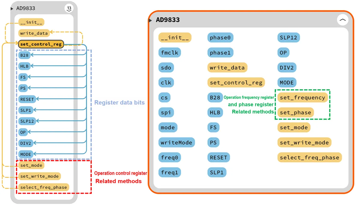
Combined with our source code, it can be seen that its methods can basically be divided into two major categories:
- Related methods of the operation control register: Such methods include
set_control_reg,set_mode,set_write_modeandset_write_mode. The basic idea of such methods is to first set the corresponding data bits, then pass the configured data bits to the control register setting methodset_control_reg, andset_control_regorganizes and splits the data bits, then sends the register bits to the AD9833 via thewrite_datamethod. - Related methods for operation frequency and phase registers: Such methods include
set_frequencyandset_phase. The basic idea is to first perform data conversion on the input frequency or phase value, and then write it to the AD9833 via thewrite_datamethod.
When using the AD9833 class, we first need to create an instance of the AD9833 class, configure the SPI pins and clock frequency, and then: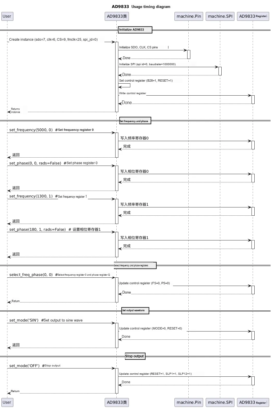
- Set the frequency and phase of the signal to be output via the
set_frequencymethod and theset_phasemethod. - Use
the select_freq_phasemethod to select which frequency register and phase register to use; the selected frequency register and phase register must be the ones we have configured previously. - Use the
set_modemethod to select the type of waveform to be output, and then a waveform will be output from the Vout terminal. - When the AD9833 is not in use temporarily, you can use
set_mode ('OFF')to stop the waveform output at the Vout terminal.
2.4 Custom Class for MCP41010
In the following code, we implement the function of controlling the output value of the potentiometer chip MCP41010 or entering its shutdown mode by sending command and data bytes via the SPI communication interface. The sample code is shown as follows:
# Python env   : MicroPython v1.23.0
# -*- coding: utf-8 -*-
# @Time    : 2024/12/27 11:09 AM
# @Author  : Li Qingshui
# @File    : mcp41010.py
# @Description : Driver for the MCP41010 digital potentiometer chip
# This part of the code was developed by leeqingshui and is licensed under CC BY-NC 4.0.

# ======================================== Import Modules =========================================

# Hardware-related modules
from machine import Pin, SPI

# ======================================== Global Variables ============================================

# ======================================== Functions ============================================

# ======================================== Custom Classes ============================================

# Custom class for the MCP41010 single-channel digital potentiometer
class MCP41010:
    """
    The MCP41010 class controls the MCP41010 single-channel digital potentiometer, communicating with the host chip over the SPI interface to adjust the potentiometer value.

    Attributes:
        cs (Pin): GPIO object used to control the chip select pin.
        spi (SPI): SPI interface object used to communicate with the MCP41010.
        max_value (int): Maximum adjustment value of the potentiometer, default 255.

    Methods:
        __init__(clk_pin: int, cs_pin: int, mosi_pin: int, spi_id: int = 0, max_value: int = 255) -> None:
            Initialize the MCP41010 instance and configure the SPI interface and the maximum potentiometer value.

        set_value(value: int) -> None:
            Set the MCP41010 potentiometer value, in the range 0 to max_value.

        set_shutdown() -> None:
            Put the MCP41010 potentiometer into shutdown mode to reduce power consumption.

        _send_command(command_byte: int, data_byte: int) -> None:
            Send 16-bit data over SPI to perform MCP41010 operations (such as setting the potentiometer value, shutdown mode, etc.).
    """

    def __init__(self, clk_pin: int, cs_pin: int, mosi_pin: int, spi_id: int = 0, max_value: int = 255) -> None:
        """
        Initialize the MCP41010 instance.

        This method initializes the SPI interface and chip select pin of the MCP41010 digital potentiometer and configures the communication parameters.

        Args:
            clk_pin (int): GPIO number of SCK (clock pin), used to provide the clock signal.
            cs_pin (int): GPIO number of CS (chip select pin), used to select this device for communication.
            mosi_pin (int): GPIO number of MOSI (master out, slave in pin), used to transmit data.
            spi_id (int, optional): SPI peripheral ID, default 0, meaning the first SPI peripheral is used.
            max_value (int, optional): Maximum value of the potentiometer, default 255, meaning the maximum adjustment value of the potentiometer.

        Returns:
            None: This method has no return value.

        Raises:
            None: This method does not raise exceptions.
        """
        # Initialize the CS pin as output
        self.cs = Pin(cs_pin, Pin.OUT)
        # Initialize CS to high level
        self.cs.value(1)

        # SPI peripheral used
        self.spi = SPI(spi_id,
                       baudrate=1000000,    # SPI clock frequency (1 MHz)
                       polarity=0,          # Clock idles low
                       phase=0,             # Data is sampled on the rising clock edge
                       sck=Pin(clk_pin),    # Clock SCK pin
                       mosi=Pin(mosi_pin))  # Data MOSI pin
        self.max_value = max_value

    def set_value(self, value: int) -> None:
        """
        Set the potentiometer value of the MCP41010.

        This method sets the output value of the MCP41010 digital potentiometer. The potentiometer value should be between 0 and the maximum value.

        Args:
            value (int): Potentiometer value, which should be in the range 0 to `max_value`.

        Returns:
            None: This method has no return value.

        Raises:
            ValueError: Raised if the input value is outside the valid range (0 to `max_value`).
        """

        # Check whether the input value is within the valid range
        if value < 0 or value > self.max_value:
            raise ValueError("Value must be between 0 and %d" % self.max_value)

        # Command byte: C1=0, C0=1 (write data), P1=0, P0=1 (potentiometer select)
        command_byte = 0b00010001
        data_byte = value
        self._send_command(command_byte, data_byte)

    def set_shutdown(self) -> None:
        """
        Put the potentiometer into shutdown mode.

        This method puts the MCP41010 digital potentiometer into shutdown mode to reduce power consumption.

        Args:
            None

        Returns:
            None: This method has no return value.
        """

        # Command byte: C1=1, C0=0 (shutdown mode), P1=0, P0=1 (potentiometer select)
        command_byte = 0b00100001
        # The data bits are "don't care" bits
        data_byte = 0x00
        self._send_command(command_byte, data_byte)

    def _send_command(self, command_byte: int, data_byte: int) -> None:
        """
        Send 16-bit data over SPI.

        This method sends a 16-bit command and data byte over the SPI bus to communicate with the MCP41010 digital potentiometer.

        Args:
            command_byte (int): First 8-bit command byte, specifying the operation type (such as write data, shutdown mode, etc.).
            data_byte (int): Last 8-bit data byte, representing the actual data or parameter of the operation (such as the potentiometer value).

        Returns:
            None: This method has no return value.
        """

        # Pull CS low to start communication
        self.cs.value(0)
        # Adjust the SPI rate
        self.spi.init(baudrate=1000000)
        # Write 16-bit data
        self.spi.write(bytearray([command_byte, data_byte]))
        # Pull CS high to end communication
        self.cs.value(1)

# ======================================== Initialization ==========================================

# ========================================  Main Program  ===========================================
The custom MCP41010 class we defined includes the following methods:
__init__Method: First, initialize the chip select pincsto output mode and set it to high level (the chip is not selected by default), then initialize the SPI interface, set the clock frequency to 1 MHz, the polarity to 0 (low level when the clock is idle), the phase to 0 (data is sampled on the rising edge of the clock), and set the maximum value of the potentiometer at the same timemax_value, which defaults to 255._send_commandMethod: This method implements sending 16-bit data (command byte + data byte) via SPI. First, pull down the chip select pincsto start SPI communication;Then initialize the SPI and set the baud rate to 1 MHz. Since SPI is a bus communication protocol, devices with different communication rates may be mounted on the same bus, so we callspi.init (baudrate= 1000000)again here to ensure that the SPI works at the correct rate every time data is sent, without being affected by the initialization of other devices; after sending 16-bit data (command byte + data byte), pull up the chip select pincsto terminate the SPI communication.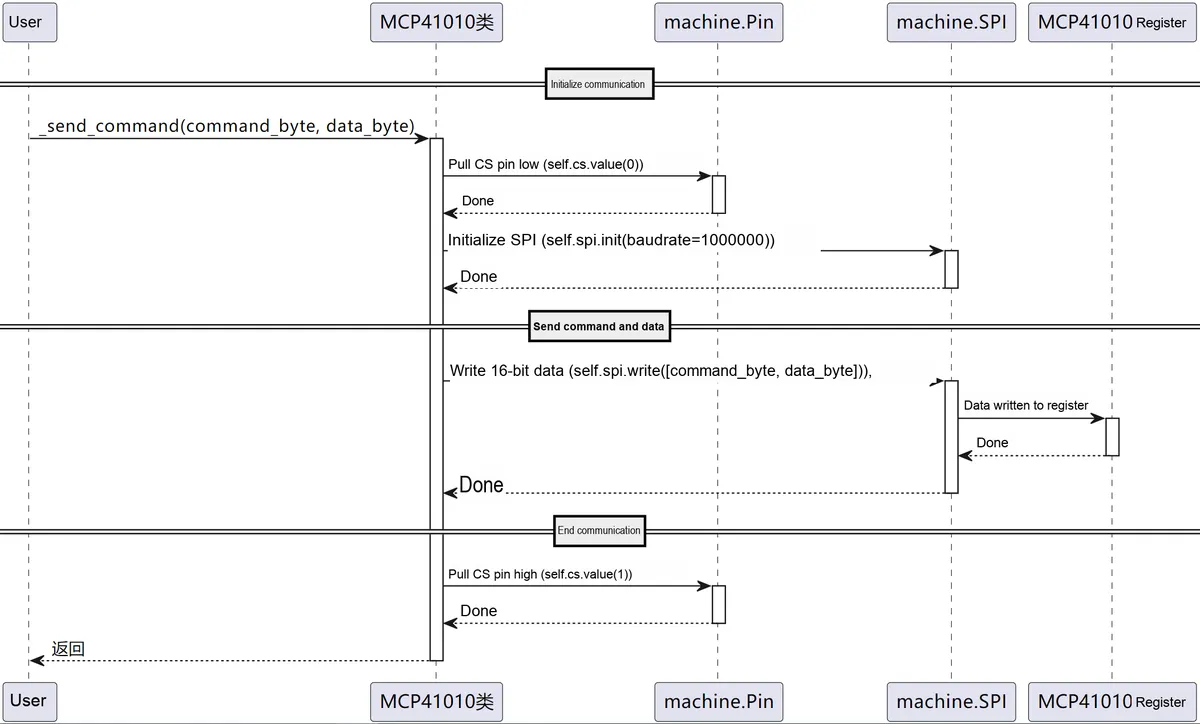
The methods for setting the resistance value of the potentiometer, namely
set_value, and for setting the shutdown mode, namelyset_shutdown, are both implemented by calling the SPI data transmission_send_commandmethod.set_valuemethod: First, check whether the input potentiometer value to be set falls within the valid range (0 tomax_value). If the value is out of range, aValueErrorwill be thrown. Next, construct the command byte0b00010001, then call the_send_commandmethod to send the command byte and the data byte (the potentiometer value).
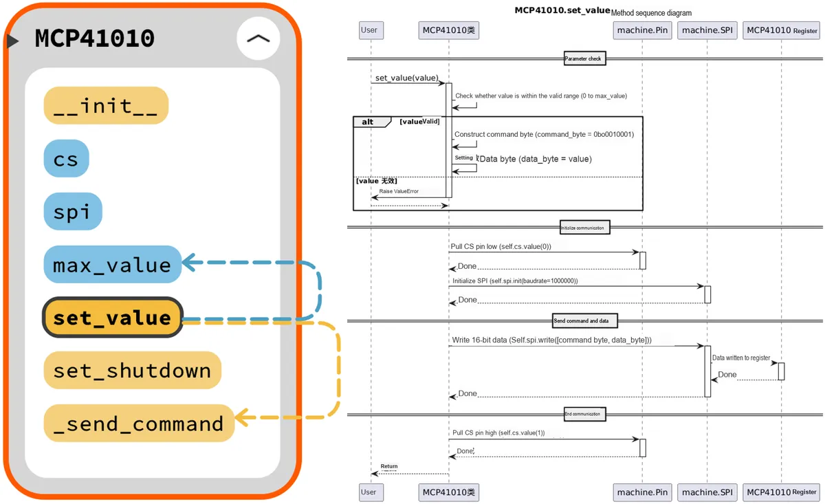
set_shutdownMethod: Construct the command byte0b00100001, set the data byte (don't-care bits) to0x00, then call the_send_commandmethod to send the command byte and the data byte.
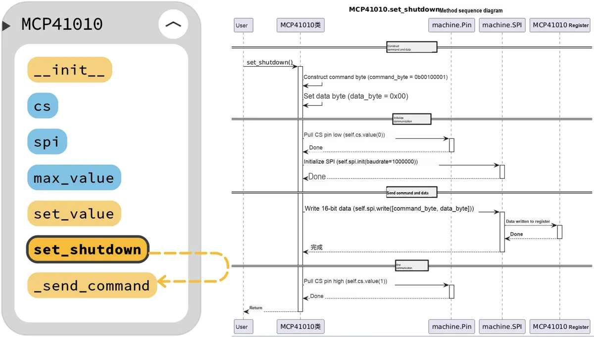
3. Application Examples
3.1 Generating Sine Waves with the MCP4725
In the following experiment, we need to insert the Fengya No. 1 Board - Data Conversion Board into the Fengya No. 1 Board - Universal Compatible Expansion Board, and at the same time turn on the SCL, SDA and RDY options of the DIP switch SWITCH1 on the Fengya No. 1 Board - Data Conversion Board, and also turn on the ADC1 switch option of the DIP switch SWITCH2:
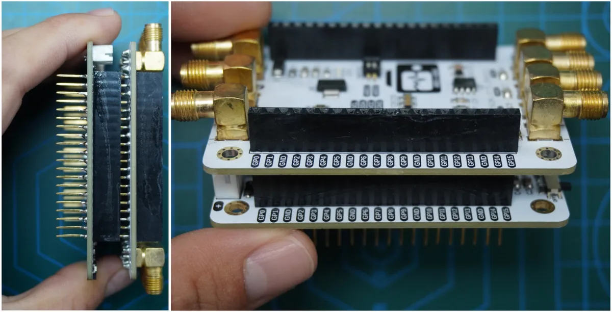
Additionally, please select an address on the MCP4725 chip address selection A0 DIP switch (only one option can be toggled). In this example, we will toggle the GND switch to the ON position, so the MCP4725 chip's I²C address is 0x60:
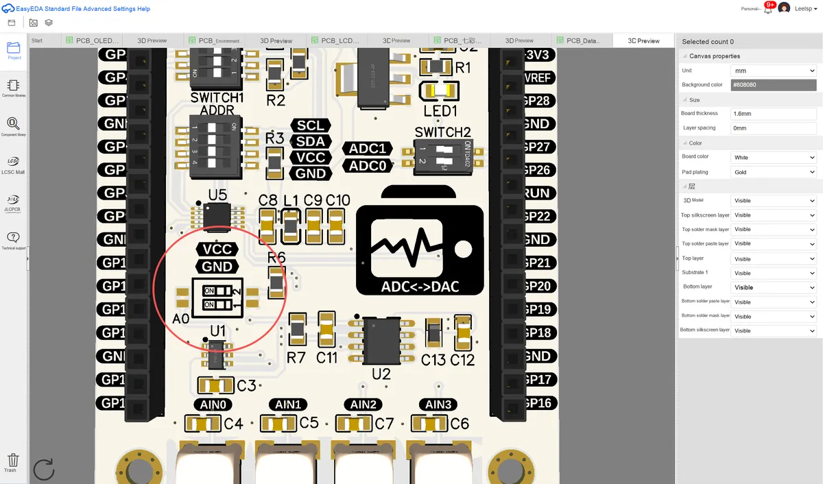
In addition, we first need to connect the MiniUSB data cable to the serial port on Fengya No. 1 Board - Universal Compatible Expansion Board. Here, GP0 and GP1 are the default pins of the hardware serial port UART0 of the Raspberry Pi Pico:
The wiring of the components is shown in the following table:
Raspberry Pi Pico Pin Number | Interface Type | Connected External Devices / Applications | Key Parameters / Description |
GP2 | I2C | The SDA line of the DAC chip (MCP4725) | Belongs to the I2C1 peripheral, with a communication frequency of 400 KHz |
GP3 | I2C | The SCL line of the DAC chip (MCP4725) | Belongs to the I2C1 peripheral, with a communication frequency of 400KHz and a device address range of 0x60-0x61 |
GP27 | ADC | Voltage Acquisition Input Terminal | Corresponds to ADC1 channel, and cooperates with the timer to trigger acquisition once every 5ms |
GP0 | UART | The TX (transmit) line for serial communication | It belongs to the UART0 peripheral, with a baud rate of 115200,8 data bits, no parity bit, and 1 stop bit |
GP1 | UART | The RX (receive) line for serial communication | belongs to the UART0 peripheral, with a baud rate of 115200 and a timeout period of 100ms |
Here, on the Fengya No. 1 Board - Data Conversion Board, the signal input interface used by the DAC digital-to-analog conversion unit is an SMA interface. We also need to use an SMA to MCX adapter cable to connect the DAC digital-to-analog conversion unit's OUT output to the Fengya No. 1 Board - Data Conversion Board 's ADC1 internal analog-to-digital conversion SMA interface, as shown in the following figure:
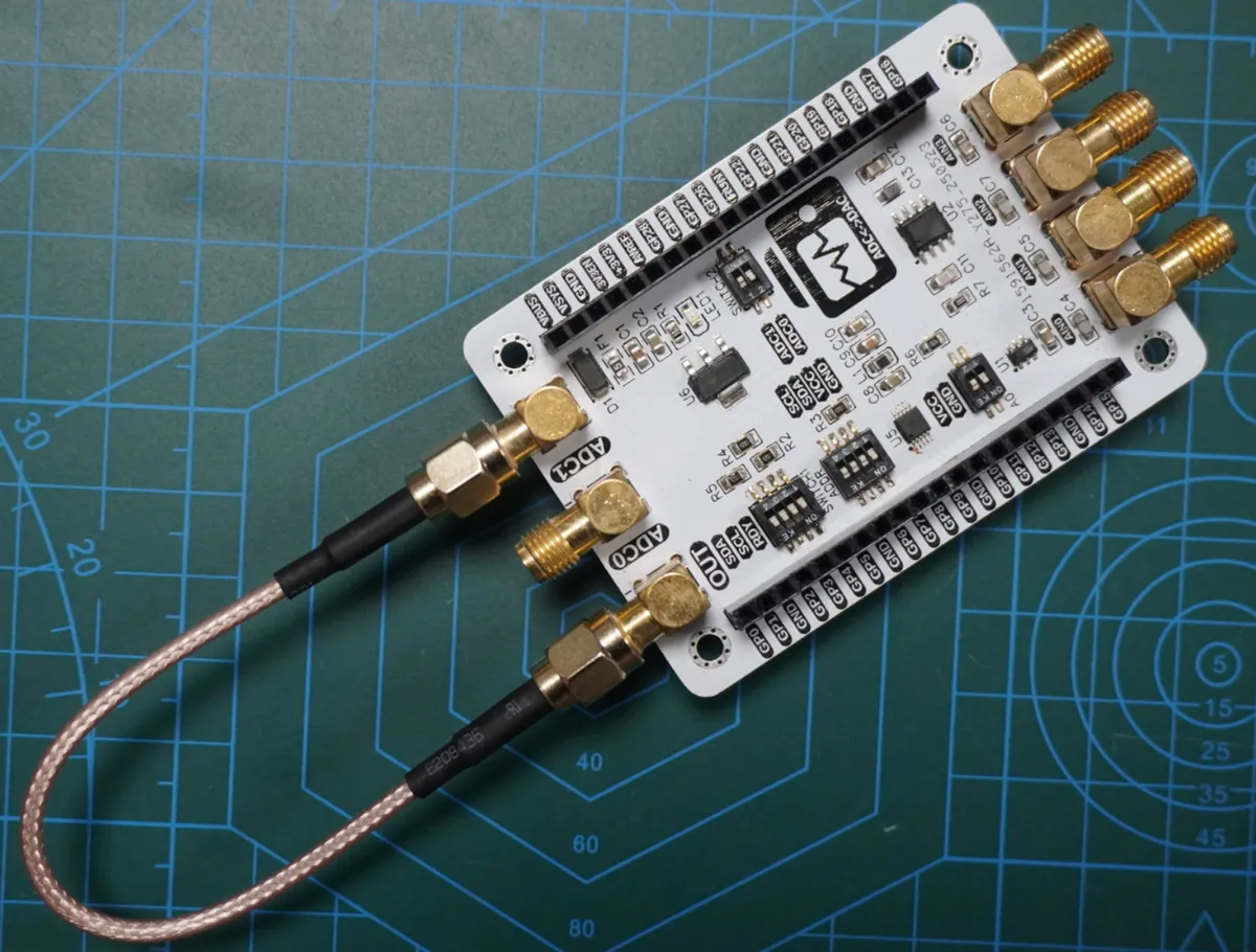
The following code can be found in the material package we provide, in the elegance-devkit v1\Demo\62 DAC_Sin folder.
In the following code, we generate a sine wave signal via an external DAC (MCP4725), read the voltage value through the ADC, and meanwhile send the voltage value via the serial port.
The sample code is shown below:
# Python env   : MicroPython v1.23.0
# -*- coding: utf-8 -*-
# @Time    : 2024/9/1 2:10 PM
# @Author  : Li Qingshui
# @File    : main.py
# @Description : DAC experiment, using an external DAC chip to generate a sine waveform

# ======================================== Import Modules ========================================

# Import the hardware module
from machine import ADC, Timer, Pin, I2C, UART
# Import time-related modules
import time
# Import the module for accessing and controlling MicroPython internals
import micropython
# Import the math library for calculating the sine wave
import math
# Import the mcp4725 module to control the DAC chip
from mcp4725 import MCP4725

# ======================================== Global Variables ============================================

# mcp4725 chip address
DAC_ADDRESS = 0x00
# Voltage conversion factor
adc_conversion_factor = 3.3 / (65535)

# ======================================== Functions ============================================

# Timer callback function
def timer_callback(timer: Timer) -> None:
    """
    Timer callback function, used to read ADC data periodically and call the user-defined callback function.

    Args:
        timer (machine.Timer): Timer instance.

    Returns:
        None
    """

    # Declare global variables
    global adc,adc_conversion_factor

    # Read ADC data
    value = adc.read_u16() * adc_conversion_factor
    # Call the user-defined callback function
    micropython.schedule(user_callback, (value))

# User-defined callback function
def user_callback(value: float) -> None:
    """
    User-defined callback function, used to process the voltage value sampled by the ADC and send it over the serial port.

    Args:
        value (float): Voltage value sampled by the ADC.

    Returns:
        None
    """
    # Declare global variables
    global uart

    # Get the floating-point number and round it to two decimal places
    formatted_value = "{:.2f}".format(value)
    # Send the sampled voltage data over the serial port
    uart.write(str(formatted_value) + '\r\n')
    # Print the sampled voltage data to the terminal
    print('dac generated voltage: ' + str(formatted_value))

# ======================================== Custom Classes ============================================

# ======================================== Initialization ==========================================

# Delay 3 s to wait for the device to finish powering up
time.sleep(3)
# Print debug information
print("FreakStudio : Using DAC to generate sine wave")

# Create a hardware I2C instance using the I2C1 peripheral, with a clock frequency of 400KHz, SDA pin 2, and SCL pin 3
i2c = I2C(id=1, sda=Pin(2), scl=Pin(3), freq=400000)

# Start scanning for devices on the I2C bus and return a list of slave addresses
devices_list = i2c.scan()
print('START I2C SCANNER')

# If devices_list is empty, no device is connected to the I2C bus
if len(devices_list) == 0:
    print("No i2c device !")
# If not empty, print the slave device addresses
else:
    print('i2c devices found:', len(devices_list))
    # Iterate over the slave device address list
    for device in devices_list:
        # If the device address is between 0x60 and 0x61, it is a DAC chip
        if 0x60 <= device <= 0x61:
            print("I2C hexadecimal address: ", hex(device))
            DAC_ADDRESS = device

# Create the DAC object, using the I2C0 peripheral, with address DAC_ADDRESS
dac = MCP4725(i2c, DAC_ADDRESS)
# Read the DAC configuration information
eeprom_write_busy, power_down, value, eeprom_power_down, eeprom_value = dac.read()
print(eeprom_write_busy, power_down, value, eeprom_power_down, eeprom_value)
# Configure the DAC: cancel power-down mode, output voltage 0V, write to EEPROM
dac.config(power_down='Off',value=0,eeprom=True)
# Delay 50ms; reading immediately after configuration causes an error
time.sleep_ms(50)
# Read the DAC configuration information
eeprom_write_busy, power_down, value, eeprom_power_down, eeprom_value = dac.read()
print(eeprom_write_busy, power_down, value, eeprom_power_down, eeprom_value)

# Create the ADC instance: ADC1-GP27
adc = ADC(1)
# Create a software timer object
timer = Timer(-1)
# Start the timer, triggering the timer_callback function every 5ms to sample voltage with the ADC
timer.init(period=5, mode=Timer.PERIODIC, callback=timer_callback)

# Create the serial port object, set the baud rate to 115200
uart = UART(0, 115200)
# Initialize the uart object with a baud rate of 115200, 8 data bits, no parity bit, and 1 stop bit
# Set the serial port timeout to 100ms
uart.init(baudrate  = 115200,
          bits      = 8,
          parity    = None,
          stop      = 1,
          tx        = 0,
          rx        = 1,
          timeout   = 100)

# ========================================  Main Program  ===========================================

# Generate the sine wave
for i in range(10000):
    # Calculate the voltage value of the sine wave
    value = 3.3 * math.sin(2 * math.pi * i / 100) + 3.3
    # Convert the voltage value of the sine wave to an integer
    value = int(value * 4095 / 6.6)
    # Write the analog value to the DAC
    dac.write(value)
    # Delay 10ms
    time.sleep_ms(10)

# Stop ADC sampling
timer.deinit()
In the above code, we have completed the following tasks:
- Delay for 3 seconds and wait for the device to power on.
- Create an I2C instance and scan the devices on the I2C bus to determine the DAC address.
- Create and configure an MCP4725 DAC instance, including reading and setting the DAC configuration.
- Create an ADC instance, configure a timer for periodically reading ADC data, and configure a serial port for data transmission; in the timer callback function, we read the ADC data and process it via the
user_callbackfunction, and in the user-defined callback function, format the voltage value read from the ADC to two decimal places and send the data through the serial port.
In the main function section, we have completed the following work:
- Generate a sine wave signal in the main program and output it to the DAC to control the frequency and amplitude of the output.
- After the completion signal is generated, stop the timer to halt the ADC acquisition.
The overall operation Sequence Diagram is shown as follows:
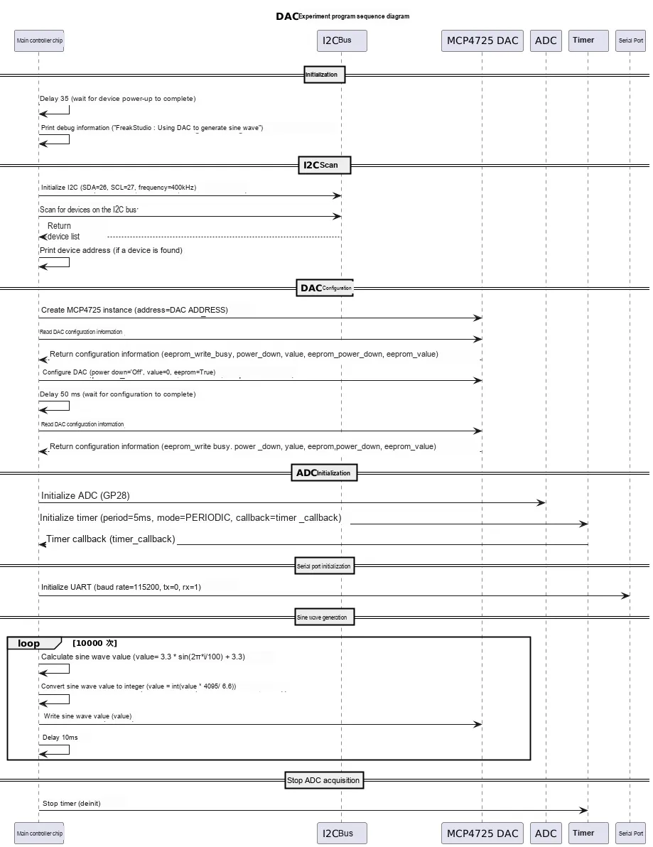
Open the SerialPlot software, select the corresponding port connected to the USB-to-TTL chip, and click the Open button:

Data Format Selection ASCII encoding, with other configurations left as default:
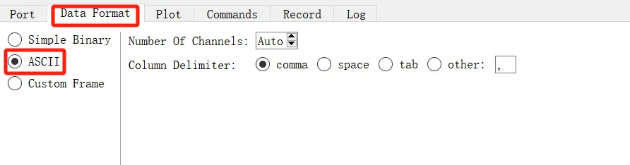
3.1 Application Experiment - PC Software Configuration.mp4 627 KB
Burn the code, open the terminal, and the output is as follows:
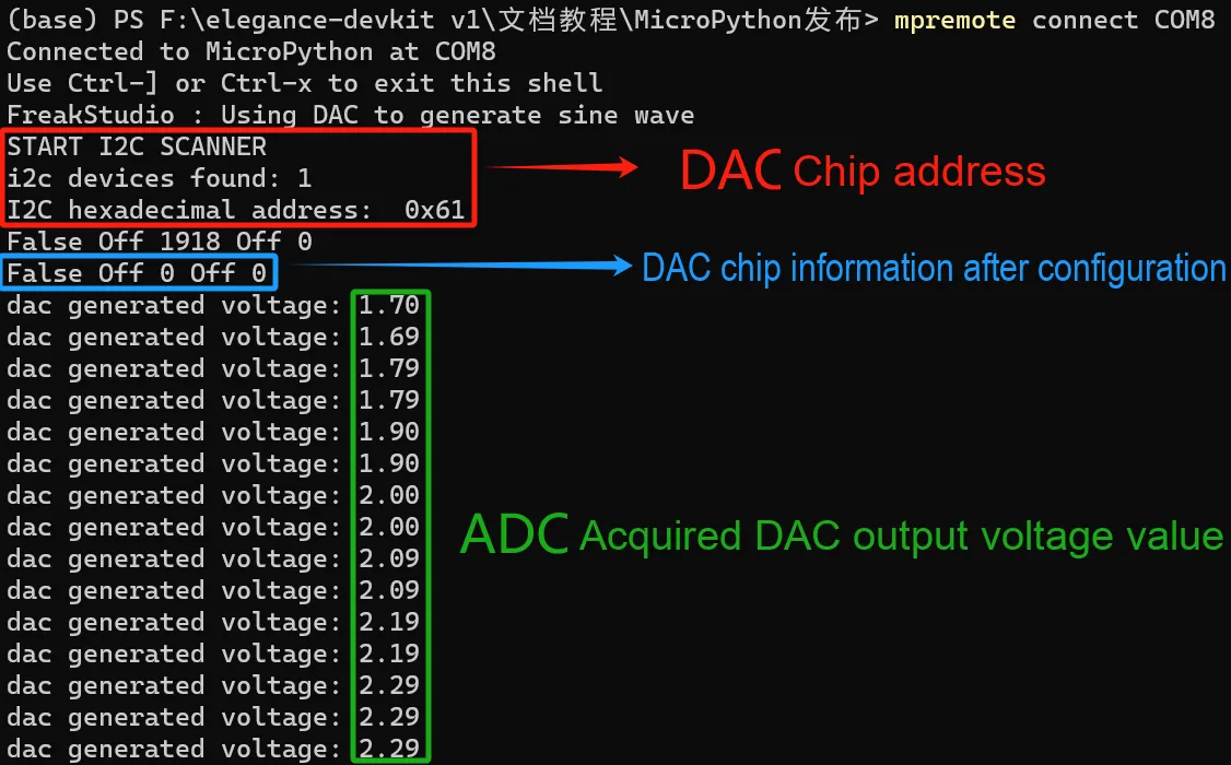
As can be seen, the DAC chip MCP4725 has an address of 0x60, and the configuration and method of the DAC chip work properly.
Open SerialPlot software, and you can see that the displayed DAC output voltage is a sine curve.
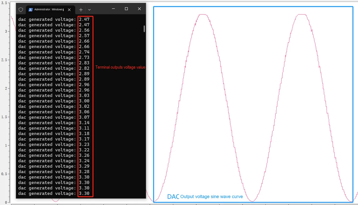
3.1 Application Experiment.mp4 29.0 MB
3.2 Implementing a Waveform Generator with the MCP4725
In the following code, we use the DAC chip MCP4725 on the Raspberry Pi Pico to generate different waveform signals, and output the waveform voltage values collected by the ADC via the serial port. The wiring of components is the same as in the previous section:
Raspberry Pi Pico Pinout | Interface Type | Connected External Devices / Applications | Key Parameters / Description |
GP2 | I2C | SDA line of the DAC chip (MCP4725) | Belongs to the I2C1 peripheral, with a communication frequency of 400 KHz |
GP3 | I2C | The SCL line of the DAC chip (MCP4725) | Belongs to the I2C1 peripheral, with a communication frequency of 400 KHz and a device address range of 0x60-0x61 |
GP27 | ADC | Voltage Acquisition Input Terminal | Corresponds to the ADC1 channel, and cooperates with the timer to trigger acquisition once every 5ms |
GP0 | UART | TX (transmit) line of serial communication | belongs to the UART0 peripheral, with a baud rate of 115200,8 data bits, no parity bit, and 1 stop bit |
GP1 | UART | RX (receive) line for serial communication | It belongs to the UART0 peripheral, with a baud rate of 115200 and a timeout period of 100ms |
The following code can be found in the elegance-devkit v1\Demo\63 DAC_WaveformGenerator folder of the resource package we provide.
The sample code is shown below:
# Python env   : MicroPython v1.23.0
# -*- coding: utf-8 -*-
# @Time    : 2024/9/1 2:10 PM
# @Author  : Li Qingshui
# @File    : main.py
# @Description : DAC experiment, using an external DAC chip to generate different waveforms

# ======================================== Import Modules ========================================

# Import the hardware module
from machine import ADC, Timer, Pin, I2C, UART
# Import time-related modules
import time
# Import the module for accessing and controlling MicroPython internals
import micropython
# Import the math library for calculating the sine wave
import math
# Import the mcp4725 module to control the DAC chip
from mcp4725 import MCP4725

# ======================================== Global Variables ============================================

# mcp4725 chip address
DAC_ADDRESS = 0x00
# Voltage conversion factor
adc_conversion_factor = 3.3 / (65535)

# ======================================== Functions ============================================

def timer_callback(timer: Timer) -> None:
    """
    Timer callback function, used to read ADC data periodically and call the user-defined callback function.

    Args:
        timer (machine.Timer): Timer instance.

    Returns:
        None: This function has no return value.

    Raises:
        None: This function does not raise exceptions.
    """

    # Declare global variables
    global adc,adc_conversion_factor

    # Read ADC data
    value = adc.read_u16() * adc_conversion_factor
    # Call the user-defined callback function
    micropython.schedule(user_callback, (value))

def user_callback(value: float) -> None:
    """
    User-defined callback function, used to process the voltage value sampled by the ADC and send it over the serial port.

    Args:
        value (float): Voltage value sampled by the ADC.

    Returns:
        None: This function has no return value.

    Raises:
        None: This function does not raise exceptions.
    """
    # Declare global variables
    global uart

    # Get the floating-point number and round it to two decimal places
    formatted_value = "{:.2f}".format(value)
    # Send the sampled voltage data over the serial port
    uart.write(str(formatted_value) + '\r\n')

# ======================================== Custom Classes ============================================

# Waveform generator class, used to generate voltage signals of different waveforms
class WaveformGenerator:
    """
    Waveform generator class, used to generate voltage signals of different waveforms.

    This class uses a DAC chip (such as the MCP4725) to generate sine, square and triangle wave signals, and supports setting parameters such as frequency, amplitude and DC offset.
    The waveform data is output to the DAC periodically by a timer, thus achieving continuous waveform generation.

    Attributes:
        dac (MCP4725): DAC chip instance, used to generate the waveform signal.
        frequency (float): Signal frequency, in Hz.
        amplitude (float): Signal amplitude, in V.
        offset (float): DC offset, in V.
        waveform (str): Waveform type, supports 'sine' (sine wave), 'square' (square wave) and 'triangle' (triangle wave).
        rise_ratio (float): Rising slope of the triangle wave, in the range 0 to 1.
        sample_rate (int): Sampling rate, fixed at 50 sample points.
        dac_resolution (int): Resolution of the DAC; for a 12-bit DAC the range is 0 to 4095.
        samples (list[int]): List of generated sample point data.
        index (int): Current sample point index, used to output the waveform data step by step.
        timer (Timer): Timer instance, used to trigger the waveform output periodically.

    Methods:
        __init__(dac, frequency=1, amplitude=1.65, offset=1.65, waveform='sine', rise_ratio=0.5):
            Initialize the waveform generator instance.
        generate_samples() -> list[int]:
            Generate sample point data according to the waveform type.
        update(t: Timer) -> None:
            Timer callback function, used to output the data of the next sample point.
        start() -> None:
            Start the waveform generator.
        stop() -> None:
            Stop the waveform generator.
    """
    def __init__(self, dac: 'MCP4725', frequency: float = 1, amplitude: float = 1.65, offset: float = 1.65,
                 waveform: str = 'sine', rise_ratio: float = 0.5) -> None:
        """
        Initialize the waveform generator instance.

        This method initializes the basic settings of the waveform generator, including the DAC object, signal frequency, amplitude, offset, waveform type and the rising slope of the triangle wave.

        Args:
            dac (MCP4725): DAC chip instance, used to generate the waveform signal.
            frequency (float, optional): Signal frequency, default 1 Hz. Must be greater than 0 and less than or equal to 10 Hz.
            amplitude (float, optional): Signal amplitude, default 1.65V. Must be between 0 and 3.3V.
            offset (float, optional): DC offset, default 1.65V. Must be between 0 and 3.3V.
            waveform (str, optional): Waveform type, which can be 'sine' (sine wave), 'square' (square wave) or 'triangle' (triangle wave), default 'sine'.
            rise_ratio (float, optional): Rising slope of the triangle wave, default 0.5; the value must be between 0 and 1.

        Returns:
            None: This method has no return value.

        Raises:
            ValueError: Raised if the passed parameters are outside the predefined ranges.
        """

        # Parameter input check
        # Parameter input check, ensure the frequency is between 0 and 10 Hz
        if not (0 < frequency <= 10):
            raise ValueError("Frequency must be between 0 and 10 Hz.")
        # Check whether the amplitude is between 0 and 3.3V
        if not (0 <= amplitude <= 3.3):
            raise ValueError("Amplitude must be between 0 and 3.3V.")
        # Check whether the DC offset is between 0 and 3.3V
        if not (0 <= offset <= 3.3):
            raise ValueError("Offset must be between 0 and 3.3V.")
        # Ensure the sum of amplitude and offset does not exceed 3.3V, to prevent the output from exceeding the DAC range
        if not(0 <= amplitude+offset <= 3.3):
            raise ValueError("Amplitude + offset must be between 0 and 3.3V.")
        # Check whether the waveform type is sine, square or triangle
        if waveform not in ['sine', 'square', 'triangle']:
            raise ValueError("Waveform must be 'sine', 'square', or 'triangle'.")
        # Check whether the rising-edge ratio of the triangle wave is between 0 and 1
        if not (0 <= rise_ratio <= 1):
            raise ValueError("Rise ratio must be between 0 and 1.")

        # Save the DAC object
        self.dac = dac

        # Initialize the timer object; -1 means it is not bound to any hardware timer at initialization
        self.timer = Timer(-1)

        # Save the waveform generator parameters
        # Signal frequency
        self.frequency = frequency
        # Signal amplitude
        self.amplitude = amplitude
        # DC offset
        self.offset = offset
        # Waveform type
        self.waveform = waveform
        # Rising-edge ratio of the triangle wave
        self.rise_ratio = rise_ratio

        # Fixed 50 sample points; the number of sample points of the discrete signal
        self.sample_rate = 50

        # Resolution of the 12-bit DAC, meaning the DAC output range is 0 to 4095
        self.dac_resolution = 4095

        # Generate sample point data according to the waveform type
        self.samples = self.generate_samples()

        # Initialize the current sample point index, used to output waveform data step by step
        self.index = 0

    def generate_samples(self) -> list[int]:
        """
        Generate sample point data according to the waveform type.

        This method generates the corresponding sample point data according to the selected waveform type (sine wave, square wave, triangle wave) and converts each sample point to a value acceptable to the DAC.

        Returns:
            list[int]: List of sample points converted to DAC values.

        Raises:
            None: This method does not raise exceptions.
        """

        # Function that converts a voltage value to a DAC value
        def to_dac_value(voltage):
            # Calculate the corresponding DAC output value from the voltage value; the DAC resolution is 4095 and the voltage range is 0 to 3.3V
            return int(voltage / 3.3 * self.dac_resolution)

        # Initialize a list to store the generated sample point data
        samples = []

        # Generate sample point data according to the selected waveform
        if self.waveform == 'sine':
            # Sine wave: generate the corresponding voltage value from the angle
            for i in range(self.sample_rate):
                # Calculate the angle corresponding to the current sample point; the angle has a period of 2π
                angle = 2 * math.pi * i / self.sample_rate
                # Calculate the voltage value of the current sample point using the sine function
                voltage = self.offset + self.amplitude * math.sin(angle)
                # Convert the voltage value to the corresponding DAC value and add it to the sample list
                samples.append(to_dac_value(voltage))

        elif self.waveform == 'square':
            # Square wave: generate alternating high and low voltage values according to the sample point index
            for i in range(self.sample_rate):
                # The voltage is high in the first half of the period and low in the second half
                if i < self.sample_rate // 2:
                    # High level
                    voltage = self.offset + self.amplitude
                else:
                    # Low level
                    voltage = self.offset - self.amplitude
                # Convert the voltage value to the corresponding DAC value and add it to the sample list
                samples.append(to_dac_value(voltage))

        elif self.waveform == 'triangle':
            # Triangle wave: generate voltage values from the rising and falling edges
            for i in range(self.sample_rate):
                if i < self.sample_rate * self.rise_ratio:
                    # Rising edge: the voltage rises from offset - amplitude to offset + amplitude
                    voltage = self.offset + 2 * self.amplitude * (
                            i / (self.sample_rate * self.rise_ratio)) - self.amplitude
                else:
                    # Falling edge: the voltage falls from offset + amplitude to offset - amplitude
                    voltage = self.offset + 2 * self.amplitude * (
                            (self.sample_rate - i) / (self.sample_rate * (1 - self.rise_ratio))) - self.amplitude
                # Convert the voltage value to the corresponding DAC value and add it to the sample list
                samples.append(to_dac_value(voltage))

        # Return the list of generated sample point data
        return samples

    def update(self, t: Timer) -> None:
        """
        Timer callback function, called on a timer interrupt, used to output the data of the next sample point.

        This method is called on a timer interrupt. Each time it is called, it writes the data of the current sample point to the DAC and updates the index to point to the next sample point.

        Args:
            t (Timer): Timer object, representing the timer that triggered the callback.

        Returns:
            None: This method has no return value.

        Raises:
            None: This method does not raise exceptions.
        """

        # Write the data of the current sample point to the DAC to generate the corresponding voltage output
        self.dac.write(self.samples[self.index])
        # Update the sample point index to point to the next sample point
        self.index = (self.index + 1) % self.sample_rate

    def start(self) -> None:
        """
        Start the waveform generator and the timer, periodically generating and outputting waveform data.

        This method starts the timer and calls the callback function on each period trigger, outputting waveform data at the preset frequency.

        Args:
            None: This method does not accept any parameters.

        Returns:
            None: This method has no return value.

        Raises:
            None: This method does not raise exceptions.
        """

        # Initialize the timer to trigger timer interrupts at frequency freq*self.sample_rate
        self.timer.init(freq=self.frequency * self.sample_rate, mode=Timer.PERIODIC, callback=self.update)

    def stop(self) -> None:
        """
        Stop the waveform generator, stop the timer, and stop the output of waveform data.

        This method stops the timer, and the waveform output will pause.

        Args:
            None: This method does not accept any parameters.

        Returns:
            None: This method has no return value.

        Raises:
            None: This method does not raise exceptions.
        """

        # Stop the timer and release the interrupt
        self.timer.deinit()
        # Reset the sample point index to 0 to ensure the next start begins from the first sample point
        self.index = 0

# ======================================== Initialization ==========================================

# Delay 3 s to wait for the device to finish powering up
time.sleep(3)
# Print debug information
print("FreakStudio : Using DAC to generate differential waveform")

# Create a hardware I2C instance using the I2C1 peripheral, with a clock frequency of 400KHz, SDA pin 2, and SCL pin 3
i2c = I2C(id=1, sda=Pin(2), scl=Pin(3), freq=400000)

# Start scanning for devices on the I2C bus and return a list of slave addresses
devices_list = i2c.scan()
print('START I2C SCANNER')

# If devices_list is empty, no device is connected to the I2C bus
if len(devices_list) == 0:
    print("No i2c device !")
# If not empty, print the slave device addresses
else:
    print('i2c devices found:', len(devices_list))
    # Iterate over the slave device address list
    for device in devices_list:
        # If the device address is between 0x60 and 0x61, it is a DAC chip
        if 0x60 <= device <= 0x61:
            print("I2C hexadecimal address: ", hex(device))
            DAC_ADDRESS = device

# Create the DAC object, using the I2C0 peripheral, with address DAC_ADDRESS
dac = MCP4725(i2c, DAC_ADDRESS)
# Read the DAC configuration information
eeprom_write_busy, power_down, value, eeprom_power_down, eeprom_value = dac.read()
print(eeprom_write_busy, power_down, value, eeprom_power_down, eeprom_value)
# Configure the DAC: cancel power-down mode, output voltage 0V, write to EEPROM
dac.config(power_down='Off',value=0,eeprom=True)
# Delay 50ms; reading immediately after configuration causes an error
time.sleep_ms(50)
# Read the DAC configuration information
eeprom_write_busy, power_down, value, eeprom_power_down, eeprom_value = dac.read()
print(eeprom_write_busy, power_down, value, eeprom_power_down, eeprom_value)

# Create the serial port object, set the baud rate to 115200
uart = UART(0, 115200)
# Initialize the uart object with a baud rate of 115200, 8 data bits, no parity bit, and 1 stop bit
# Set the serial port timeout to 100ms
uart.init(baudrate  = 115200,
          bits      = 8,
          parity    = None,
          stop      = 1,
          tx        = 0,
          rx        = 1,
          timeout   = 100)

# Create the ADC instance: ADC1-GP27
adc = ADC(1)
# Create a software timer object
timer = Timer(-1)
# Start the timer, triggering the timer_callback function every 1ms; the ADC samples the voltage
timer.init(period=1, mode=Timer.PERIODIC, callback=timer_callback)

# ========================================  Main Program  ===========================================

# Generate the sine wave
print("FreakStudio : Generate Sine Waveform : 10Hz, 1.5V, 1.5V")
# Initialize the waveform generator
wave = WaveformGenerator(dac, frequency=10, amplitude=1.5, offset=1.5, waveform='sine')
# Start waveform generation
wave.start()
# Stop generation after running for a while
time.sleep(5)
wave.stop()

# Generate square wave
print("FreakStudio : Generate Square Waveform : 10Hz, 1.5V, 1.5V")
# Initialize the waveform generator
wave = WaveformGenerator(dac, frequency=10, amplitude=1.5, offset=1.5, waveform='square')
# Start waveform generation
wave.start()
# Stop generation after running for a while
time.sleep(5)
wave.stop()

# Generate triangle wave
print("FreakStudio : Generate Triangle Waveform : 10Hz, 1.5V, 1.5V, 0.8")
# Initialize the waveform generator
wave = WaveformGenerator(dac, frequency=10, amplitude=1.5, offset=1.5, waveform='triangle', rise_ratio=0.8)
# Start waveform generation
wave.start()
# Stop generation after running for a while
time.sleep(5)
wave.stop()

# Stop ADC sampling
timer.deinit()
Here, we have defined a custom WaveformGenerator class that implements square, sine, and triangular waves with adjustable frequency and amplitude, and outputs these signals to a DAC (Digital-to-Analog Converter):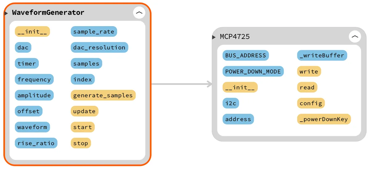
- First, validate the input parameters (frequency, amplitude, offset, waveform type, etc.) in the constructor to ensure they fall within a reasonable range, save the DAC object and waveform parameters, initialize the timer, and call the
generate_samplesmethod according to the input waveform parameters to generate sampling point data;
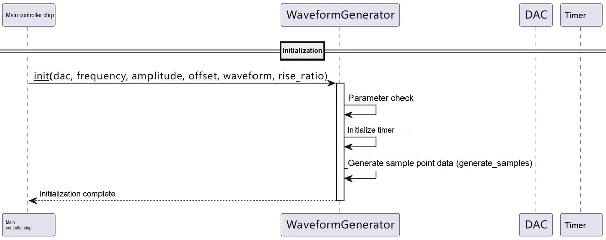
- In the
generate_samplesmethod, we generate corresponding sampling point data according to the waveform type:- Sine wave: Use the
math.sinfunction to generate sine wave data. - Square wave: Generate data with alternating high and low levels based on the sequence number of sampling points.
- Triangular wave: Generate linearly varying data based on the rising edge and falling edge.
Then return the generated list of sampling point data.
- Sine wave: Use the
- In the timer callback function (
updatemethod), write the data of the current sampling point to the DAC and update the sampling point index to point to the next sampling point (reuse the sampling point data in a loop).
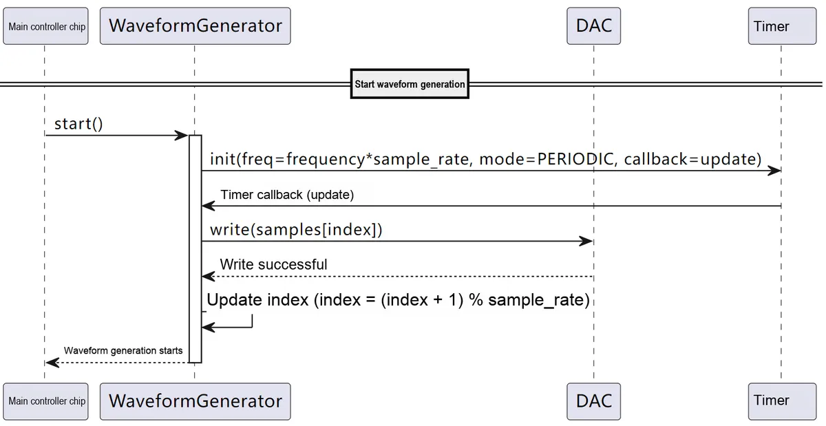
- After creating an instance of the
WaveformGeneratorclass, we initialize the timer via thestartmethod with a frequency ofself.frequency * self.sample_rateto periodically invoke theupdatemethod; once waveform generation is no longer required, thestopmethod can be called to halt the timer and reset the sample point index to 0.
Fundamentals of Digital Signals
In the above code, we define two parameters: the sampling rate sample_rate and the signal frequency frequency, which are specified as follows:
- Sample Rate: The sample rate of a signal refers to the number of samples collected per second. In this code,
sample_rateis fixed at 50, which means that when generating a signal, the waveform is divided into 50 discrete points to approximate a continuous waveform; a higher sample rate can reproduce the waveform more accurately, but it will also increase the processing burden - Signal Frequency and Sampling Rate: The signal frequency refers to the number of complete waveforms generated per second; here, the timer frequency is set to
frequency * sample_rate, which means the DAC will update 50 times during each cycle.
When the signal frequency is 1 Hz, the timer frequency will be set to 50 Hz, which ensures that one complete waveform cycle is generated per second, and each waveform contains 50 sampling points.
In the main program, we sequentially create 3 WaveformGenerator instances to generate a sine wave, a square wave and a triangular wave. The rise edge ratio of the triangular wave is set to 0.8, all three waveforms will stop generating after 5 seconds, and the timer will be turned off and ADC acquisition will be stopped after all three waveforms are fully generated.
The overall Sequence Diagram of the program is shown below:
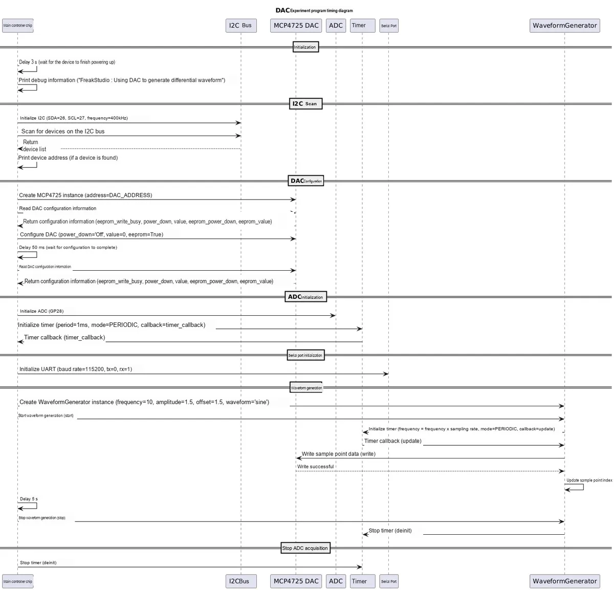
Open SerialPlot software, select the corresponding port connected to the USB-to-TTL chip, and click the Open button:

Data Format Selection ASCII encoding, with other configurations left as default:
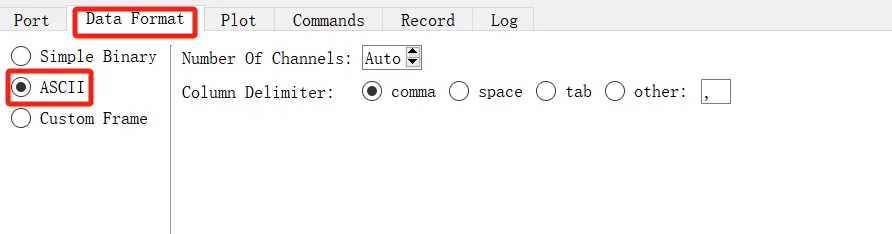
3.1 Application Experiment - PC Software Configuration.mp4 627 KB
Burn the code, open the terminal, and the output is as follows:
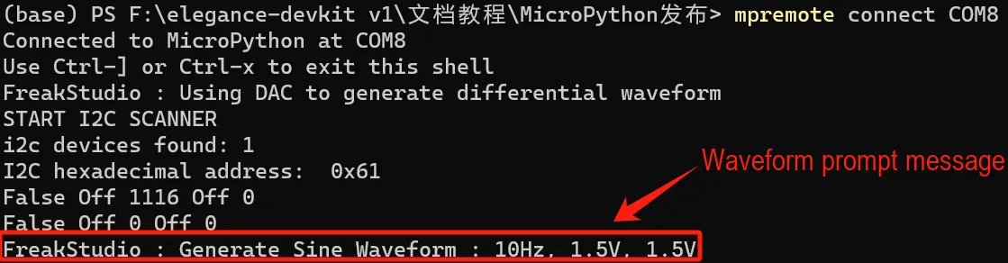
Open the SerialPlot software, and you will see that both the frequency and amplitude of the displayed DAC output voltage are normal:
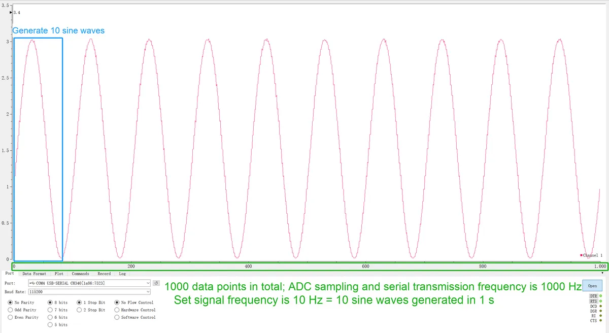
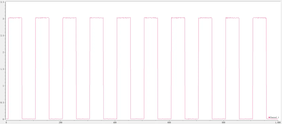
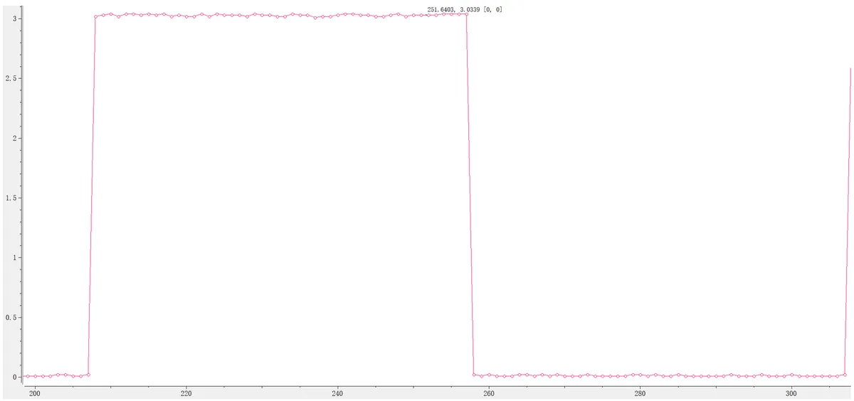
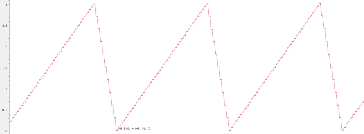
3.2 Application Experiment.mp4 53.5 MB
Compared with DDS signal generators, using the MCP4725 DAC to generate waveforms requires calculating each point of the waveform in the microcontroller via software and then sending them to the DAC point by point, which not only increases system complexity but also consumes more processing resources (sending is timed via a timer; frequent timer interrupts will be generated when the frequency of the signal to be sent is high, and more memory will be occupied when the number of sampling points of the required waveform is large). Meanwhile, the frequency of the waveform completely depends on the speed at which the microcontroller updates the DAC values, and its frequency accuracy and resolution are limited by the clock of the microcontroller and the timer resolution, making it difficult to achieve extremely high-precision frequency control. The maximum frequency updated by using a software timer in MicroPython is 1000Hz, which greatly limits the frequency range of the generated signal.
Moreover, when using MCP4725 , due to data transmission through the I2C bus, data transmission may be affected by I2C bus blockage or other tasks of the microcontroller, resulting in jitter or instability in the output of the waveform generator. Therefore, in practical applications, we often use external DDS signal generation chips to implement waveform generation functions.
3.3 Implementation of Waveform Generator Based on DS3502
Here, we first need to insert the Fengya No. 1 Board - Grove Interface Expansion Board into the Fengya No. 1 Board - Universal Compatible Expansion Board, and meanwhile use a HY2.0-4P cable to connect the I2C1 port on the Fengya No. 1 Board - Grove Interface Expansion Board with the I2C port on the GraftSense - DS3502-based Digital Potentiometer Module:
Then insert the Fengya No.1 Board-Universal Compatible Expansion Board into the Fengya No.1 Board-Data Conversion Board , and open the SCL , SDA and RDY options of the Fengya No.1 Board-Data Conversion Board on the SWITCH1 DIP switch, and open the ADC1 switch option of the SWITCH2 DIP switch:
Then, on the back side of the GraftSense - DS3502-based Digital Potentiometer Module, configure the device address by shorting the three pads of the address selection pins A0 and A1 to GND or VCC; in addition, turn on the SW1 DIP switch's RL to short it to GND, turn on its V+ to short it to RH, and connect a + 5V power supply to the U3 terminal's RL and V+ pins (it is recommended to use the GraftSense - LM2596S-based Adjustable Power Supply Module):
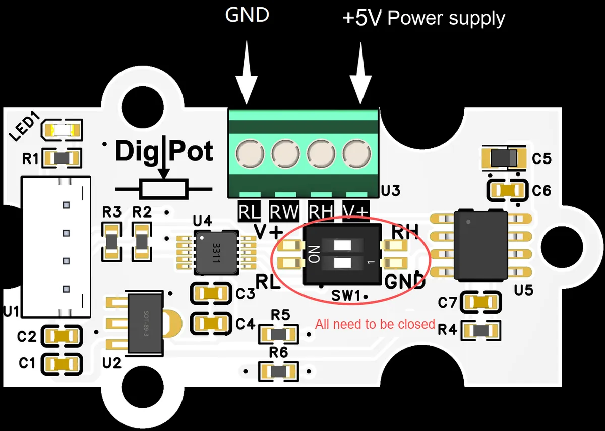
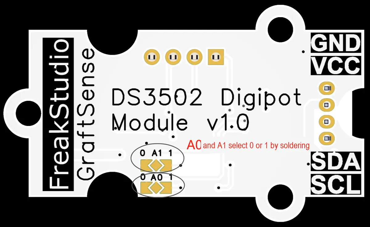
The physical image after insertion is as follows:
In addition, we first need to connect the MiniUSB data cable to the serial port on Fengya No. 1 Board - Universal Compatible Expansion Board. Here, GP0 and GP1 are the default pins of the hardware serial port UART0 of the Raspberry Pi Pico:
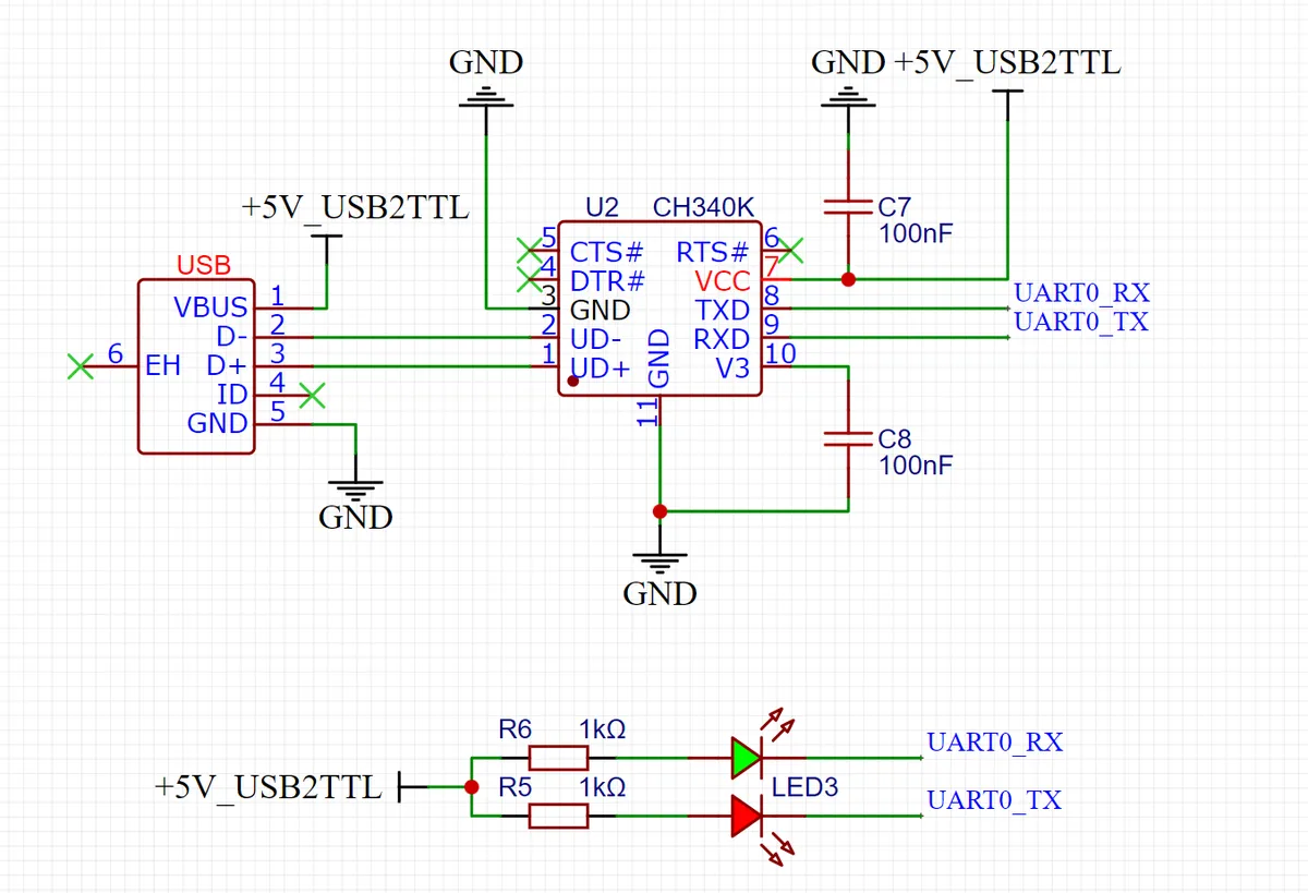
Here, the GraftSense - DS3502-based digital potentiometer module has its signal output terminal on U3, which is the RW pin. We also need to use an SMA to DuPont wire adapter to connect the GraftSense - DS3502-based digital potentiometer module 's terminal on U3, i. e., the RW signal output interface, to the Fengya No. 1 Board - Data Conversion Board ' s ADC0 internal analog-to-digital conversion SMA interface, as shown in the following figure:
The overall connection diagram is shown as follows:
The wiring conditions of the components are shown in the following table:
| Module / Device | Pin / Interface / Configuration item | Connection target | Target pin / Interface |
| Raspberry Pi Pico (core of the Fengya No. 1 board) | GP10 (I2C1_SDA) | Grove interface expansion board I2C1 | SDA pin |
| Raspberry Pi Pico (core of the Fengya No. 1 board) | GP11 (I2C1_SCL) | Grove interface expansion board I2C1 | SCL pin |
| Grove interface expansion board | I2C1_SDA | DS3502 module I2C | SDA interface |
| Grove interface expansion board | I2C1_SCL | DS3502 module I2C | SCL interface |
| DS3502 module | Address select pin A0 | GND/VCC | Pad shorted |
| DS3502 module | Address select pin A1 | GND/VCC | Pad shorted |
| DS3502 module | SW1 DIP switch RL | Module internal GND | DIP switch shorted |
| DS3502 module | SW1 DIP switch V+ | Module internal RH | DIP switch shorted |
| 3.3V power supply | Output terminal | DS3502 module U3 terminal | RL interface |
| 3.3V power supply | Output terminal | DS3502 module U3 terminal | V+ interface |
| Raspberry Pi Pico (core of the Fengya No. 1 board) | GP0 (UART0_TX) | Universal compatible expansion board serial port | TX pin |
| Raspberry Pi Pico (core of the Fengya No. 1 board) | GP1 (UART0_RX) | Universal compatible expansion board serial port | RX pin |
| Universal compatible expansion board | Serial port interface | MiniUSB cable | USB male end |
| DS3502 module | U3 terminal RW (signal output) | Data conversion board ADC0 | SMA interface |
| Data conversion board | ADC0 interface | Raspberry Pi Pico (core of the Fengya No. 1 board) | GP26 (ADC0) |
The following code can be found in the elegance-devkit v1\Demo\64 DAC_Digipot folder in the resource package we provide.
In the following sample code, a digital potentiometer chip DS3502 is used on the Raspberry Pi Pico to generate different waveform signals, and the waveform voltage values acquired by ADC0 are output via the serial port.
First, we will move the waveform generation defined in the previous section WaveformGenerator class into a separate dac_waveformgenerator.py file, and make some modifications to it at the same time:
# Python env   : MicroPython v1.23.0
# -*- coding: utf-8 -*-
# @Time    : 2025/3/21 3:13 PM
# @Author  : Li Qingshui
# @File    : dac_waveformgenerator.py
# @Description : A class that uses the DS3502 chip to generate sine, triangle, and sawtooth waves
# This part of the code was developed by leeqingshui and is licensed under CC BY-NC 4.0

# ======================================== Import Modules =========================================

# Import the math library for calculating the sine wave
import math
# Import the hardware module
from machine import Timer
# Import the ds3502 module used to control the digital potentiometer chip
from ds3502 import DS3502

# ======================================== Global Variables ============================================

# ======================================== Functions ============================================

# ======================================== Custom Classes ============================================

class WaveformGenerator:
    def __init__(self, dac: 'DS3502', frequency: float = 1, amplitude: float = 1.65, offset: float = 1.65,
                 waveform: str = 'sine', rise_ratio: float = 0.5, vref: float = 3.3) -> None:
        """
        Initialize the waveform generator instance.

        This method initializes the basic settings of the waveform generator, including the DS3502 object, signal frequency, amplitude, offset, waveform type, rising slope of the triangle wave, and bias voltage.

        Args:
            dac (DS3502): DS3502 digital potentiometer instance, used to generate the waveform signal.
            frequency (float, optional): Signal frequency, default 1 Hz. Must be greater than 0 and less than or equal to 10 Hz.
            amplitude (float, optional): Signal amplitude, default 1.65V. Must be between 0 and vref.
            offset (float, optional): DC offset, default 1.65V. Must be between 0 and vref.
            waveform (str, optional): Waveform type, which can be 'sine' (sine wave), 'square' (square wave) or 'triangle' (triangle wave), default 'sine'.
            rise_ratio (float, optional): Rising slope of the triangle wave, default 0.5; the value must be between 0 and 1.
            vref (float, optional): Bias voltage, default 3.3V. Must be greater than 0.

        Returns:
            None: This method has no return value.

        Raises:
            ValueError: Raised if the passed parameters are outside the predefined ranges.
        """
        # Parameter input check
        if not (0 < frequency <= 10):
            raise ValueError("Frequency must be between 0 and 10 Hz.")
        if not (0 <= amplitude <= vref):
            raise ValueError(f"Amplitude must be between 0 and {vref}V.")
        if not (0 <= offset <= vref):
            raise ValueError(f"Offset must be between 0 and {vref}V.")
        if not (0 <= amplitude + offset <= vref):
            raise ValueError(f"Amplitude + offset must be between 0 and {vref}V.")
        if waveform not in ['sine', 'square', 'triangle']:
            raise ValueError("Waveform must be 'sine', 'square', or 'triangle'.")
        if not (0 <= rise_ratio <= 1):
            raise ValueError("Rise ratio must be between 0 and 1.")
        if vref <= 0:
            raise ValueError("Vref must be greater than 0.")

        # Save the DS3502 object
        self.dac = dac

        # Initialize the timer object
        self.timer = Timer(-1)

        # Save the waveform generator parameters
        self.frequency = frequency  # Signal frequency
        self.amplitude = amplitude  # Signal amplitude
        self.offset = offset  # DC offset
        self.waveform = waveform  # Waveform type
        self.rise_ratio = rise_ratio  # Rising-edge ratio of the triangle wave
        self.vref = vref  # Bias voltage

        # Fixed 50 sample points
        self.sample_rate = 50

        # The DS3502 has a 7-bit resolution (128 levels)
        self.dac_resolution = 127

        # Generate sample point data according to the waveform type
        self.samples = self.generate_samples()

        # Initialize the current sample point index
        self.index = 0

    def generate_samples(self) -> list[int]:
        """
        Generate sample point data according to the waveform type.

        Returns:
            list[int]: List of sample points converted to DS3502 values.
        """
        # Function that converts a voltage value to a DS3502 value
        def to_dac_value(voltage):
            # The DS3502 has a 7-bit resolution, and the voltage range is 0 to vref
            return int(voltage / self.vref * self.dac_resolution)

        # Initialize a list to store the generated sample point data
        samples = []

        # Generate sample point data according to the selected waveform
        if self.waveform == 'sine':
            # Sine wave
            for i in range(self.sample_rate):
                angle = 2 * math.pi * i / self.sample_rate
                voltage = self.offset + self.amplitude * math.sin(angle)
                samples.append(to_dac_value(voltage))

        elif self.waveform == 'square':
            # Square wave
            for i in range(self.sample_rate):
                if i < self.sample_rate // 2:
                    # High level
                    voltage = self.offset + self.amplitude
                else:
                    # Low level
                    voltage = self.offset - self.amplitude
                samples.append(to_dac_value(voltage))

        elif self.waveform == 'triangle':
            # Triangle wave
            for i in range(self.sample_rate):
                if i < self.sample_rate * self.rise_ratio:
                    voltage = self.offset + 2 * self.amplitude * (
                            i / (self.sample_rate * self.rise_ratio)) - self.amplitude
                else:
                    voltage = self.offset + 2 * self.amplitude * (
                            (self.sample_rate - i) / (self.sample_rate * (1 - self.rise_ratio))) - self.amplitude
                samples.append(to_dac_value(voltage))

        return samples

    def update(self, t: Timer) -> None:
        """
        Timer callback function, used to output the data of the next sample point.

        Args:
            t (Timer): Timer object.
        """
        # Write the data of the current sample point to the DS3502
        self.dac.write_wiper(self.samples[self.index])
        # Update the sample point index
        self.index = (self.index + 1) % self.sample_rate

    def start(self) -> None:
        """
        Start the waveform generator and the timer.
        """
        self.timer.init(freq=self.frequency * self.sample_rate, mode=Timer.PERIODIC, callback=self.update)

    def stop(self) -> None:
        """
        Stop the waveform generator and the timer.
        """
        self.timer.deinit()
        self.index = 0

# ======================================== Initialization ==========================================

# ========================================  Main Program  ===========================================
The modifications are as follows:
- In the initialization
__init__()method: take the bias voltage as one of the initialization parameters, so that users can dynamically set the bias voltage according to the actual hardware configuration (such as different power supply voltages) instead of hardcoding it as 3.3V; meanwhile, in the type annotation, modify the type of the input parameterdactoDS3502, and in the parameter check, ensure that the values ofamplitudeandoffsetdo not exceedvref, and add a check forvrefto ensure that it is greater than 0.
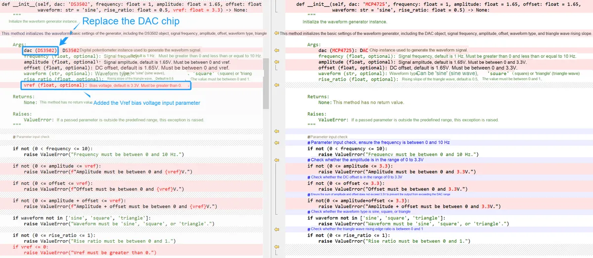
Meanwhile, change the attribute dac_resolution from 12 to 7:
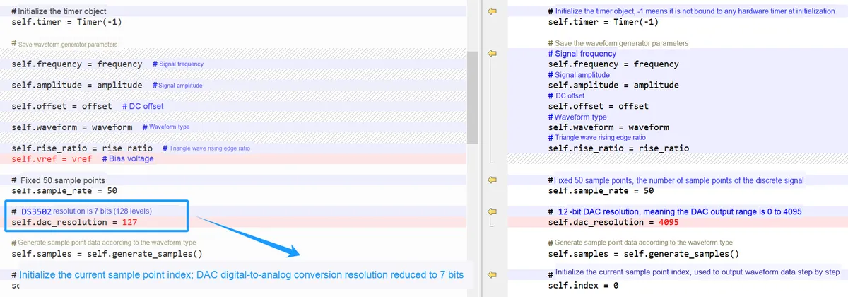
- In the generate sampling point data
generate_samples ()method:The resolution of DS3502is 7 bits (128 levels), not the 12 bits (4096 levels) ofMCP4725, so the generation logic of sampling points needs to be adjusted:

- In the timer callback
update ()function: modify thewritemethod towrite_wiperto adapt to theDS3502API:
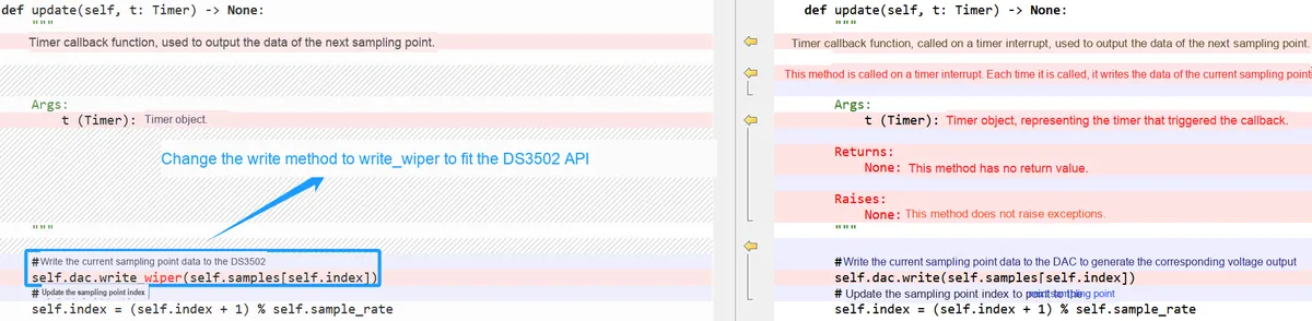
Sample code for the main program is shown below:
# Python env   : MicroPython v1.23.0
# -*- coding: utf-8 -*-
# @Time    : 2025/3/21 3:04 PM
# @Author  : Li Qingshui
# @File    : main.py
# @Description : Output arbitrary waveforms using the DS3502 digital potentiometer

# ======================================== Import Modules ========================================

# Import the hardware module
from machine import ADC, Timer, Pin, I2C, UART
# Import time-related modules
import time
# Import the module for accessing and controlling MicroPython internals
import micropython
# Import the math library for calculating the sine wave
import math
# Import the ds3502 module used to control the digital potentiometer chip
from ds3502 import DS3502
# Import the waveform generation module
from dac_waveformgenerator import WaveformGenerator

# ======================================== Global Variables ============================================

# DS3502 chip address
DAC_ADDRESS = 0x00
# Voltage conversion factor
adc_conversion_factor = 3.3 / (65535)

# ======================================== Functions ============================================

def timer_callback(timer: Timer) -> None:
    """
    Timer callback function, used to read ADC data periodically and call the user-defined callback function.

    Args:
        timer (machine.Timer): Timer instance.

    Returns:
        None: This function has no return value.

    Raises:
        None: This function does not raise exceptions.
    """

    # Declare global variables
    global adc, adc_conversion_factor

    # Read ADC data
    value = adc.read_u16() * adc_conversion_factor
    # Call the user-defined callback function
    micropython.schedule(user_callback, (value))

def user_callback(value: float) -> None:
    """
    User-defined callback function, used to process the voltage value sampled by the ADC and send it over the serial port.

    Args:
        value (float): Voltage value sampled by the ADC.

    Returns:
        None: This function has no return value.

    Raises:
        None: This function does not raise exceptions.
    """
    # Declare global variables
    global uart

    # Get the floating-point number and round it to two decimal places
    formatted_value = "{:.2f}".format(value)
    # Send the sampled voltage data over the serial port
    uart.write(str(formatted_value) + '\r\n')

# ======================================== Custom Classes ============================================

# ======================================== Initialization ==========================================

# Delay 3 s to wait for the device to finish powering up
time.sleep(3)
# Print debug information
print("FreakStudio : Using Digital Potentiometer chip DS3502 to generate differential waveform")

# Create a hardware I2C instance using the I2C1 peripheral, clock frequency 400KHz, SDA pin 10, SCL pin 11
i2c = I2C(id=1, sda=Pin(10), scl=Pin(11), freq=400000)

# Start scanning for devices on the I2C bus and return a list of slave addresses
devices_list = i2c.scan()
print('START I2C SCANNER')

# If devices_list is empty, no device is connected to the I2C bus
if len(devices_list) == 0:
    print("No i2c device !")
# If not empty, print the slave device addresses
else:
    print('i2c devices found:', len(devices_list))
    # Iterate over the slave device address list
    for device in devices_list:
        # If the device address is between 0x28 and 0x2B, it is a DS3502 chip
        if 0x28 <= device <= 0x2B:
            print("I2C hexadecimal address: ", hex(device))
            DAC_ADDRESS = device

# Create a DS3502 object using the I2C1 peripheral, with address DAC_ADDRESS
dac = DS3502(i2c, DAC_ADDRESS)
# Set the DS3502 to fast mode (write only to the WR register)
dac.set_mode(1)

# Create the serial port object, set the baud rate to 115200
uart = UART(0, 115200)
# Initialize the uart object with a baud rate of 115200, 8 data bits, no parity bit, and 1 stop bit
# Set the serial port timeout to 100ms
uart.init(baudrate=115200,
          bits=8,
          parity=None,
          stop=1,
          tx=0,
          rx=1,
          timeout=100)

# Create ADC instance: ADC0-GP26
adc = ADC(0)
# Create a software timer object
timer = Timer(-1)
# Start the timer, triggering the timer_callback function every 1ms; the ADC samples the voltage
timer.init(period=1, mode=Timer.PERIODIC, callback=timer_callback)

# ========================================  Main Program  ===========================================

# Generate the sine wave
print("FreakStudio : Generate Sine Waveform : 10Hz, 1.5V, 1.5V")
# Initialize the waveform generator
wave = WaveformGenerator(dac, frequency=5, amplitude=1.5, offset=1.5, waveform='sine', vref = 5)
# Start waveform generation
wave.start()
# Stop generation after running for a while
time.sleep(6)
wave.stop()

# Generate square wave
print("FreakStudio : Generate Square Waveform : 10Hz, 1.5V, 1.5V")
# Initialize the waveform generator
wave = WaveformGenerator(dac, frequency=5, amplitude=1.5, offset=1.5, waveform='square', vref = 5)
# Start waveform generation
wave.start()
# Stop generation after running for a while
time.sleep(6)
wave.stop()

# Generate triangle wave
print("FreakStudio : Generate Triangle Waveform : 10Hz, 1.5V, 1.5V, 0.8")
# Initialize the waveform generator
wave = WaveformGenerator(dac, frequency=5, amplitude=1.5, offset=1.5, waveform='triangle', rise_ratio=0.8, vref = 5)
# Start waveform generation
wave.start()
# Stop generation after running for a while
time.sleep(6)
wave.stop()

# Stop ADC sampling
timer.deinit()
Its main process is similar to that of the waveform generator implemented with the DAC chip MCP4725 in the previous section: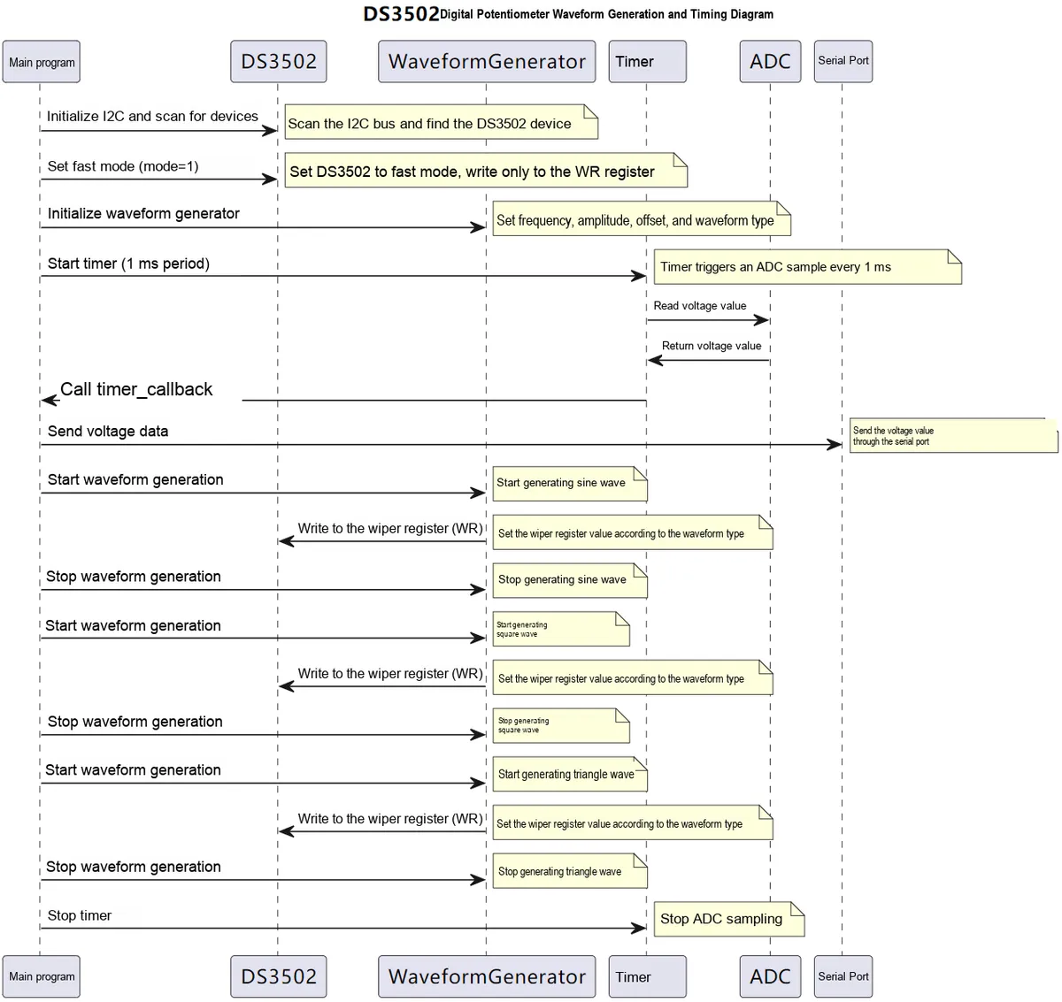
- First, perform the initialization operations: initialize the I2C bus, scan for and connect to the DS3502 digital potentiometer; initialize the serial port (UART) for data output, initialize the ADC for output voltage acquisition, and initialize the timer to trigger ADC acquisition at regular intervals.
- Waveform Generation: Use the
WaveformGeneratorclass to generate sine waves, square waves and triangular waves, and set the value of the sliding register (WR) via the DS3502 to control the output voltage. - Data Acquisition and Output: The timer triggers once every 1ms and calls
timer_callbackfunction to read ADC data, and sends the collected voltage value via the serial port. - Data output switching and stop: Each waveform stops generating after 5 seconds and switches to generate the next waveform, and finally the timer and ADC acquisition are stopped.
Next, we open the SerialPlot software, select the corresponding port connected to the USB-to-TTL chip, and click the Open button:

Data Format Selection ASCII encoding, with other configurations left as default:
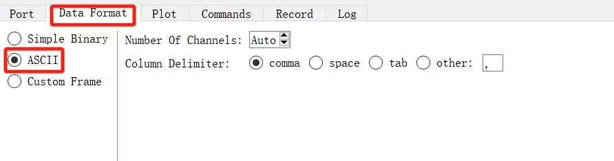
3.1 Application Experiment - PC Software Configuration.mp4 627 KB
Burn the code, open the terminal, and the output is as follows:
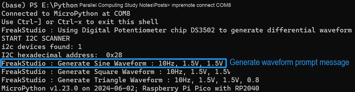
Open SerialPlot software, you can see that the frequency and amplitude of the displayed DAC output voltage are both normal:
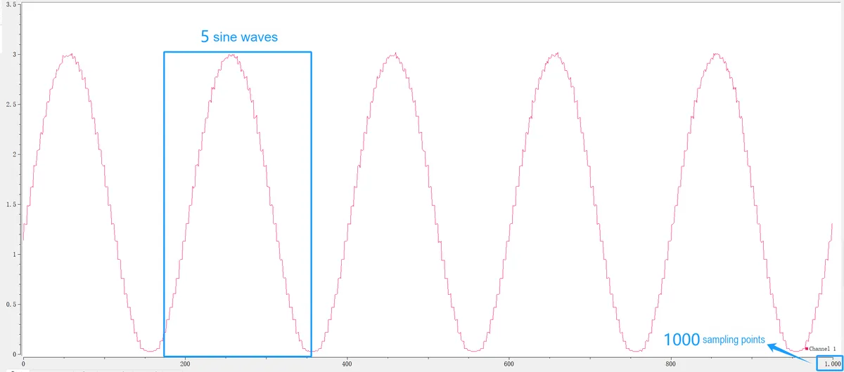
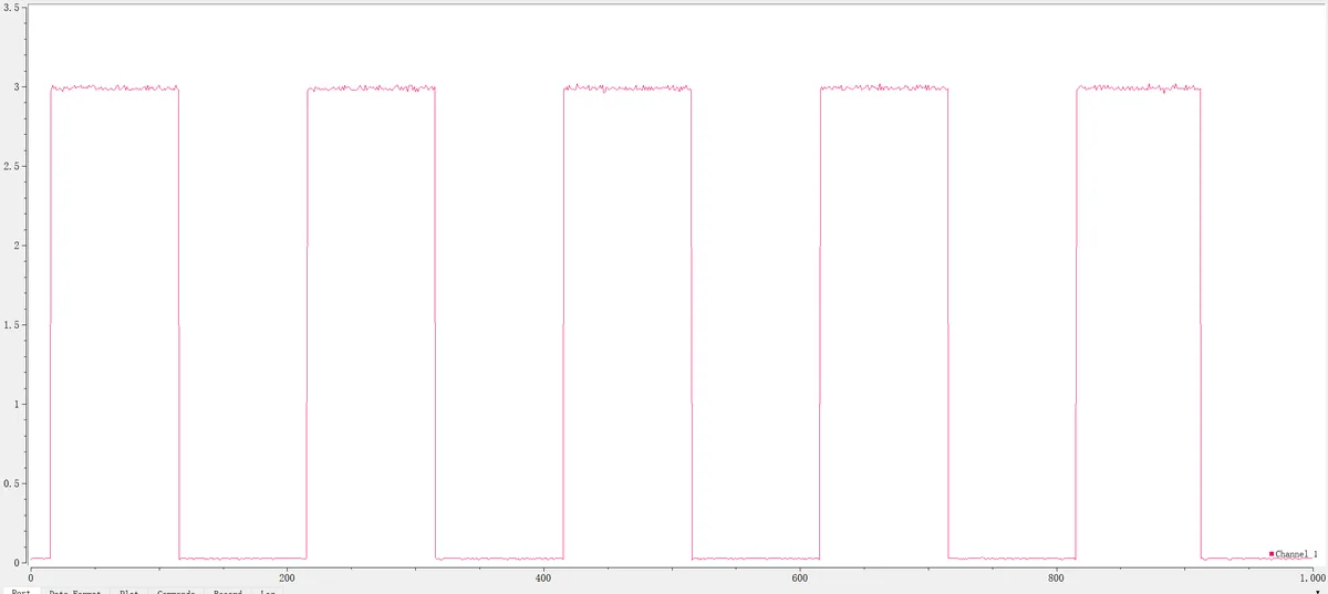
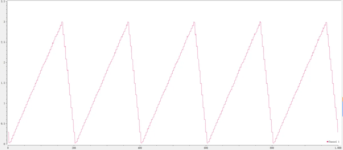
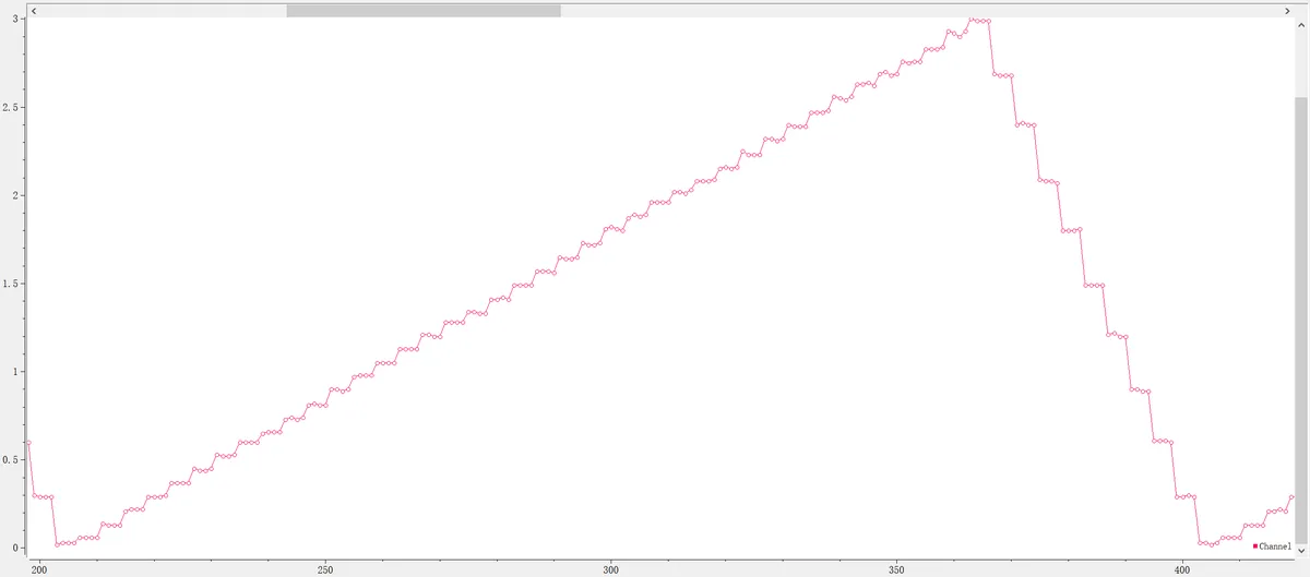
3.3 Application Experiment.mp4 9.5 MB
In the generated waveform, it can be seen that due to DS3502 having a low resolution (7 bits), the generated waveform has obvious steps, so it is not suitable for scenarios requiring high frequency or high precision.
3.4 Implementation of Waveform Generator Based on AD9833
In the following experiment, we need to insert the Fengya No. 1 Board - Adjustable DDS Signal Generation Board into the Fengya No. 1 Board - Universal Compatible Expansion Board, and at the same time turn on the Fengya No. 1 Board - Adjustable DDS Signal Generation Board 's SWITCH dip switch' s CS, SYNC, MOSI and MOSI options:
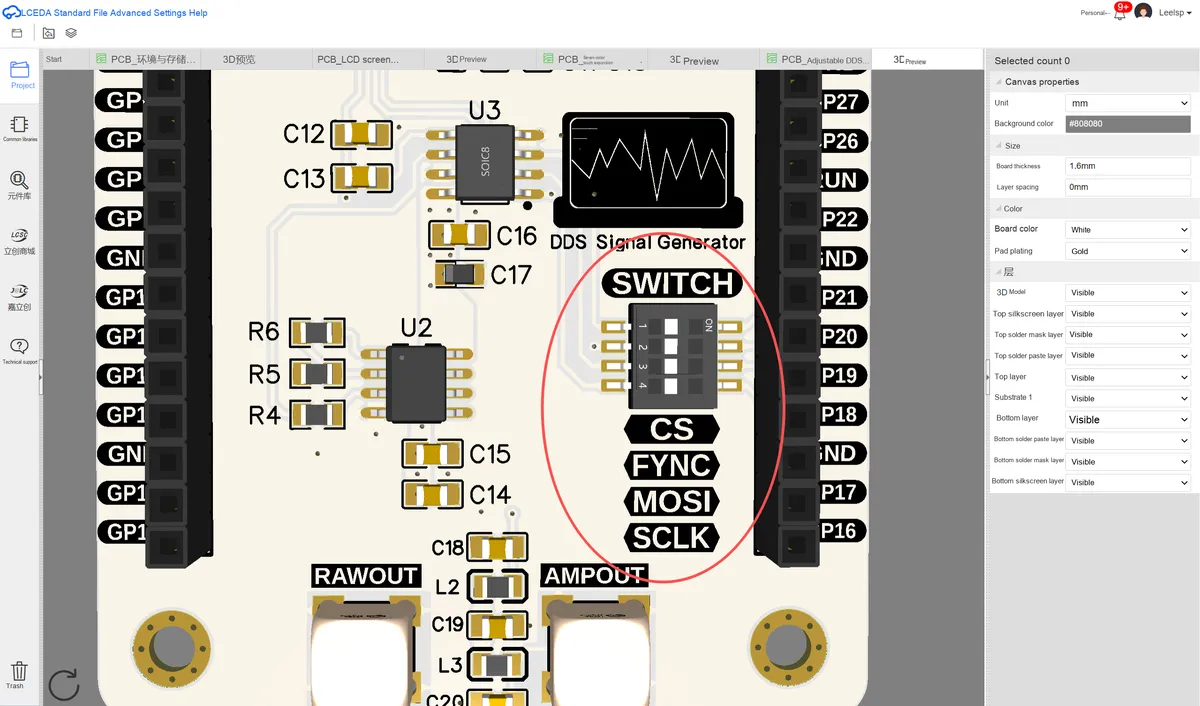
On our Fengya No. 1 Board - Adjustable DDS Signal Generation Board, the AD9833 chip section is equipped with a power supply π-type LC filter circuit; the output of the DDS signal generator is connected to the digital potentiometer section, which acts as a voltage divider, and its output is connected to a 6x non-inverting amplifier circuit, forming the AMPOUT amplified output. The schematic diagram is shown as follows:
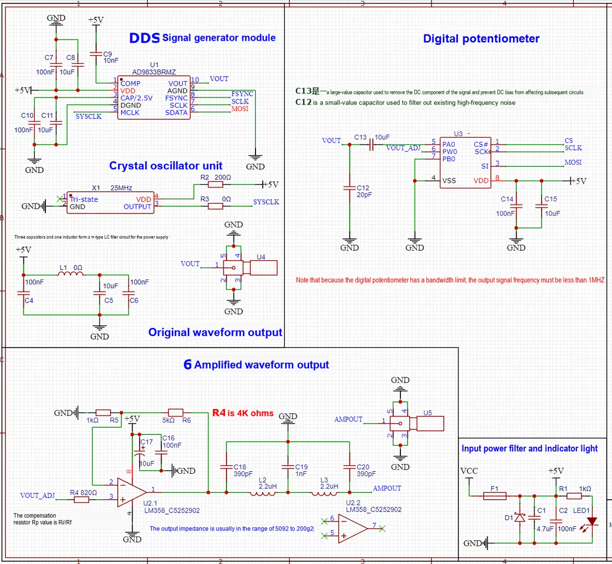
And at the signal amplification output terminal, DDS signal generation expansion module is equipped with a 5th-order low-pass filter with a cutoff frequency of 5.43 MHz. This filter functions to effectively reduce the high-frequency noise in the output signal and improve the signal quality, so that the generated waveform can better meet the requirements of high precision and low noise in experiments and testing scenarios that have high demands on signal quality.
Then we connect the SMA interface of the adjustable amplified output on the Fengya No. 1 Board - Adjustable DDS Signal Generation Board AMPOUT to the MCX interface of the DSO signal acquisition terminal on the oscilloscope via an SMA-to-MCX RF cable:
The wiring conditions of the components are shown in the following table:
Module/Chip | Description of the Name | Communication Method | Pico pins | chip pin | Supply Voltage | control level | Note |
AD9833 | DDS Signal Generator | SPI0 | GP18 (SCK) | CLK | 5V | 3.3V | The control terminal is compatible with 3.3V |
GP19 (MOSI) | SDATA | ||||||
GP20 (CS) | FSYNC | ||||||
GND | GND | common ground | |||||
VBUS | VCC | VBUS provides 5V power supply | |||||
MCP41010 | Digital Potentiometer | SPI0 | GP18 (SCK) | SCK | 5V | 3.3V* | Recommended level conversion for control terminal |
GP19 (MOSI) | SI | ||||||
GP21 (CS) | CS | ||||||
GND | GND | common ground |
At the same time, we will AD9833 and MCP41010 save the custom classes for them separately as ad9833.py file and mcp41010.py file:
The following code can be found in the elegance-devkit v1\Demo\64 DAC_Digipot folder of the resource package we provide.
In the following sample code, we use the AD9833 chip on the Raspberry Pi Pico to generate a DDS signal with adjustable frequency and phase, and adjust the signal amplitude via the MCP41010 chip. The sample code is as follows:
# Python env   : MicroPython v1.23.0
# -*- coding: utf-8 -*-
# @Time    : 2024/11/4 8:52 PM
# @Author  : Li Qingshui
# @File    : main.py
# @Description : Generate a DDS signal using the AD9833 chip and the MCP4725 chip, with adjustable amplitude, phase, and frequency

# ======================================== Import Modules =========================================

# Hardware-related modules
from machine import I2C, Pin
# Time-related modules
import time
# Import the AD9833 chip driver module
from ad9833 import AD9833
# Import the MCP41010 chip driver module
from mcp41010 import MCP41010

# ======================================== Global Variables ============================================

# ======================================== Functions ============================================

# ======================================== Custom Classes ============================================

# ======================================== Initialization ==========================================

# Power-on delay of 3 s
time.sleep(3)
# Print debug message
print("FreakStudio: Using AD9833 and DS3502 to implement DDS signal generator")

# # Create an AD9833 chip instance using the SPI0 peripheral: MOSI-GP19, SCLK-GP18, CS-GP20
ad9833 = AD9833(sdo=19, clk=18, cs=20, fmclk=25, spi_id=0)
# # Create an MCP41010 chip instance using the SPI0 peripheral: MOSI-GP19, SCLK-GP18, CS-GP21
mcp41010 = MCP41010(clk_pin=18, cs_pin=21, mosi_pin=19, spi_id=0, max_value=255)

# ========================================  Main Program  ===========================================

# Set the frequency and phase of the AD9833 chip
# Set the data of frequency register 0 and phase register 0
ad9833.set_frequency(5000,0)
ad9833.set_phase(0, 0, rads = False)
# Set the data of frequency register 1 and phase register 1
ad9833.set_frequency(1300, 1)
ad9833.set_phase(180, 1, rads = False)
# Select the frequency and phase of the AD9833 chip
ad9833.select_freq_phase(0, 0)

# Set the potentiometer value of the MCP41010 chip
mcp41010.set_value(125)

# Select frequency register 0 and phase register 0, and set the output mode of the DDS signal generator to sine wave
ad9833.select_freq_phase(0,0)
ad9833.set_mode('SIN')

# # Adjust the potentiometer value and observe the output waveform of the DDS signal generator
# mcp41010.set_value(20)
#
# # Select frequency register 0 and phase register 0, and set the output mode of the DDS signal generator to square wave
# ad9833.select_freq_phase(0,0)
# ad9833.set_mode('SQUARE')
#
# # Select frequency register 0 and phase register 0, and set the output mode of the DDS signal generator to square wave at half frequency
# ad9833.select_freq_phase(0,0)
# ad9833.set_mode('SQUARE/2')
#
# # Select frequency register 0 and phase register 0, and set the output mode of the DDS signal generator to triangle wave
# ad9833.select_freq_phase(0,0)
# ad9833.set_mode('TRIANGLE')
#
# # Select frequency register 1 and phase register 1, and set the output mode of the DDS signal generator to triangle wave
# ad9833.select_freq_phase(1,1)
# ad9833.set_mode('TRIANGLE')
Here, we first initialize the AD9833 chip and the MCP41010 chip, and then configure the two frequency registers and two phase registers of the AD9833 chip:
- Set register 0 to 5kHz with a phase of 0°.
- Set register 1 to 1.3 kHz with a phase of 180°.
Set the MCP41010 digital potentiometer to its midpoint value (125/255) to control the amplitude output of the analog signal, configure the AD9833 chip to use frequency register 0 and phase register 0, and set the output waveform to sine wave.
When flashing the code, the terminal output is as follows:
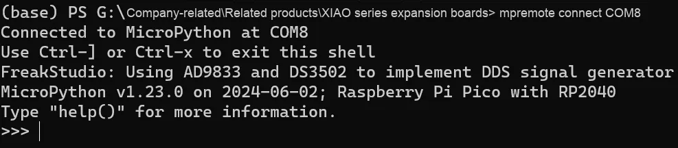
It can be seen that a sine wave is output. It should be noted that AD9833 is a unipolar DDS signal generation chip, and the waveform it generates is not a standard positive-negative symmetric waveform:
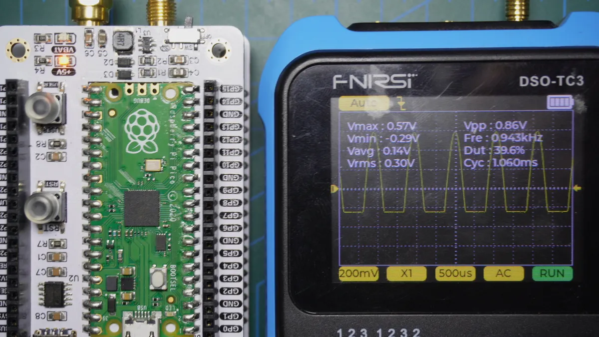
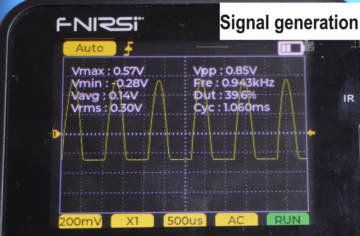
We use the mcp41010.set_value (20) command to adjust the potentiometer value of the MCP4725 chip, thereby regulating the signal amplitude:

It can be seen that the amplitude of the output waveform decreases:
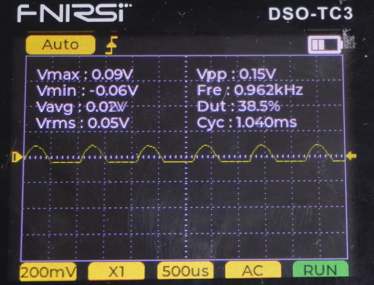
We can also enter the code in the comments into the command line one by one, and we will see that a square wave, a square wave with halved frequency, and a triangular wave are generated sequentially:
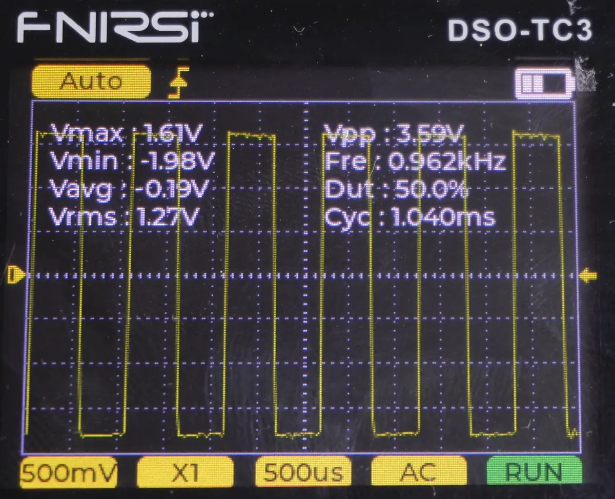
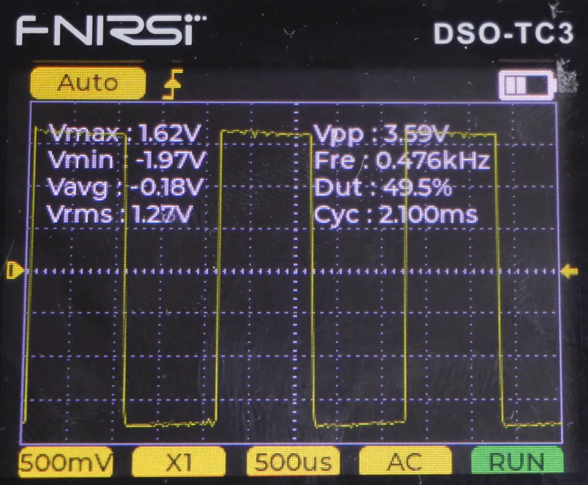
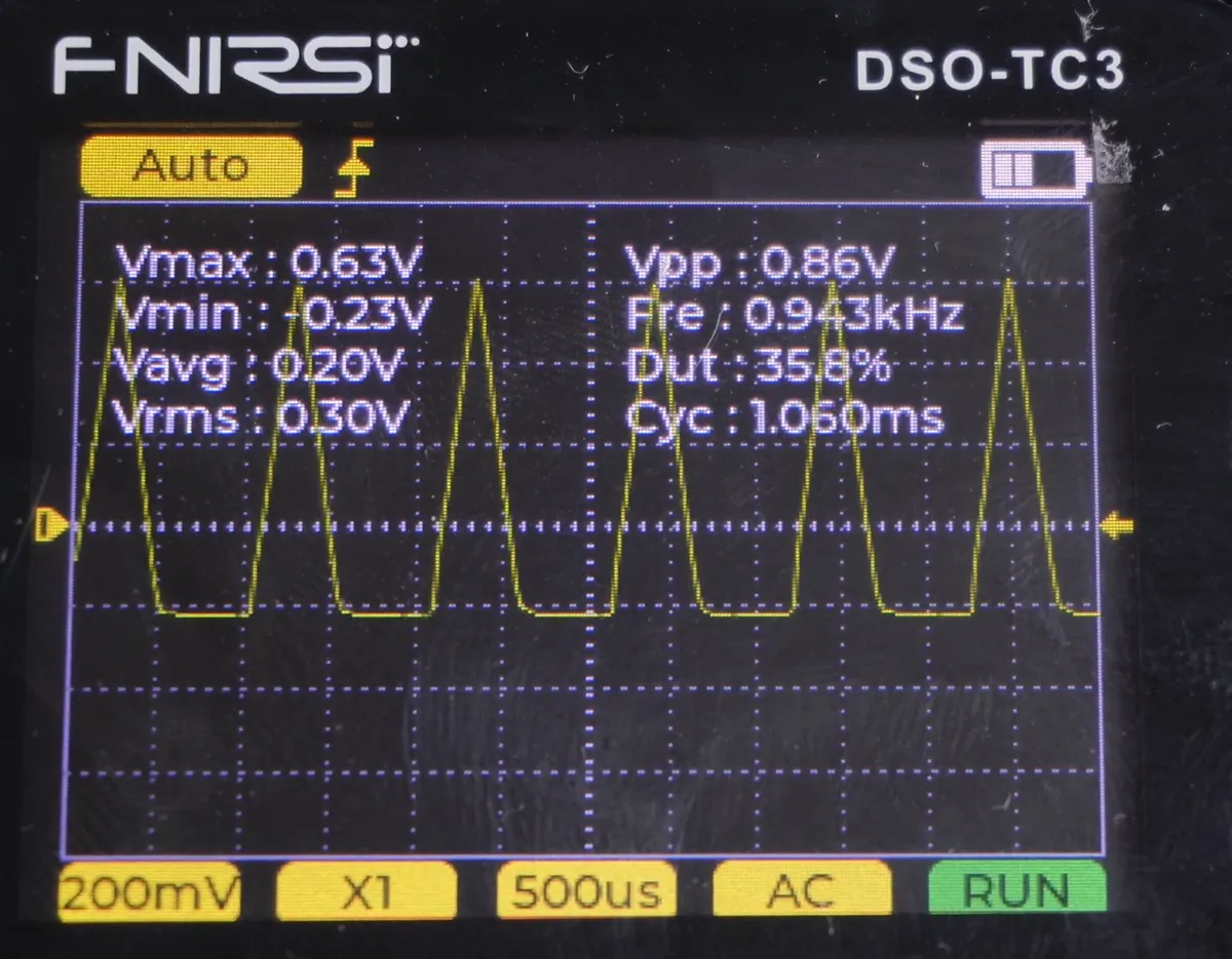
3.4 Application Experiment.mp4 84.0 MB
References
- Basic Principles of Digital-to-Analog Converters and Introduction to DAC Types
https://m.elecfans.com/article/431402.html
- Basic Principles of Digital-to-Analog Converters
https://www.mrchip.cn/newsDetail/618
- DAC Digital-to-Analog Converter
https://blog.csdn.net/wdxabc1/article/details/139691924
- Principle of DDS Signal Generator and Classic Design Schemes of DDS Signal Generators
https://blog.csdn.net/woshiyuzhoushizhe/article/details/101159860
- Digital-to-analog converter
https://en.wikipedia.org/wiki/Digital-to-analog_converter
- What is a DAC (Digital-to-Analog Converter) and How Does it Work
https://www.audioadvice.com/videos-reviews/what-is-a-dac-how-does-it-work
- Digital-to-Analog Converter
https://www.sciencedirect.com/topics/engineering/digital-to-analog-converter
- How Does a Digital to Analog Converter Work?
https://sciencing.com/analog-digital-converter-work-4968312.html
- The Basics of Direct Digital Synthesizers (DDSs) and How to Select and Use Them
https://www.digikey.com/en/articles/the-basics-of-direct-digital-synthesizers-ddss
- MCP4725 Driver Principle and Code Implementation – I2C Learning
https://blog.csdn.net/m0_46152793/article/details/124020512
- Notes on Peripheral Driver Library Development 48: MCP4725 Single-Channel DAC Driver
https://blog.csdn.net/foxclever/article/details/127716256
- MCP4725: 12-Bit Single Output DAC
https://www.microchip.com/en-us/product/mcp4725
- 2021 Electronic Competition Prediction: A Step-by-Step Guide to Mastering the DDS Module AD9833
https://blog.csdn.net/qq_39400113/article/details/119220659
- Notes on Peripheral Driver Library Development 4: AD9833 function Generator Driver
https://blog.csdn.net/foxclever/article/details/105172870
- AD9833-MicroPython-Module
https://github.com/owainm713/AD9833-MicroPython-Module/blob/main/AD9833.py
- micropython-mcp4725
https://github.com/wayoda/micropython-mcp4725
- A Simple Waveform Generator Implemented with DDS Chip AD9833
https://www.bilibili.com/read/cv27258951/
- 2. During the Electronic Design Competition. ..(Learning and Application of the AD9833 (DDS) Module)
https://blog.csdn.net/qq_67774643/article/details/131282649
- 2021 Electronic Competition Prediction: A Step-by-Step Guide to Mastering the DDS Module AD9833
https://blog.csdn.net/qq_39400113/article/details/119220659
- Adafruit DS3502 I2C Digital Potentiometer
https://learn.adafruit.com/ds3502-i2c-potentiometer/python-circuitpython
Version History
Version Number | Modifier | Time | Content |
v1.0.0 | Li Zisheng | 2025/09/19 | Initialize the document, based on MicroPython version v1.23.0. |
v1.1.0 | Li Zisheng | 2025/12/15 | Modified the image. |