
Contents
- I. Unboxing of Development Board and Modules and Hardware Overview
- 1.1 Appearance of RA4M2 Motherboard and DA14531 Module
- 1.2 Motherboard Version and Module Silkscreen
- 1.3 PMOD2 Interface and Connection Direction
- 1.4 Power Supply Jumper and Coin Cell
- 1.5 UART and SWD Interfaces
- 1.6 Type-C Buttons and LED Resources
- II. Analysis of DA14531 Resources and On-Board Circuits
- 2.1 Positioning of DA14531 Chip and BLE Application
- 2.2 Module Antenna and External Flash
- 2.3 Pmod Adapter Circuit and Reset Polarity
- 2.4 LPR and CONNECT Signals
- 2.5 Pin Correspondence of Motherboards and Modules
- III. Development Environment Setup and Project Preparation
- 3.1 Division of Responsibilities Between RA4M2 Main Control and Factory Firmware of Modules
- 3.2 e² studio and FSP Versions
- 3.3 Example of Motherboard LED and UART
- 3.4 SCI0 and Test Program Configuration
- 3.5 Follow-up Development Roadmap of DA14531 SDK6
- 3.6 Preparation of CH340 Driver and Download Tool
- IV. Program Download and Basic Experiment Verification
- 4.1 Motherboard Program Compile and Download
- 4.2 Serial Port Baud Rate Verification
- 4.3 AT Responses and Module Version
- 4.4 Mobile Phone Scanning and Connection
- 4.5 Bidirectional Data Transceiver
- 4.6 Troubleshooting Common Issues
- V. Short Text Transparent Transmission Program and Reproduction
- 5.1 Organization of the Dual Serial Port Test Program
- 5.2 Compile and Serial Port Download
- 5.3 Reproduction Steps on Mobile
- VI. Evaluation Summary
- 6.1 Completed Validation
- 6.2 Hardware Connection and Development Experience
- 6.3 Selection of AT Firmware and Secondary Development
- 6.4 Comprehensive Evaluation
- References
- Version Record
This experiment uses the RA ecosystem Studio RA4M2 V2.0 development board, paired with the DA14531 ultra-low-power Bluetooth Pmod module, to verify BLE data communication between the mainboard and a mobile phone. The RA4M2 is responsible for application logic and UART transmission and reception, while the DA14531 module completes advertising, connection and data transmission via its factory-default AT firmware.
We have successfully tested the LED routine, serial port printing, module AT query, and two-way transparent transmission of short text between the mobile phone and the device. When the mobile phone sends 123, the RA4M2 receives the bytes 31 32 33 and performs a postback, and the mobile phone also completes the round-trip display of "Hello Renesas". For developers who want to add BLE communication to existing MCUs, this combination can first complete prototype verification with the factory AT firmware via UART.
I. Unboxing of Development Board and Modules and Hardware Overview
1.1 Appearance of RA4M2 Motherboard and DA14531 Module
The RA4M2 motherboard adopts a 100-pin MCU, and is equipped with a Type-C interface, a CH340 USB-to-serial circuit, an SWD debug interface, a Pmod expansion interface, user buttons, LEDs and capacitive touch buttons. When used for Bluetooth evaluation, these resources can undertake the tasks of power supply, log observation, program download and local interaction respectively.
The DA14531 module is connected to the mainboard via a Pmod connector. The blue baseboard provides the connector and supporting circuitry, while the small green board integrates the Bluetooth chip, antenna and related components. This setup allows for serial communication between the mainboard and the module to be implemented first, before extending to mobile phone control and sensor data upload.
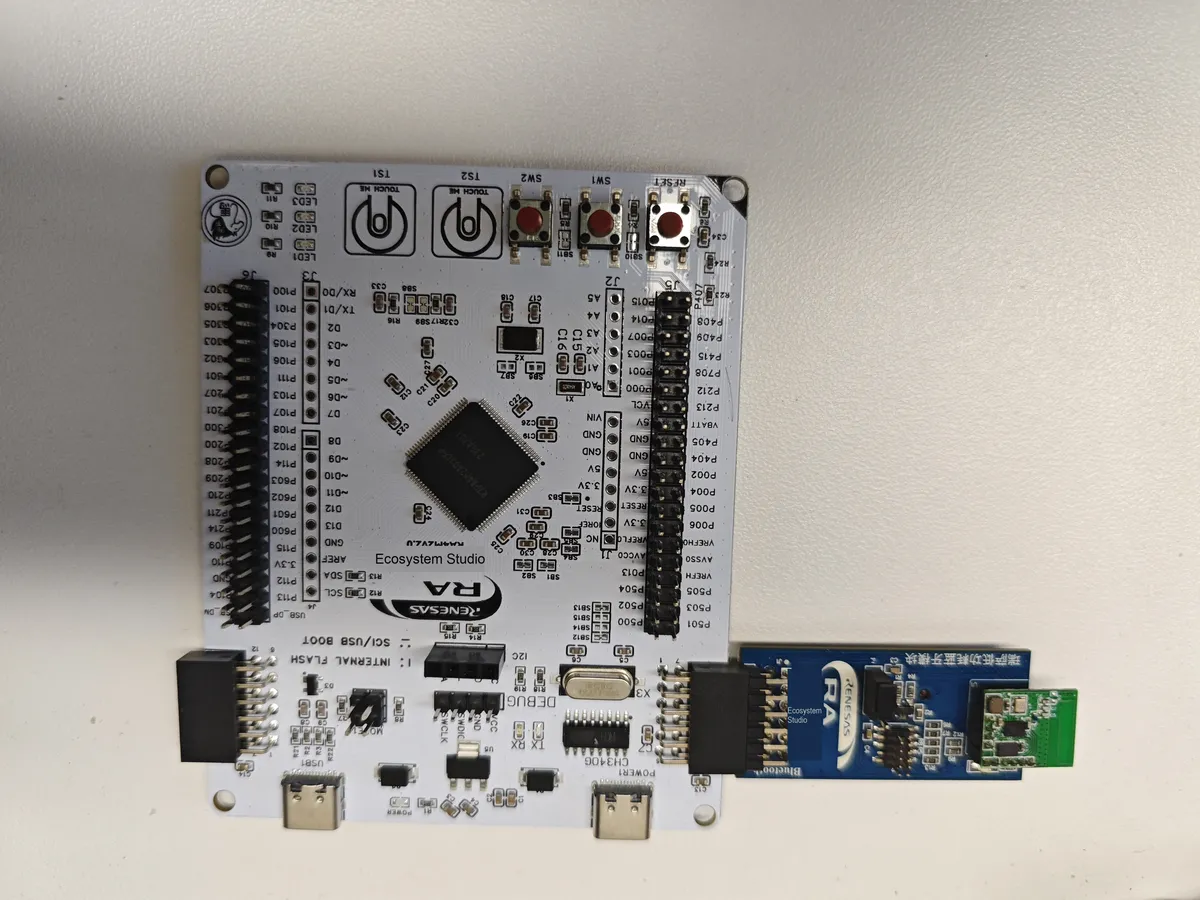
Figure 1: The physical connection between the motherboard and the module this time, with the original orientation retained in the photo.
1.2 Motherboard Version and Module Silkscreen
The silkscreen on the motherboard photo reads "RA4M2 V2.0". The development board manual and schematic diagrams in the supporting documentation package are labeled V1.0, and the target device in the project configuration is R7FA4M2AD3CFP. Therefore, this paper takes the physical V2.0 as the evaluation object, the old version of the materials is used to understand the circuit and project structure, and the specific pin and crystal oscillator configurations shall be verified during wiring and debugging.
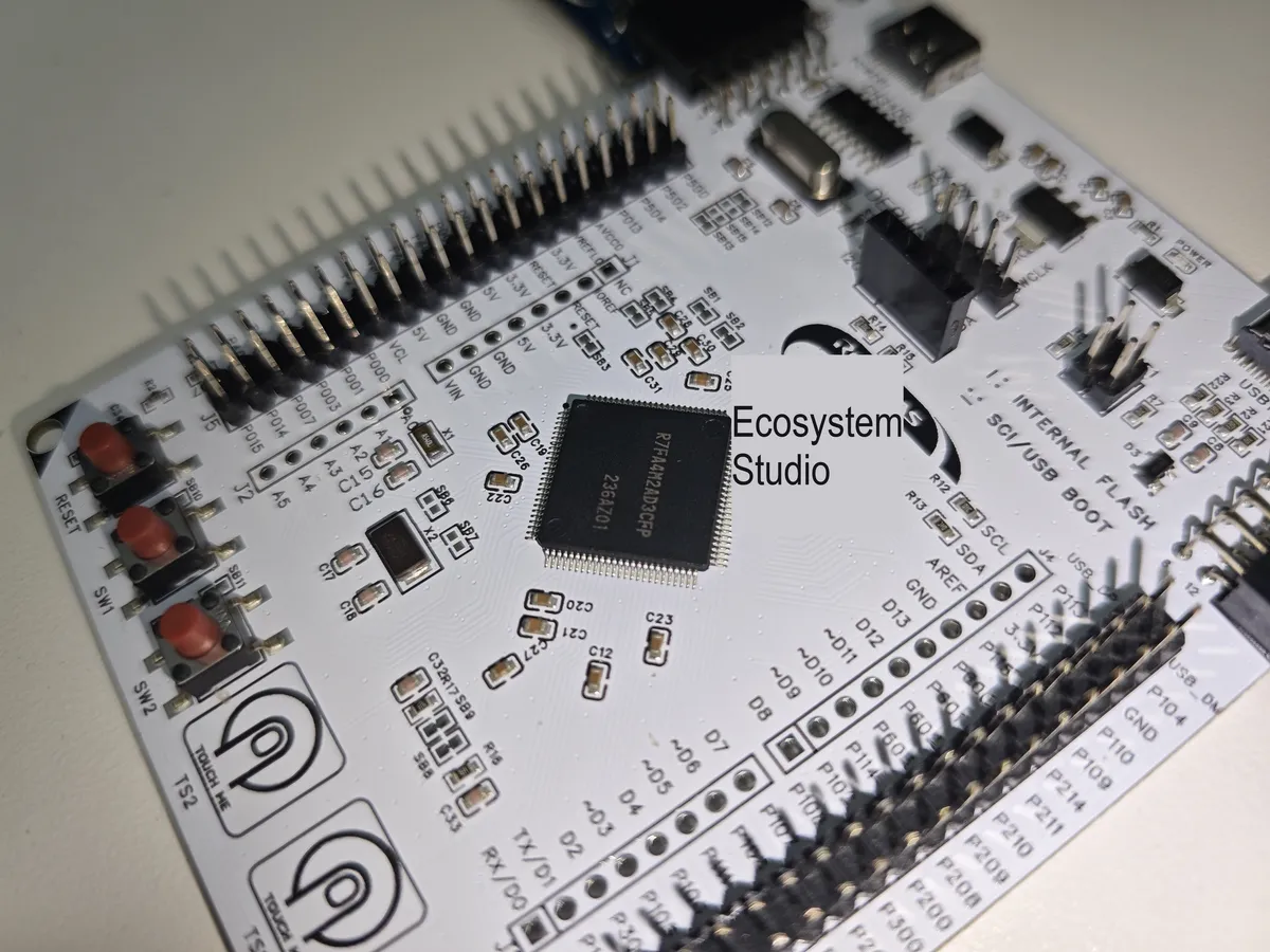
Figure 2: The markings of the visible MCU model R7FA4M2AD3CFP and the RA4M2 V2.0 identifier are shown, with the surrounding expansion header pins, buttons and touch area also presented.
The module materials include the Bluetooth usage instructions, the schematic of the Pmod baseboard, the schematic of the SF-BLE-DA14531 small module, and the DA14531 datasheet. For first-time use, please read the module usage guide first, which allows you to quickly get familiar with the UART parameters, control signals and mobile phone testing process.
1.3 PMOD2 Interface and Connection Direction
The Pmod interface integrates power supply, ground, UART and control signals into a single connector, making it suitable for adding wireless communication capabilities to the motherboard. When in use, confirm Pin 1, connection orientation and power supply first, then check the UART transmission and reception direction, and avoid judging the wiring only based on the shape of the connector.
According to the schematic diagram in the data package, P411/TXD0 of the motherboard PMOD2 corresponds to the RXD of the module, and P410/RXD0 corresponds to the TXD of the module; CONNECT and LPR are used to read the connection status and control the working status of the UART respectively. For the complete comparison table, refer to the Wiring and Test Plan (see the data package at the end of the article). The SCI0 communication and control signals this time have passed the V2.0 physical joint debugging.
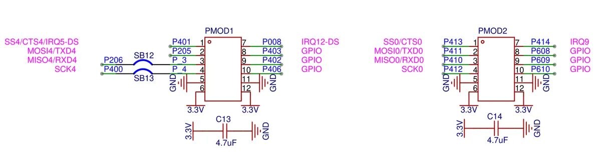
Figure 3: The complete PMOD1 / PMOD2 interface area in the V1.0 schematic, including all 12 pins, signal names on both sides, GND, 3.3V and decoupling capacitors; the Bluetooth module this time uses the PMOD2 on the right.
1.4 Power Supply Jumper and Coin Cell
The module baseboard is equipped with a power selection circuit and a coin cell holder, facilitating switching between motherboard power supply and standalone operation. For the initial joint debugging, use the 3.3V power supply provided by the motherboard, verify the power jumper according to the baseboard schematic, and remove the coin cell at the same time to reduce the impact of the power supply path on debugging and current measurement.
The module operation specification stipulates that the power supply for the module is 3.0–3.3V. The 5V power supply mentioned in the manual is applicable to the input of specific USB adapter boards and cannot be directly connected to the 3.3V terminal of the module. In subsequent low-power measurement, it is necessary to clarify whether the instrument measures the Bluetooth module branch or the complete motherboard, and record the impact of circuits such as the indicator lights on the baseboard.
1.5 UART and SWD Interfaces
UART is the application communication channel between the current motherboard and the Bluetooth module. The RA4M2 sends AT query or setting commands to the module, which returns responses; after the mobile phone is connected, the UART also undertakes bidirectional transmission of test data. The module manual requires that AT commands end with a carriage return and line feed, so the program should include \r\n when sending.
The onboard CH340 is used for USB-to-serial conversion. It is necessary to distinguish between the computer's COM port where the CH340 is located and the MCU serial port used by the Bluetooth module: according to the circuit in the documentation package, CH340 corresponds to SCI9, while PMOD2 uses SCI0. After the computer opens the onboard serial port, it cannot directly assume that the received data comes from the DA14531, and the motherboard program needs to implement corresponding forwarding or log output functions.
SWD is used for firmware download and online debugging, and is suitable for variable observation, breakpoint setting and troubleshooting. The SWD interfaces of the RA4M2 mainboard and the DA14531 baseboard are for different chips respectively, so the target interface needs to be confirmed before downloading. The current module test retains the factory firmware of DA14531, so the program on the RA4M2 side shall be written first.
1.6 Type-C Buttons and LED Resources
The motherboard provides a Type-C interface marked USART and a native USB interface, and the circuits connected to the two are different. When using the USB-to-serial function, you should select the USART interface and use a cable that supports data transmission. If no COM port appears on the computer, you can check the interface, cable, power supply and CH340 driver in sequence.
The reset button, two user buttons, two touch areas, and three LEDs on the board serve as basic experimental resources. You can first use the LEDs to verify whether the program is running, then trigger Bluetooth transmission via the buttons or control the LEDs through a mobile phone to make the test phenomena more intuitive. The LED experiment also acts as the starting point for checking the clock, GPIO configuration, and programming process.
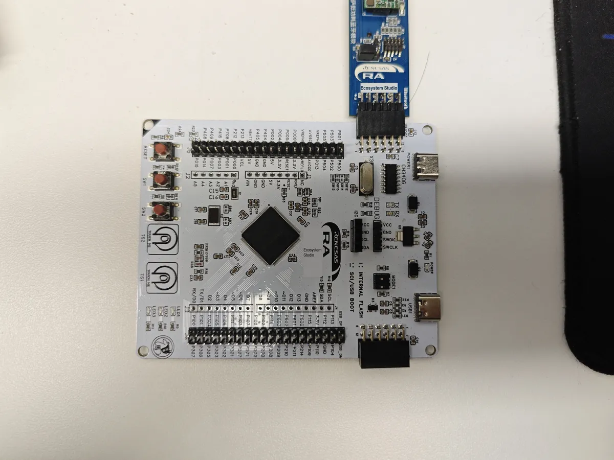
Figure 4: Shows the relative positions of the two Type-C ports, DEBUG interface, MODE jumper, buttons, touch area and LEDs; the module is located at the top of the photo, with the antenna end outside the frame, and the complete module is shown in Figure 5.
II. Analysis of DA14531 Resources and On-Board Circuits
2.1 Positioning of DA14531 Chip and BLE Application
The DA14531 is a System-on-Chip (SoC) designed for Bluetooth Low Energy (BLE) applications, featuring a 16MHz Arm Cortex-M0+ core, 48KB RAM, 144KB ROM, 32KB OTP, and integrated peripherals including UART, SPI, I²C and ADC. This chip supports Bluetooth 5.1 BLE; its specific functions shall still be verified against the datasheet, as the version number does not directly represent all optional features. The AT firmware preloaded on the module was used for this test, with the RA4M2 handling the main application logic.
This division of labor delegates BLE advertising, connection, and GATT processing to the module, while the main controller exchanges data via the serial port, making it suitable for sensing data reporting, simple configuration, and device status interaction. The transparent transmission described in this paper is built on the BLE GATT service, and the mobile phone needs to select the corresponding characteristic and enable notifications.
2.2 Module Antenna and External Flash
The schematic of the SF-BLE-DA14531 small board includes the DA14531, a 32MHz crystal, RF matching components, a PCB antenna, and an external SPI Flash. The 32MHz refers to the frequency of the crystal shown in the diagram, which describes a different component from the 16MHz operating frequency of the chip's CPU. The capacity of the Flash device in the provided documentation is not specified, and this document does not presume it to be any fixed capacity.
The blue Pmod baseboard is responsible for connection and power supply matching, while the small green board carries the main wireless circuit. During use, space should be reserved for the antenna area to avoid being shielded by close proximity to metal enclosures or large-area grounded copper foils. This round of testing only verifies short-range functionality, and no extrapolation of communication range or antenna performance is made based on this.
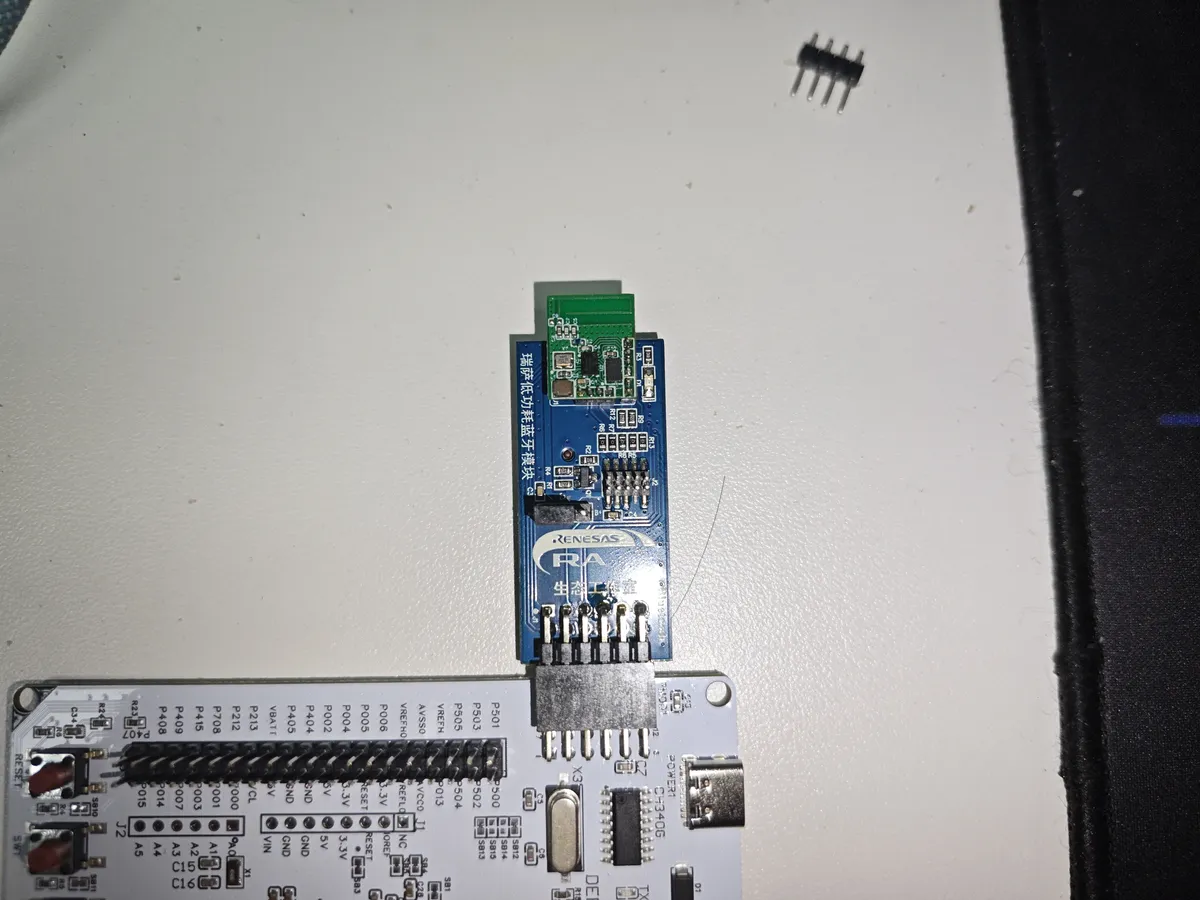
Figure 5: Shows the PCB antenna, device area of the green wireless small board, as well as the connection direction between the blue adapter base plate and the motherboard. This photo is for appearance and interface observation, and the device functions shall be subject to the supporting schematic diagram.
2.3 Pmod Adapter Circuit and Reset Polarity
The RESET pin of the module body is active-high, whereas the Pmod baseboard integrates an SS8550 transistor inverting circuit into the reset control path. Therefore, in this program, the P412 pin of the RA4M2 remains at a high level to release the reset, and pulling it low will trigger the module reset via the baseboard. When directly connecting the small module or using the Pmod baseboard, the polarity must be determined according to the respective circuit.
The target of this programming is always RA4M2, and the factory-default AT firmware of DA14531 shall be retained; the Boot mode selection of the motherboard and the firmware download of the module itself are two independent processes.
2.4 LPR and CONNECT Signals
LPR is used to control the UART working status of the module; this time, P609 is output as high level to enable the serial port. CONNECT is an output of the module and an input of the motherboard, and reading a high level via P414 indicates a successful connection. After actual testing of mobile phone connection, the connect in the motherboard log changes from the disconnected state to 1.
BOOT corresponds to P413, which is configured as an input this time without active driving. For low-power applications, further arrangements are required for UART sleep, wake-up and the working cycle of the main controller; the current debug configuration that keeps LPR at high level is not a result of power consumption optimization.
2.5 Pin Correspondence of Motherboards and Modules
The following mappings are derived from the supporting V1.0 schematic diagram, and the relevant UART, LPR, RESET and CONNECT have been used in this V2.0 physical short text test.
PMOD2 Pin | RA4M2 Signal | Module Purpose / Current Configuration |
|---|---|---|
1 | P413 | BOOT, set the motherboard to input |
2 | P411 / TXD0 | Connect to module RXD |
3 | P410 / RXD0 | Connect to module TXD |
4 | P412 | Base plate reset control, released at high level |
5, 11 | GND | commons |
6, 12 | power supply | Use 3.3V, verify and select per J3 |
7 | P414 | CONNECT, motherboard input |
8 | P608 | Module-side NC |
9 | P609 | LPR, the motherboard outputs a high level |
10 | P610 | Module-side NC |
III. Development Environment Setup and Project Preparation
3.1 Division of Responsibilities Between RA4M2 Main Control and Factory Firmware of Modules
This Development Environment consists of e² studio, RA FSP, compile toolchain and download tools. e² studio is responsible for engineering management, compile and debugging; FSP provides configuration for BSP, clock, pins and peripheral drivers; the compiler compiles the source code into an executable file; the download tool is in charge of flashing the program into the target chip. The serial port tool is used for observing logs and verifying module command responses.
In the first phase, the RA4M2 runs the test program, which uses the factory AT firmware of the DA14531 via UART to complete version query, mobile phone connection, and data transmission and reception. This phase mainly utilizes the GPIO and UART drivers of the RA FSP. If there is a need to modify the GATT service of the DA14531 or enable the Bluetooth chip to run applications independently later, development will then proceed with the SmartBond SDK6.
3.2 e² studio and FSP Versions
When setting up the environment for the RA series, you can directly select the FSP integrated installer that includes e² studio to reduce the version matching work between the IDE, configurator and toolchain. e² studio 2026-07 and FSP 6.6.0 have been installed on this computer, and it is confirmed that the installation directory contains the RA4M2 device support package.
The installation process is as follows:
- Open the official release page of Renesas FSP, select the Windows installer
setup_fsp_v6_6_0_e2s_v2026-07.exe. - Run the installer, select Quick Install or Custom Install as needed, and check the IDE, FSP and compile toolchain components.
- Use an English installation path, then launch e² studio and select a standalone workspace.
- Confirm the recognized toolchain in the IDE, then select the compiler required by the project.
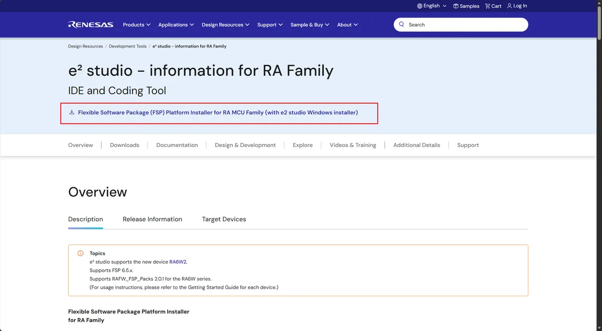
Figure 6: The RA FSP integrated installation entry in the reference article, showing the download location; the specific version used this time is FSP 6.6.0.
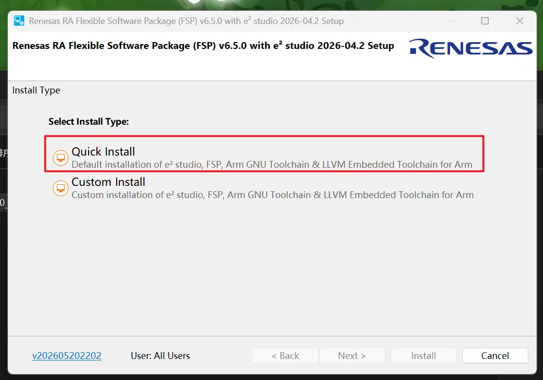
Figure 7: Schematic diagram of the installation interface of the reused reference article, the screenshot versions are FSP 6.5.0 and e² studio 2026-04.2, which are used for identifying installation options.
This machine is also installed with Arm GNU Toolchain 13.3 and GNU Arm Embedded Toolchain 10.3, which have been verified to be operational via version commands. The projects in the original materials mainly use FSP 3.2.0, while some examples use 3.6.0 or 4.0.0; the mere fact that the IDE is installed does not guarantee that old projects can be directly compile.This working copy was actually built by compile using GCC 10.3, the GNU Make bundled with e² studio, and the FSP 3.2 source code included in the supporting materials this time; it has not been migrated to FSP 6.6.0. Installing a new version of the IDE and actually building with a new version of FSP are two separate matters.
3.3 Example of Motherboard LED and UART
The resource package provides 14 examples covering peripherals and components including LED, UART, ADC, DAC, PWM, GPIO, RTC, touch sensor and OLED. For the complete list and version information, refer to the motherboard example index (included in the resource package at the end of the document). It is recommended to start with RA4M2LED to verify program download and GPIO output, then refer to RA4M2PRINTF and RA4M2USRT to get familiar with the UART driver.
Use English names for project paths. board/examples/ retains vendor examples, modules/DA14531/firmware/ is used for the project of this work, modules/DA14531/results/ stores logs and screenshots. The Workspace of e² studio can be separately set to C:/Renesas/workspace/RA4M2_BLE/, and use a copy when importing the project to retain the original files for comparison.
When importing an existing project, use the Existing Projects into Workspace option under File → Import, and select the directory where the RA4M2LED working copy is located. Importing an existing project retains the startup files, linker scripts, FSP configuration, and build options, making it easier to reproduce than only copying C source code. In addition to the src/ source code, each project also includes configuration.xml, FSP configuration and generated files; the peripheral instances, pin multiplexing, and clock settings all need to be checked together.
RA4M2USRT Keep the original name of the resource package. The default UART configuration uses SCI9 with a baud rate of 115200. When used for PMOD2 Bluetooth communication, it needs to be changed to the corresponding SCI0 and the actual baud rate of the module.
3.4 SCI0 and Test Program Configuration
Open configuration.xml, then check the following items one by one:
Page or settings | Inspection Content |
|---|---|
BSP or Summary | The target is RA4M2, and the engineering device model |
Clocks | The frequency of the external crystal oscillator matches the physical product; the old documentation indicates it may be 12MHz or 24MHz. |
Pins | Use the RA4M2 pin configuration to verify the actual connections of the LED, UART and Pmod |
Stacks | Complete settings for UART instances, channels, baud rates, callbacks and interrupts |
Project Properties | The selected FSP and compiler versions are available, and the linker script and build configuration are correct. |
The crystal oscillator parameter of the original project is 24MHz. This time, the existing configuration was reused to complete the functional verification of LED, PRINTF and BLE; no separate clock accuracy measurement was performed. The above table is applicable for project inspection or migration. In this dual-serial-port test project, SCI0 is directly configured, and interrupt vectors are manually added. configuration.xml has not fully synchronized these changes; when reproducing the project, use the attached command-line build process, and directly clicking Generate Project Content may overwrite the manual configuration.
For the Bluetooth test project, first configure the r_sci_uart driver and the corresponding GPIO. According to the schematic in the data package, the TXD0/P411 of SCI0 is connected to the RXD of the module, and the RXD0/P410 of SCI0 is connected to the TXD of the module; the LPR must be kept at a high level to use the UART, and the CONNECT serves as a motherboard input to monitor the connection status. The reset signal passes through the inverting circuit on the base board, so the polarity of the module body and the Pmod control terminal must be distinguished.
The serial port format adopts 8 data bits, no parity, and 1 stop bit. The module specification contains two descriptions of the default baud rate, 38400 and 115200, so send AT? \r\n at 38400 first; if there is no valid response, check the wiring and try 115200, and finally record the actual value of the current module.
The program opens the serial port via R_SCI_UART_Open, and sends commands via R_SCI_UART_Write. It collects received bytes in the callback UART_EVENT_RX_CHAR, records transmission completion in UART_EVENT_TX_COMPLETE, and then parses responses and processes data in the main loop. A successful return from the serial port write function only indicates that the transmission request has been accepted; when transmitting continuously, it is still necessary to wait for the completion event, and set timeouts and buffer boundaries.
If migration and reconfiguration are performed within the IDE, you shall execute Build Project again and check the results; this actual test adopts command-line build. The ELF file contains programs and symbols for debugging, HEX or SREC is used for the supporting programming process, and the MAP file helps analyze the memory distribution of the program. Some projects in the resource package include Debug/ historical artifacts, which shall be recompile in this test, and the output file name, generation time and target configuration shall be confirmed according to the build log.
Currently, the installation checks for the IDE, FSP support package, and native GCC have been completed, and the full compile of the three basic routines including LED, PRINTF, and USRT has been finished using GCC 10.3 and the GNU Make bundled with e² studio. The build adopts the FSP source code provided in the data package, corrects the old absolute paths in the working copy, and does not perform re-generation after FSP 6.6.0 configuration. There are 8 warnings in PRINTF and 4 warnings in USRT, and none of the three routines has compile errors;The LED routine has completed serial port programming and verification, and the user confirms that the LEDs on the board flash alternately; the dedicated Bluetooth test project has also completed compile, programming, and physical AT and short text echo verification, with the source code located at modules/DA14531/firmware/RA4M2_DA14531_AT/.
3.5 Follow-up Development Roadmap of DA14531 SDK6
After completing AT communication on the mainboard side, use DA14531's SmartBond SDK6 only if you need to customize GATT services, advertising logic, and low-power behavior. SDK6 and RA FSP are designed for Bluetooth chips and RA MCUs respectively, and differ in both project structure and tool configuration.
You can follow the official getting-started tutorial for SDK6 to get started with the bare peripheral template, and adapt GPIO, UART and external Flash according to the actual modules. Before flashing the firmware, prepare a restorable original AT firmware or a valid backup first, and give priority to using RAM download for program verification. For detailed steps, refer to the Development Environment description (see the resource package at the end of the article).
3.6 Preparation of CH340 Driver and Download Tool
After the motherboard is connected to a computer via the USART Type-C interface, the corresponding COM port should appear in the Device Manager. If it is not recognized, check the CH340 driver and the data cable. When using a serial port assistant or download tool, only one program should occupy the same port to avoid connection failures.
This time, we use the command-line tool bundled with Renesas Flash Programmer V3.25 to download the RA4M2 program via serial bootloader over CH340's COM6 port at 9600 bps, and complete the erase, write and verification processes. Before downloading, switch the MODE to SCI/USB BOOT and reset the device; after downloading, switch it back to INTERNAL FLASH and reset again. The COM port number varies with the computer and USB port, and shall be subject to the Device Manager.
The programming of the RA4M2 and the firmware update of the DA14531 module are handled separately. The factory-default AT firmware of the Bluetooth module is retained for now; Bluetooth tools such as the SmartBond Flash Programmer will be used in subsequent module firmware development.
IV. Program Download and Basic Experiment Verification
4.1 Motherboard Program Compile and Download
The compile results of the basic routines are as follows, and all outputs come from the rebuild after clearing the old object files in the copy:
Engineering | compile result | burning file |
|---|---|---|
RA4M2LED | 0 errors, 0 warnings |
|
RA4M2PRINTF | 0 errors, 8 warnings |
|
RA4M2USRT | 0 errors, 4 warnings |
|
For detailed construction methods and boundaries, refer to the compile record (see the resource package at the end of the article). These results confirm the command-line compile chain, and after downloading, you still need to check the actual behavior of the clock, LEDs, and serial port of the V2.0 board.
On November 6,2026, the command-line tool of RFP V3.25 was used to successfully connect via COM6,9600 bps, two-wire UART to the R7FA4M2AD3CFP, and read Boot Firmware V1.6.25. The erasing, writing and verification of the LED program were all completed, the tool returned code 0, and displayed Operation successful.The erased Code Block this time is 0x00000000–0x00001FFF, and the write and verification range is 0x00000000–0x00000B7F. After programming, switch MODE back to INTERNAL FLASH and reset the device. After the user confirms that the LEDs on the board flash alternately, the entire process from compile, download to actual operation of the basic routine is fully functional.
After the first round of chip identification, the second connection once encountered E3000105 "Device not responding"; after keeping SCI/USB BOOT pressed and pressing RESET, the re-burning was successful. For the complete record, please refer to the burning log (see the data package at the end of the article).
4.1.1 LED Program Running Screen
After switching MODE back to INTERNAL FLASH and performing a reset, the on-board LEDs toggle their on/off status as programmed. The panoramic view below shows the mainboard power supply, the RA4M2 V2.0 silkscreen, and the illuminated LED3; the status comparison diagram further presents the output combinations at different times, making it convenient to observe the program operation phenomenon for comparison.
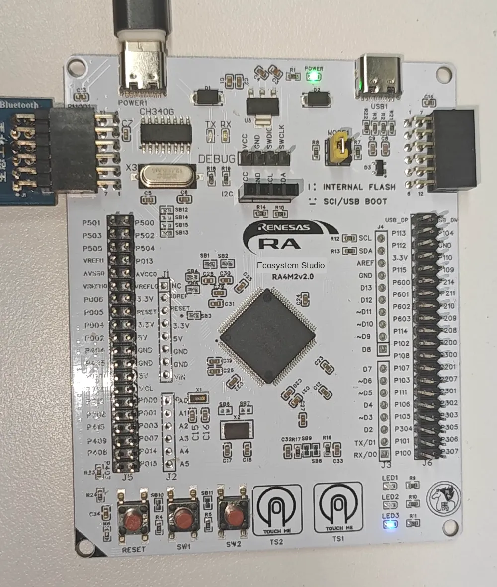
Figure 8: Overview of the LED routine in operation, captured from the actual measurement video at approximately 0.18 seconds. The frame has been rotated to orient the text correctly and cropped to remove irrelevant background.
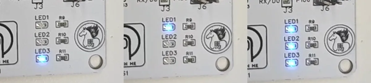
Figure 9: The frames are taken from the video at approximately 0.18s, 1.18s and 2.68s from left to right, corresponding to the states where LED3 is lit alone, LED1 is lit alone, and all three LEDs are lit simultaneously. The partial frames have been cropped, rotated, scaled up proportionally, and then spliced in chronological order.
Check the original LED measurement video (see the resource package at the end of the article). The original video file remains unchanged; three independent screenshots are located at assets/images/board-led/, and the frame extraction positions and processing parameters are specified in the creatives record (see the resource package at the end of the article).
4.2 Serial Port Baud Rate Verification
After the LED verification is completed, program via COM6 RA4M2PRINTF.srec. RFP returns success, and the erasure, writing and verification of the code area are all completed. After programming, switch MODE back to INTERNAL FLASH, then press RESET, and the computer receives the serial port output at 115200 baud rate, 8N1, no hardware flow control.
The actually captured output snippet is as follows:
RA E2STUDIO
Hello World!.
int_i=55
float_i=66.20
char_i='hello e2studio'
int_i=55
float_i=66.20
char_i='hello e2studio'
The integers, floating-point numbers and strings all conform to the program settings, and the subsequent content is output continuously and repeatedly. This result verifies the serial port printing link from the motherboard SCI9 to the computer COM6 via CH340, and the records are available in the original serial port log (see the data package at the end of the article) and the PRINTF programming log (see the data package at the end of the article).
The value 115200 here refers to the parameters of the motherboard log serial port. The DA14531 uses SCI0 on PMOD2, and the baud rate of its AT firmware needs to be verified independently, which has also been confirmed to be 115200 this time.
4.3 AT Responses and Module Version
The dedicated main control test program retains the factory firmware of the DA14531, uses SCI9 for the computer log port, and SCI0 for module communication. After the program detects baud rates of 38400 and 115200, it receives a valid AT response at 115200, then completes parameter query, with both serial port error count and packet loss count being 0.
Query Item | Current module returns |
|---|---|
Software Version |
|
Broadcast Name |
|
Module UART Baud Rate |
|
Transmit Power Level |
|
Broadcast Interval Configuration |
|
Connection Interval Configuration |
|
The above is the current module configuration, which is different from the Default Value in the manual; the connection interval also needs to be distinguished from the actual BLE negotiation result. The original bytes and parsing records can be found in the startup log (see the resource package at the end of the article) and the AT query result (see the resource package at the end of the article). During the test, send AT+ ADV= 1, the module returns OK+ ADV, and no parameter saving or factory reset command is executed.
4.4 Mobile Phone Scanning and Connection
The mobile phone BLE debugging app has scanned the module. During the connection process, the motherboard reads a high CONNECT level, and the log shows connect= 1. On the mobile phone side, please select the corresponding write and notification characteristics in the custom service.
Bluetooth serial port application is adopted for the mobile terminal this time. Click the gear button on the right side of the module to open "Select BLE transparent transmission parameters", and fill in the following services and features; the content has been checked and confirmed to be consistent with the supporting manual and the actual measured mobile phone screen.
Configuration Item | UUID |
|---|---|
Custom Service |
|
Mobile phone sends Write feature |
|
The mobile phone receives the Notify characteristic |
|
First enable notifications for the Notify characteristic, then select the Write characteristic to send data. Write Request is preferred for the writing method; in Text mode, send 123, and in Hex mode, send 31 32 33. There is no serial port baud rate setting on the mobile phone side, and the UART baud rate is determined by the link between the motherboard and the module.
From the module perspective, the TX and RX in the mobile application are defined as follows: the "pass-through TX characteristic" is the Notify characteristic from the module to the mobile phone, while the "pass-through RX characteristic" is the Write characteristic from the mobile phone to the module. If the two are swapped, a connection can be established but normal data transmission and reception will fail.
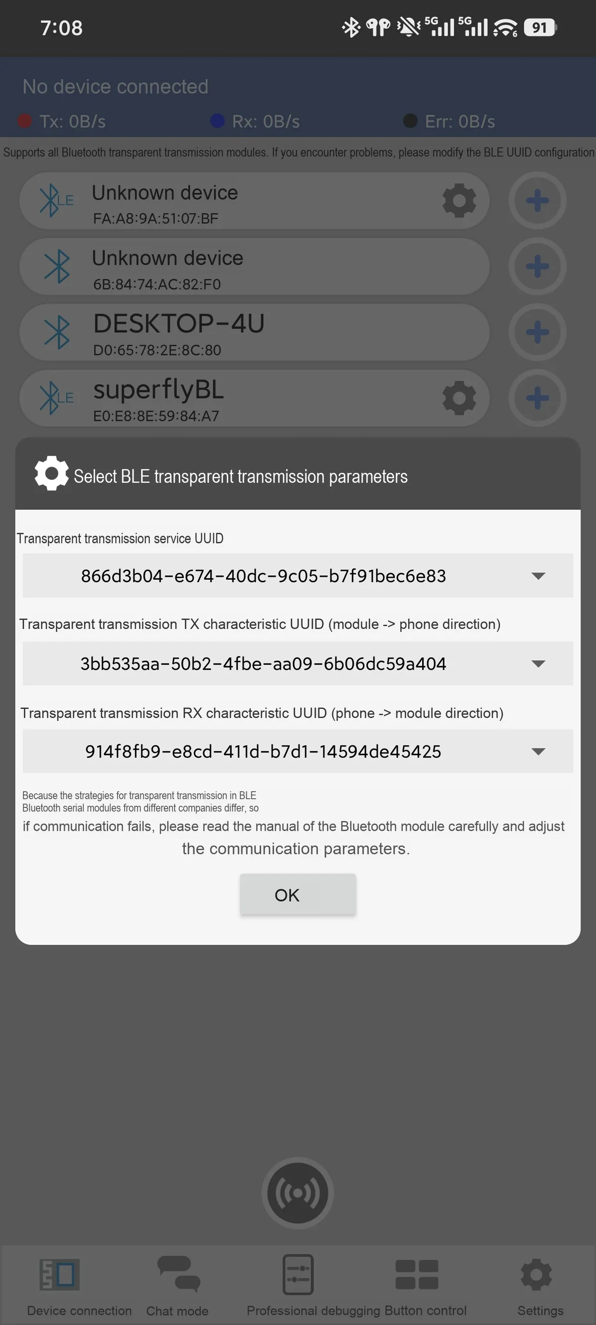
Figure 10: Measured mobile phone configuration. For Service, Transparent TX and Transparent RX, select the UUIDs from the table above respectively. After selection, click "OK" and then connect to the target module.
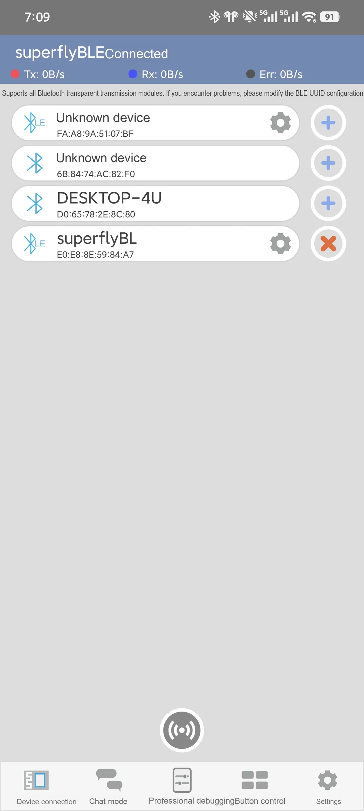
Figure 11: The top of the mobile phone displays "superflyBLE connected". The target address in the screenshot is E0: E8:8E: 59:84: A7, which is consistent with the address converted from the AT return value of the module according to the rule of "lower bits first" specified in the manual.
4.5 Bidirectional Data Transceiver
The test program enables echo via the computer serial port command! echo on. After the mobile phone sends the text 123, the data reaches the main controller along the path "Mobile BLE → DA14531 → UART → RA4M2", then is written back to the module's UART as-is by the RA4M2, and returned to the mobile phone via BLE notification.
The original logs of the main controller are as follows:
[STATUS] baud=115200 connect=1 echo=1 ble_errors=0 ble_lost=0 pc_errors=0 pc_lost=0
[BLE RX HEX] 31 32 33
[BLE RX TXT] 123
[ECHO] Sent received payload back to BLE
31 32 33 are exactly the byte encodings of ASCII text 123. Since the mobile terminal displays the same sent and received content simultaneously, combined with the master control HEX log, it can be confirmed that the short text has completely passed through the bidirectional link.
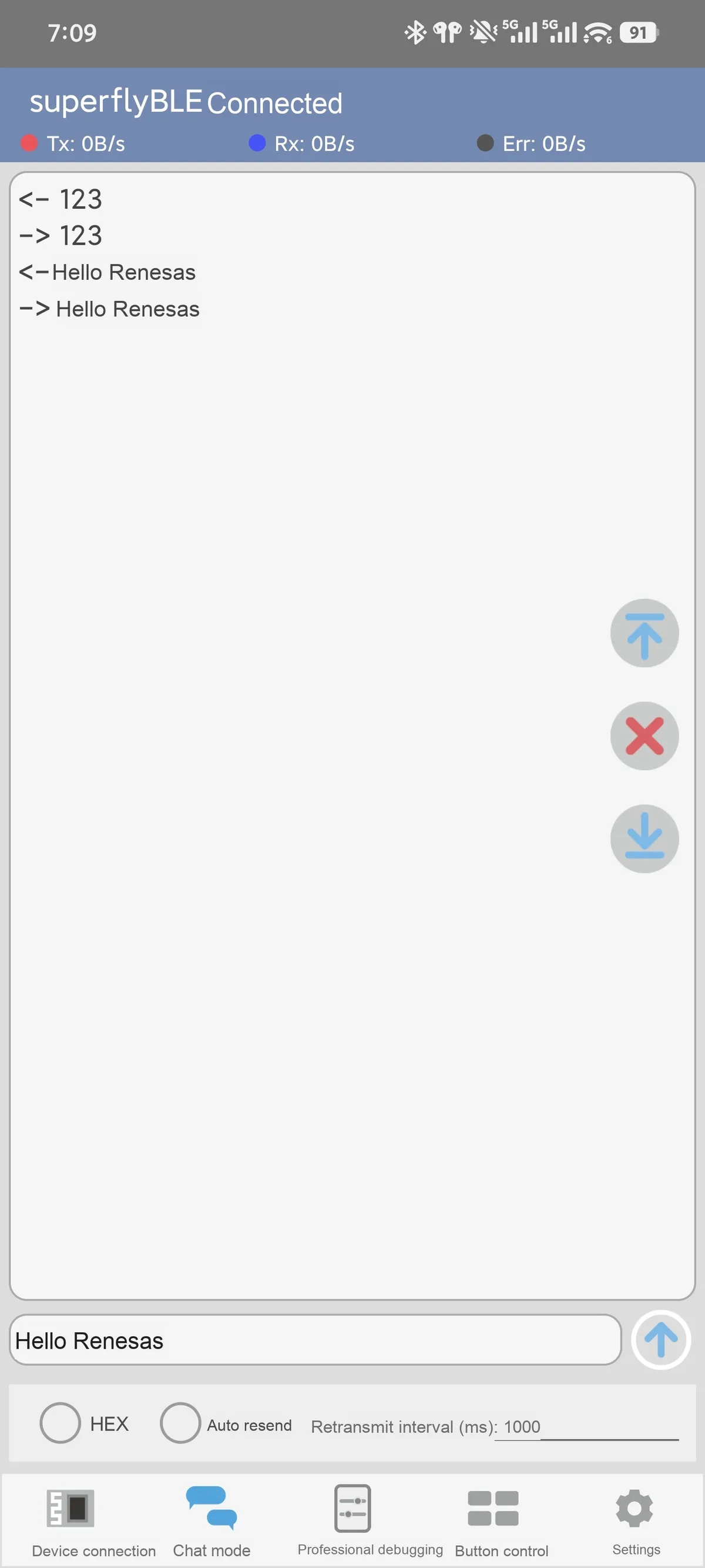
Figure 12: The mobile phone conversation interface displays the sending and return records of two sets of texts, "123" and "Hello Renesas". Among them, "123" has corresponding master control byte logs; the Chinese round-trip communication is confirmed by this mobile phone screenshot and user feedback.
This round verified the short text bidirectional transparent transmission and echo function, and did not conduct tests on continuous throughput, long packet integrity or radio frequency distance. For the original records, please refer to the serial port log of mobile phone sending and receiving test (see the data package at the end of the article); for the original screenshot files and verification information, please refer to the mobile phone creatives records (see the data package at the end of the article).
4.6 Troubleshooting Common Issues
phenomenon | This Experience and Handling |
|---|---|
RFP reports E3000105, the device is unresponsive | After chip identification and before re-writing, keep the SCI/USB BOOT mode, perform a reset, and then connect for programming. |
Burning succeeded but the program did not run | Switch MODE back to INTERNAL FLASH, then press RESET |
AT No response | Check the 3.3V, common ground, TX/RX, reset polarity and LPR; probe at baud rates of 38400 and 115200, with commands terminated by CRLF |
The phone connects but cannot send or receive messages | Check the service UUID, the direction of the Write and Notify characteristics, and enable notifications |
Can't find the baud rate setting on the mobile app | The mobile phone uses BLE; 115200 is the UART parameter between the RA4M2 and the module |
The program fails to start normally after adding a new buffer | Check stack and link allocation; for this v2 release, the main stack has been adjusted from 1KB to 8KB to accommodate the local buffer of the test function |
Chinese characters are displayed as dots in computer logs | The current TXT log only displays printable ASCII characters, with all other bytes shown as dots; cross-check the HEX data against the display on the mobile device, and do not directly conclude that this indicates transmission corruption. |
V. Short Text Transparent Transmission Program and Reproduction
5.1 Organization of the Dual Serial Port Test Program
Dedicated Project RA4M2_DA14531_AT Extended based on the PRINTF project in the resource package: SCI9 acts as the computer Console, and SCI0 is connected to the Bluetooth module. During startup, configure LPR, RESET and CONNECT, detect the module baud rate and query parameters; in the main loop, process computer commands, read module data, output HEX logs, and decide whether to enable echo according to the switch status.
It receives callback-collected bytes, processes the data in the main loop, and waits for a completion event with a timeout set when transmitting. This program uses a ring buffer and reports serial port errors and loss counts. As a short-text joint debugging tool, it has length limits for the receiving window and buffer, and shall not be directly used as a protocol for messages of arbitrary length.
The following is an excerpt of the echo logic for the existing project; the complete source code, SCI0 interrupt configuration, and 8KB main stack settings are all included in the resource package at the end of this document.
bsp_io_level_t connected = BSP_IO_LEVEL_LOW;
(void)R_IOPORT_PinRead(&g_ioport_ctrl, PIN_CONNECTED, &connected);
if (echo_enabled && connected == BSP_IO_LEVEL_HIGH && n &&
    !(n >= 2U && payload[0] == 'A' && payload[1] == 'T'))
{
    (void)ble_send(payload, n);
    log_text("[ECHO] Sent received payload back to BLE\r\n");
}
This demo logic filters data starting with AT to avoid directly echoing the module's response, so it is not applicable to general bridging that requires full transparency of all bytes. For mass production applications, the message boundaries, checksum, queuing and timeout policies shall be defined separately.
5.2 Compile and Serial Port Download
Run the following commands in the root directory of the project to generate the test firmware using the existing build script:
python scripts/build_ble_test.py
The script uses the local GCC 10.3 and the GNU Make path of e² studio; on other computers, the tool paths in the script and build files need to be modified first. Keep the project directory structure intact, use the FSP source code in the resource package, and do not regenerate the FSP configuration. The verified output is modules/DA14531/firmware/RA4M2_DA14531_AT/Debug/RA4M2_DA14531_AT.hex, and this full build has 0 errors and 0 warnings.
Close the serial port assistant, switch the mainboard to SCI/USB BOOT mode and reset it, then download via RFP CLI. The following commands assume that you have navigated to the directory where rfp-cli.exe is located, and have replaced <absolute firmware path> with the actual path of the aforementioned HEX file:
.\rfp-cli.exe -d RA -port COM6 -if uart -s 9600 -range 0,7FFFF -pv "<固件绝对路径>"
The program for RFP V3.25 is located in this project at downloads/rfp-admin/program files/Renesas Electronics/Programming Tools/Renesas Flash Programmer V3.25/. This command involves a program write operation, so please confirm that the target is the current RA4M2.After Operation successful appears, switch back to INTERNAL FLASH and reset, then open the Console with 115200 baud rate, 8 data bits, no parity, 1 stop bit. The firmware for this round has been successfully written and verified.
5.3 Reproduction Steps on Mobile
- Confirm that the main control startup log shows
[PROBE PASS]and[READY], and the actual baud rate of the module is 115200. - When the module is not connected, send the following command from the computer Console:
AT+ ADV= 1; the Console will append CRLF to common AT commands. The module's response in this round isOK+ ADV. - Configure the BLE transparent transmission service of the mobile phone according to the UUID table in Chapter 4, connect to
superflyBLE, and enable Notify; the main controller shall displayconnect= 1. - Enter the following in the computer Console:
! echo onand send it, then confirm thatecho= 1. - Send from the mobile phone in Text mode
123, verify that the mobile phone receives the same text, and check the main controller's31 32 33log. Afterwards, you can use a short Chinese text to test the display function. - When active transmission from the computer is required, enter the following while in the connected state:
! send Hello;! statusto check the status,! echo offto disable echo.
The original AT firmware of the reserved module in this round has not been modified, and no parameter saving or factory reset command has been executed. Recheck the broadcasting and connection status after powering on again. The complete logs and screenshots are available for reference in the material package at the end of the article.
VI. Evaluation Summary
6.1 Completed Validation
Test Item | Results of this round | evidence |
|---|---|---|
LED routine | compile, serial port programming, verification and on-off operation all passed | RFP Logs, Raw Videos and Frame Extraction |
PRINTF Routine | Correctly output integers, floating-point numbers and strings after flashing | Burning and Serial Port Raw Logs |
USRT routine | Compile passed, with 4 warnings | Build record; no physical burning verification performed |
DA14531 AT Command Communication | Response at 115200 baud, 7 parameter queries completed | Start Raw Bytes and Parsing Results |
Mobile Phone Connection | Scanned and connected to superflyBLE | Screenshot of Mobile Phone and CONNECT Status |
Bidirectional Transparent Transmission for Short Texts | Successful round-trip display of numbers and Chinese characters | Digital master control HEX logs, mobile phone screenshots |
The test was completed on November 6,2026. This round is positioned as a basic function evaluation, and does not cover continuous throughput, long packet integrity, communication distance, formal disconnection and reconnection stability, or current, so no conclusions will be drawn on these metrics.
6.2 Hardware Connection and Development Experience
Pmod integrates the power supply, UART and control lines into a single interface, reducing the need for jumper wires; the onboard CH340 enables microcontroller programming and log monitoring to be completed in stages via the same serial port interface. Starting with LED and PRINTF debugging before introducing the Bluetooth module helps verify the motherboard operation, computer serial port and BLE link layer by layer.
When getting started, the most common factors that easily hinder progress include mismatched versions between reference materials and physical hardware, absolute paths of old projects retained on the original author's computer, and the inverted reset signal of the Pmod baseboard. This article corrects the paths via a working copy, preserves the original examples, and documents the actual compile and wiring schemes.
6.3 Selection of AT Firmware and Secondary Development
The factory default AT firmware already supports query, advertising, connection and data pass-through for this release, and the RA4M2 application does not need to directly implement the BLE protocol stack. On the mobile phone side, you still need to correctly select the service, write the characteristic and enable the notification characteristic; it is not a classic Bluetooth serial port that can be used without configuration.
If the primary requirement of the project is a small amount of status data and control messages, the AT solution can be adopted first to verify the application. When it is necessary to customize GATT, broadcast logic or develop independent low-power applications, you can then proceed to SmartBond SDK6 and adapt the pins and storage according to the circuit of this module. This secondary development route has not been implemented in this round.
6.4 Comprehensive Evaluation
The combination of RA4M2 and DA14531 this time has completed a complete functional chain covering source code compile, serial port download, and short text transmission between the device and mobile phone, making it suitable as an entry-level prototype for MCUs to add BLE communication. The existing screenshots, serial port logs, and compilable source code are sufficient to support the conclusions of this article; if it is to be used in continuous collection or battery-powered products in the future, special verification will be carried out around the actual message length, transmission rhythm, and power supply method.
References
All reference materials and test attachments are collectively provided in the ZIP file below. It contains two original vendor ZIP files (for motherboard documentation and DA14531 documentation, with original filenames and content retained), this Markdown document, dedicated test project and compile scripts, original on-site photos and LED videos, mobile phone screenshots, build and flashing records, as well as AT and transmission-reception logs. The archive-inventory.json inside the package lists the file paths, sizes and SHA-256 values; DA16200 documentation or tool installation packages are not included.
DA14531-review-materials-v1.0.1.zip 62.8 MB
- Reference Article for RA6M4 Development Board Evaluation: Reuse the six-chapter structure, common interfaces and installation creatives; Figure 6 and Figure 7 are sourced from this article.
- Renesas DA14531 Official Product Documentation: Chip Resources and BLE Positioning.
- FSP 6.6.0 Official Release Page: Integrated installation package.
- Official Getting Started Guide for SmartBond SDK6: Reference for subsequent chip application development.
Version Record
Version Number | Revision Date | Modifier | Modify Content |
|---|---|---|---|
v1.0 | 2026-11-06 | Zhao Yansong | Create a standardized version, summarize the completed actual measurements of the motherboard and BLE, and organize the images, source code and reference attachments |
v1.0.1 | 2026-11-06 | Zhao Yansong | Complete the schematic diagram of the PMOD interface, add three new real photos of hardware details, adjust the figure numbers, and update the data package |