
Contents
- 1. Unboxing of Development Board and Hardware Overview
- 1.1 Overall Appearance of the Development Board
- 1.2 Distribution of Onboard Core Components and Interfaces
- 1.3 Power Input and Type-C Port
- 1.4 Key, LED and Touch Key Resources
- 1.5 Description of PMOD, SWD and Expansion Interfaces
- 2. Analysis of RA6M4 Main Control Resources and On-Board Circuits
- 2.1 Overview of RA6M4 Main Control Chip
- 2.2 Key Parameters of R7FA6M4AF3CFP
- 2.3 Cortex-M33, TrustZone and Security Features
- 2.4 Memory Resources and Peripheral Resources
- 2.5 Analysis of CH340 Serial Port Download Circuit
- 2.6 Analysis of SWD Debug Interface Circuit
- 3. Development Environment Setup and Project Preparation
- 3.1 Composition of Development Environment
- 3.2 Installation of e² studio and FSP
- 3.3 Installation of CH340 Serial Port Driver
- 3.4 Renesas Flash Programmer Installation
- 3.5 Prepare the project directory
- 3.6 Description of Sample Project Directory
- 3.7 Import the RA6M4_LED Project
- 3.8 Check FSP Configuration
- 3.9 Compile the project and generate the hex file
- 4. Program Download and Basic Experiment Verification
- 4.1 Description of Download Methods
- 4.2 CH340 Type-C and SCI Boot Download Process
- 4.3 Renesas Flash Programmer Connection Settings
- 4.4 Flash RA6M4_LED.hex
- 4.5 Switch back to Internal Flash and reset for operation
- 4.6 LED Blink Experimental Phenomenon
- 4.7 Serial Port Printing Experiment Verification
- 4.8 Troubleshooting Download Failures
- 5. Quick Start Lab
- 5.1 Sample Project Resources
- 5.2 ToF Ranging Application
- 6. Evaluation Summary
- 6.1 Summary of hardware Resources
- 6.2 Software Ecosystem and FSP Usage Experience
- 6.3 Experience of CH340 Download Method
- 6.4 Suggestions for SWD Debugging Extension
- 6.5 Application Scenarios and Comprehensive Evaluation
- References
1. Unboxing of Development Board and Hardware Overview
1.1 Overall Appearance of the Development Board
From a practical evaluation perspective, this type of 100-pin development board has the advantage of achieving a favorable balance between the number of interfaces and on-board resources. Compared with smaller minimal system boards, it directly provides buttons, LEDs, UART, debug ports and expansion ports; compared with highly complex evaluation kits, it maintains a lower barrier to entry. For developers who are new to the Renesas RA series, after getting the board, they can start with LED, UART and FSP configuration, and then gradually expand to ADC, PWM, touch buttons and external Flash.
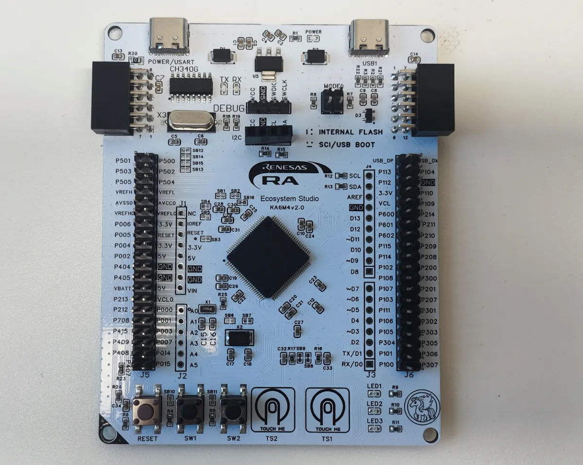
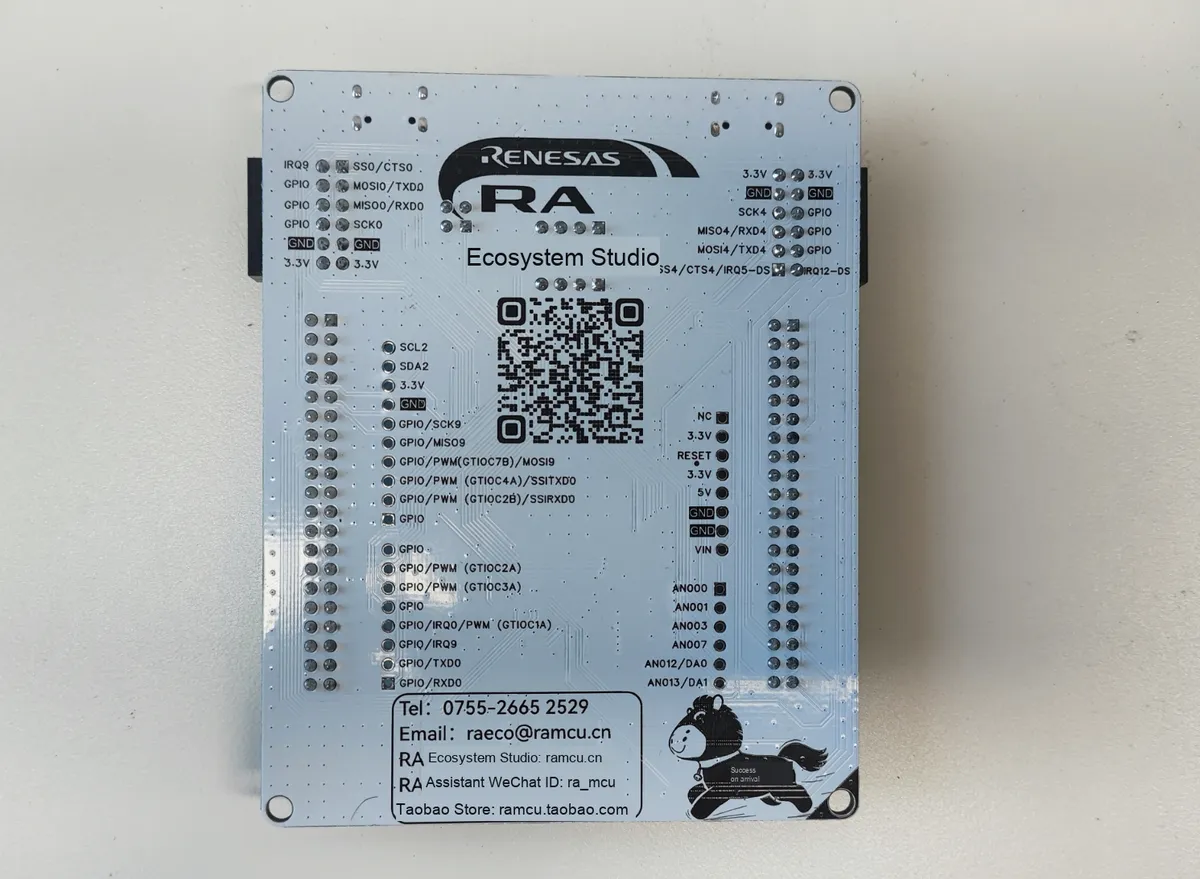
On the front side of the board, the layout centers on the RA6M4 main control chip, with download, debugging and expansion interfaces arranged around it. This layout facilitates simultaneous connection of Type-C cables, serial port tools, oscilloscope probes and peripheral modules during experiments. In practical use, the LED and button resources are placed in positions that are easy to observe and operate, enabling quick judgment on whether the program is running properly.
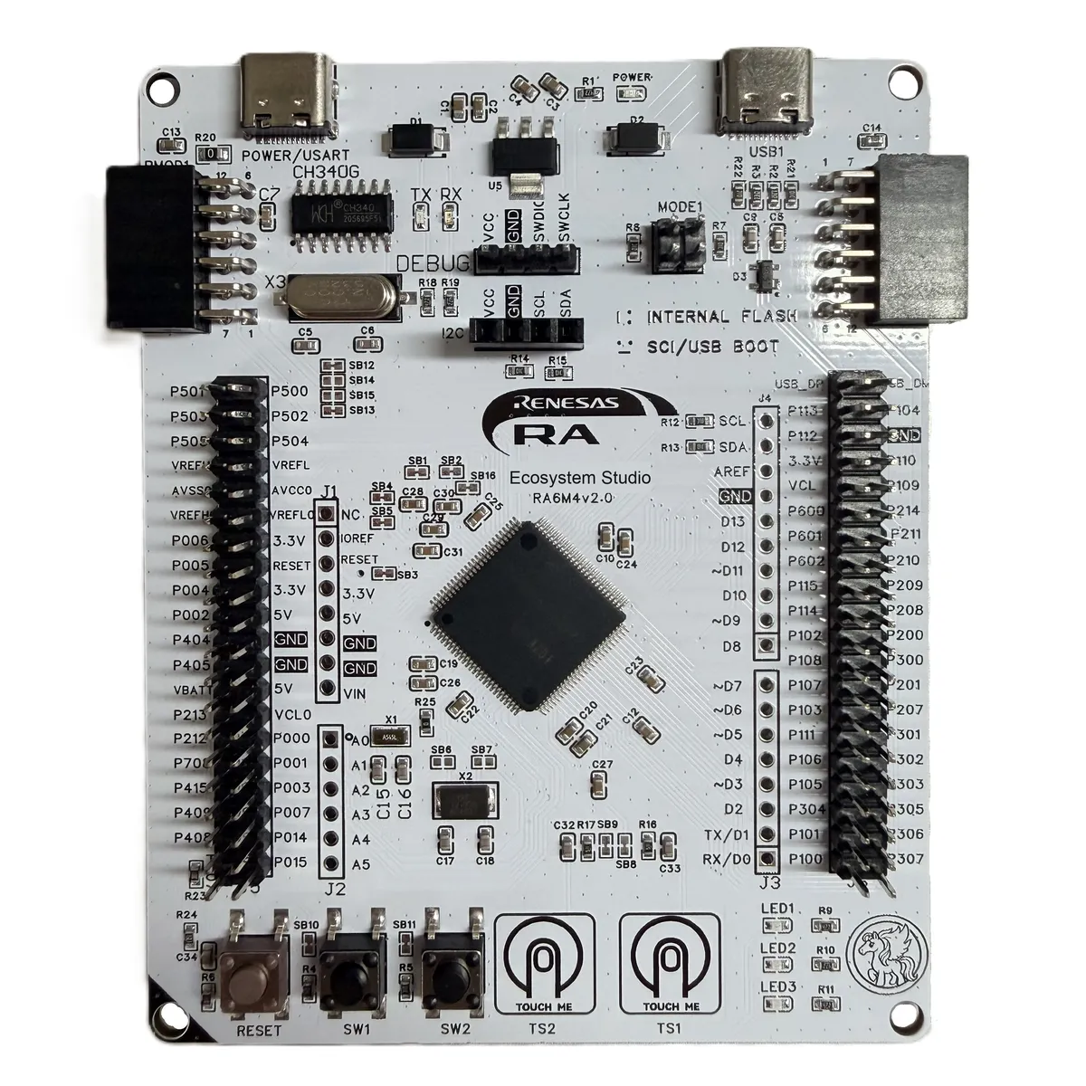
The RA-Eco-RA6M4-100PIN-V2.0 development board uses a 100-pin RA6M4 main control chip as the core controller, and integrates common resources on board such as a Type-C serial port interface, SWD debug interface, PMOD expansion interface, user buttons, touch buttons and LEDs. The board features a clear overall layout, with the core chip, download interface and expansion interfaces all positioned at locations convenient for wiring and observation, making it suitable for RA6M4 beginner learning, peripheral verification and small-scale prototype development.
1.2 Distribution of Onboard Core Components and Interfaces
The distribution of core components and interfaces is an important criterion for evaluating whether a development board is suitable for learning and project verification. This board integrates resources such as MCU, CH340, SWD, PMOD, buttons and LEDs on a single board, which can serve not only as a basic teaching platform for microcontrollers, but also as a verification platform for peripheral drivers. For MCUs with relatively rich resources like the RA6M4, the value of onboard expansion interfaces is quite prominent, as it allows developers to complete various peripheral experiments without having to redesign a base board.
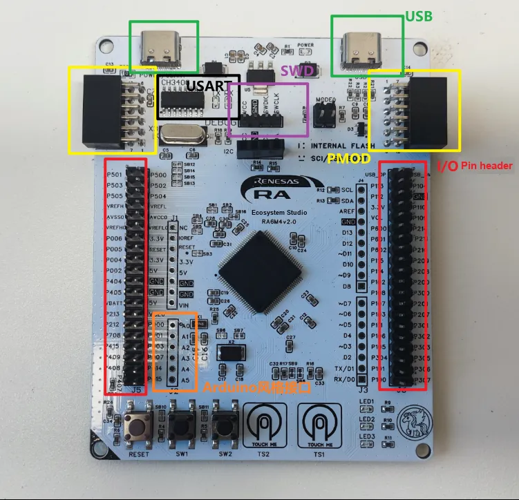
Regarding the sequence of using the interfaces, it is recommended to first use the onboard CH340 to complete serial port identification and basic programming, then use the LED project to confirm the program operation, and finally connect sensors, OLED or oscilloscopes according to experimental requirements. This allows separate troubleshooting of environment issues, download issues and application issues, thus reducing debugging complexity.
In terms of board resources, the development board leads out common communication interfaces and debug download interfaces around the RA6M4 main control. The Type-C interface is connected to the onboard CH340, which can be used for serial communication and SCI Boot programming; the SWD interface is used to connect debuggers such as J-Link, Renesas E2 Lite or CMSIS-DAP; the PMOD interface is used to expand sensors, display modules or other peripherals.
- Main control area: The core component is R7FA6M4AF3CFP, with a 100-pin package.
- Download and Communication Area: Onboard CH340 Type-C interface, which can be recognized as a COM port on the computer side.
- Debug Area: On-board SWD interface for convenient in-circuit debugging.
- Interaction area: consists of a reset button, user buttons, touch buttons, and 3 LEDs.
- Expansion Area: Includes expansion interfaces such as PMOD to facilitate the connection of peripheral modules.
1.3 Power Input and Type-C Port
The Type-C interface plays a very critical role in this evaluation. It not only provides a convenient connection method between the board and the computer, but also enumerates a serial port device in the system via the CH340. When downloading a program using the Renesas Flash Programmer, the RFP actually communicates with the Boot ROM of the RA6M4 through this serial port. Therefore, the Type-C cable used must support data transmission, and a cable that only supports charging cannot be used.
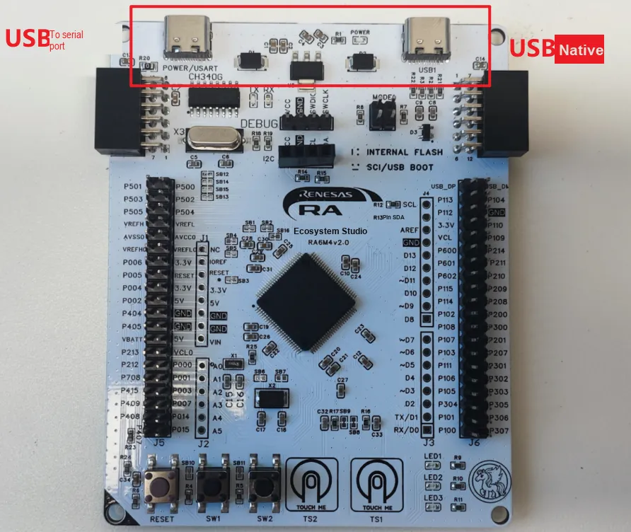
Power supply stability directly affects the downloading and running results. If "device is not responding", connection interruption or verification failure occurs during the RFP connection process, priority should be given to checking the status of the power supply, cables and COM port. When conducting ADC, DAC or external module experiments, it is also necessary to pay attention to whether the power supply of the peripheral matches the level of the development board.
After the development board is connected to a computer via the Type-C interface, the onboard CH340 is responsible for converting between USB and serial port signals. This interface serves two purposes in this evaluation: first, it acts as a serial communication channel; second, it cooperates with the Renesas Flash Programmer to complete program burning after the chip enters the SCI Boot mode.
1.4 Key, LED and Touch Key Resources
LEDs are the most intuitive verification resource in embedded development. They can be used to confirm whether GPIO output, delay function, clock initialization, FSP-generated code and Flash programming process work properly. User buttons are suitable for verifying external input, level reading and interrupt triggering. Compared with ordinary mechanical buttons, touch buttons have an additional layer of capacitive touch detection logic, making them more suitable for demonstrating the peripheral capabilities of the RA6M4 in human-computer interaction.
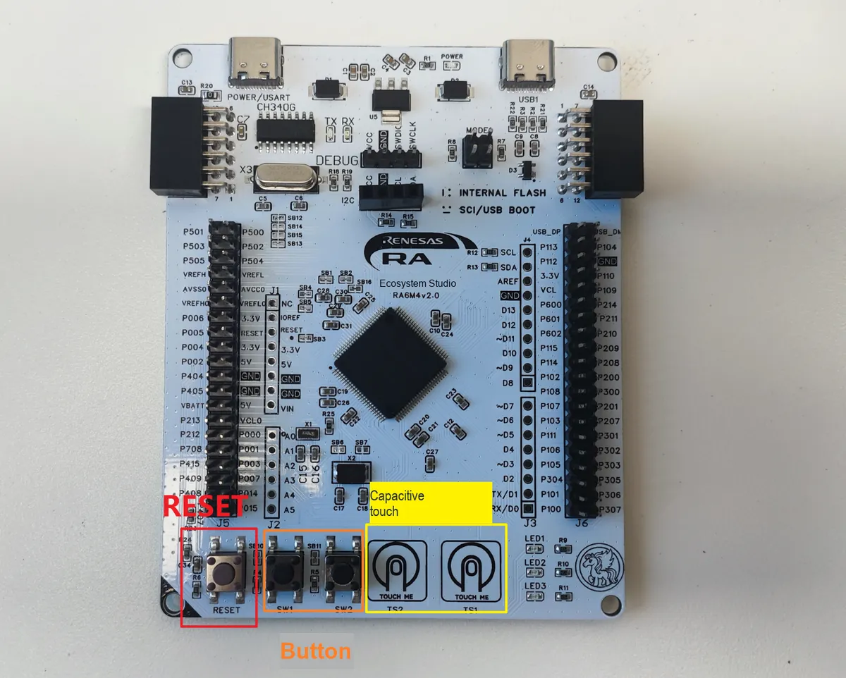
In the formal evaluation, LED Blink is not just a simple LED blinking experiment, but a closed-loop verification of the entire development process: correct project import, correct FSP configuration, correct compile output, correct RFP programming, correct switchback of Boot mode, and only then can a stable LED blinking phenomenon be observed.
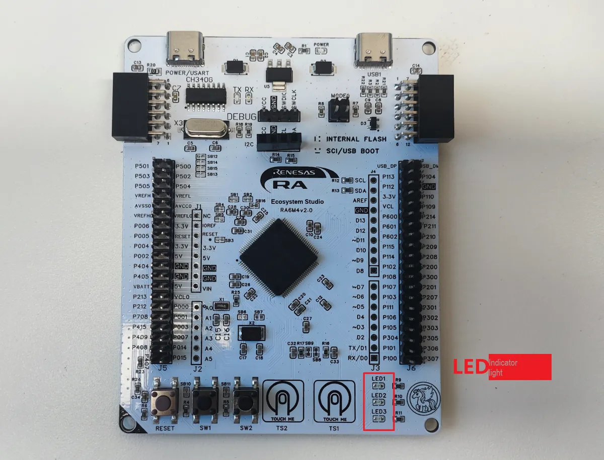
The development board is equipped with 2 user keys, 2 touch keys and 3 LEDs. The LED resource is suitable as the first basic experiment to verify whether the processes of project import, FSP configuration, compile, programming and program running are complete. The touch keys can be used for extended verification in combination with the built-in capacitive touch unit of the RA6M4.
1.5 Description of PMOD, SWD and Expansion Interfaces
The PMOD interface makes the development board more suitable for Modularization expansion, such as connecting OLED displays, environmental sensors, external storage or wireless communication modules. Since the PMOD interface usually includes power supply, ground and several communication pins, it is necessary to confirm the specific pin multiplexing relationship in combination with the schematic diagram during experiments to avoid conflicts with onboard resources.
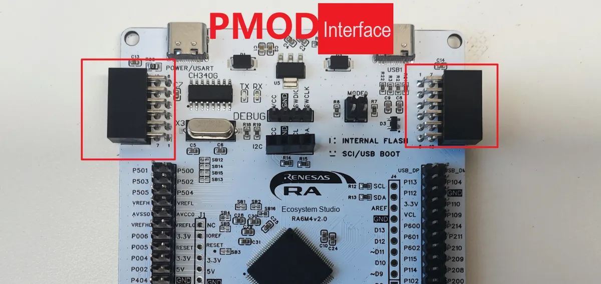
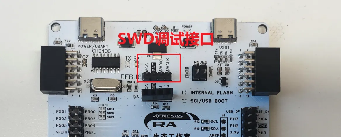
The SWD interface is a critically important interface for in-depth development. Although this basic evaluation uses the CH340 + SCI Boot for program downloading, the SWD debugger can significantly improve efficiency when analyzing complex peripherals, locating HardFaults, checking variable statuses, or debugging interrupt logic.
The PMOD interface facilitates the expansion of external modules, and can be connected to OLEDs, sensors, Flash or other communication modules. The SWD interface retains full on-line debugging capabilities; when breakpoints, single-step execution, variable observation and register viewing are required, debuggers such as J-Link, Renesas E2 Lite or CMSIS-DAP can be used for connection.
2. Analysis of RA6M4 Main Control Resources and On-Board Circuits
2.1 Overview of RA6M4 Main Control Chip
The RA6M4 is a high-performance MCU in the Renesas RA product family, positioned between general-purpose control and high-performance secure connectivity applications. Featuring a Cortex-M33 core that delivers a high operating frequency and modern Armv8-M architecture attributes, it, paired with the Renesas FSP, can address development requirements ranging from bare-metal control to RTOS-based applications.
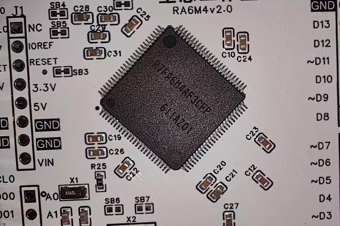
From the perspective of development board evaluation, the value of the RA6M4 lies not only in its main frequency and Flash capacity, but also in that it provides rich connectivity interfaces, security capabilities, and analog/timing peripherals at the same time. This means that the same development board can not only complete basic GPIO experiments, but also be extended to applications involving networking, USB, encryption, touch control and multi-peripheral collaboration.
The RA6M4 series MCUs adopt the Arm Cortex-M33 core, support TrustZone, and integrate security-related capabilities such as the Secure Crypto Engine. Compared with the RA4 series, the RA6M4 is more suitable for applications requiring higher performance and connectivity in terms of main frequency, storage resources, network interfaces and security features.
2.2 Key Parameters of R7FA6M4AF3CFP
The resource configuration of the R7FA6M4AF3CFP is quite user-friendly for both learning and project verification. Its 1 MB Code Flash can accommodate relatively complete applications and Middleware, while the larger SRAM space is better suited for running Communication Protocol stacks, display buffers or complex data processing logic. The 100-pin package allows more peripheral signals to be routed out to the development board, facilitating practical connection and testing.
When selecting a sample project or porting an existing project, it is mandatory to verify that the target device specified in the BSP matches the physical hardware. In this session, we read the chip signature via the RFP to confirm that the actual device is R7FA6M4AF3CFP, which is critical for FSP configuration, linker scripts, Flash programming algorithms, and proper program execution.
Project | Parameters |
Device Model | R7FA6M4AF3CFP |
CPU core | Arm Cortex-M33 |
Maximum Boost Clock | 200 MHz |
Code Flash | 1 MB |
SRAM | 192 KB SRAM + 64 KB ECC SRAM |
Data Flash | 8 KB |
Encapsulation | 100 pins |
Security Capability | TrustZone, Secure Crypto Engine |
Typical Peripherals | Ethernet MAC, USB FS, CAN, SCI, SPI, I2C, QSPI, OctaSPI, SDHI/MMC, ADC, DAC, GPT, AGT, capacitive touch unit |
2.3 Cortex-M33, TrustZone and Security Features
TrustZone is a key feature that distinguishes the RA6M4 from many traditional Cortex-M4 MCUs. It allows developers to place critical code, keys and security services in the Secure region, and put ordinary application logic in the Non-secure region. For products requiring firmware protection, identity authentication, encrypted communication or secure upgrades, such hardware isolation capabilities are of practical significance.
In the introductory experiment phase, you can skip enabling complex security isolation first, and use a common bare-metal project to complete GPIO and UART tests. After the basic workflow stabilizes, you can then gradually explore Secure/Non-secure projects, key injection, secure boot, and encrypted peripherals.
Compared with the traditional Cortex-M4, the Cortex-M33 core adds TrustZone support for security isolation, which can divide the system into Secure and Non-secure regions. The security features of the RA6M4 are suitable for IoT gateways, industrial control terminals, and scenarios requiring firmware protection, key management or secure communication.
2.4 Memory Resources and Peripheral Resources
The RA6M4 features a wide coverage of peripheral resources, making it suitable for conducting multiple types of experiments consecutively with a single development board. The SCI can be used for UART, simple SPI and simple I2C; the GPT and AGT can be applied to PWM, timer interrupts and periodic tasks; the ADC and DAC are capable of analog input and output; while USB, CAN and Ethernet are designed for connectivity-oriented applications.
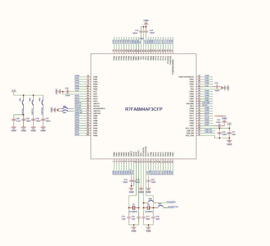
This combination of resources enables the development board to not only demonstrate individual peripherals, but also be combined into applications closer to the Product Form, such as sensor data acquisition followed by output via serial port or network, PWM-controlled actuators, and parameter storage in Flash at the same time.
The RA6M4 integrates 1 MB Code Flash, data Flash and a large-capacity SRAM, which can accommodate relatively complex Middleware and application logic. In terms of peripherals, the chip provides resources such as Ethernet, USB, CAN, SCI, SPI, I2C, timers, ADC, DAC and capacitive touch, covering the requirements of general control, human-machine interaction, sensor acquisition and network communication.
2.5 Analysis of CH340 Serial Port Download Circuit
The CH340 features mature drivers, ease of use, and relatively low cost. With the CH340 onboard, users can perform serial communication and Boot programming without additionally preparing a USB-to-TTL module. The fact that RFP can read the chip signature via the COM port indicates that the serial download link, Boot mode, and target chip response of the development board are all functioning properly.
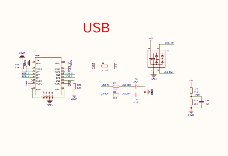
It should be noted that the CH340 is only a serial port bridge chip, not a debugger. It can assist in program flashing and printf output, but cannot replace the J-Link for breakpoint debugging. The document separately explains these two types of tools to avoid confusing "downloading" with "debugging".
The onboard CH340 converts USB signals to TTL serial port signals. After the chip enters the SCI Boot mode, the Renesas Flash Programmer on the computer can establish a connection with the RA6M4 Boot ROM through this serial port. During the actual connection process, RFP can read the chip signature information via the COM port and identify the target device as R7FA6M4AF3CFP.
2.6 Analysis of SWD Debug Interface Circuit
The SWD debug interface is typically used for in-depth troubleshooting during the development phase. Via SWD, a debugger can control the CPU to halt, execute step-by-step, read registers, set breakpoints, and inspect memory. For complex peripheral driver and interrupt issues, the debugging efficiency of SWD is far higher than that of simple serial port printing.
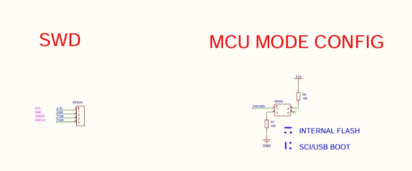
This evaluation retains the SWD description because it is a standard capability of the RA6M4 development board. Even if the current experiment uses the CH340 for downloading, it is still recommended to connect an SWD debugger when debugging TrustZone, USB, Ethernet, or RTOS applications.
The SWD interface generally includes signals such as SWDIO, SWCLK, GND, VCC reference voltage, and NRST. This interface is used to connect a dedicated debugger, enabling programming and debugging within the e² studio environment. Compared with the CH340 serial port programming method, the advantage of SWD is that it supports in-circuit debugging.
3. Development Environment Setup and Project Preparation
3.1 Composition of Development Environment
The RA series Development Environment features a large number of toolchain components with clear division of responsibilities: e² studio is in charge of engineering management and compile, FSP takes charge of graphical configuration and driver generation, Renesas Flash Programmer is responsible for standalone programming, and the CH340 driver handles serial port recognition. Sorting out the relationships between these tools will give you clearer direction when troubleshooting issues.
| Tool/Software | Purpose |
|---|---|
| e² studio | Renesas official integrated development environment, used for project import, configuration, compilation and debugging |
| Renesas FSP | RA series software package, providing BSP, HAL drivers, middleware and code generation |
| Renesas Flash Programmer | RA series serial download program |
| Arm GNU Toolchain | Compiles C/C++ projects; usually installed together with the e² studio/FSP installer |
| CH340 serial port driver | Recognizes the on-board USB-to-serial chip of the development board, used for serial printing and communication |
| Serial debugging assistant | View printf output and UART transmit/receive data |
| SWD debugger | Used for program download, single-step debugging, breakpoint debugging and variable inspection |
The process adopted in this evaluation is to first complete project import and compile in e² studio, then use RFP to perform serial port Boot programming. This method is more suitable for the current usage scenario where only the onboard CH340 is available and there is no dedicated SWD debugger.
This evaluation uses e² studio as the Integrated Development Environment, FSP as the underlying driver and configuration framework, and Renesas Flash Programmer as the serial port Boot programming tool. The onboard CH340 Type-C interface is responsible for providing the serial communication channel.
3.2 Installation of e² studio and FSP
It is recommended to directly select the integrated installation package containing FSP when installing e² studio. In this way, you can obtain the IDE, FSP package, compile toolchain and necessary plugins at the same time, reducing version mismatch issues. After the installation is complete, if a FSP version difference is prompted during project import, you can perform configuration upgrade or keep the original version of the sample project according to the IDE prompts.
FSP serves as a core layer in the development of the RA series. It not only generates initialization code, but also integrates chips, clocks, pins and peripheral drivers through the configuration interface. For beginners, learning to open configuration.xml and check the BSP and Pins pages first is the foundation of using the RA series.
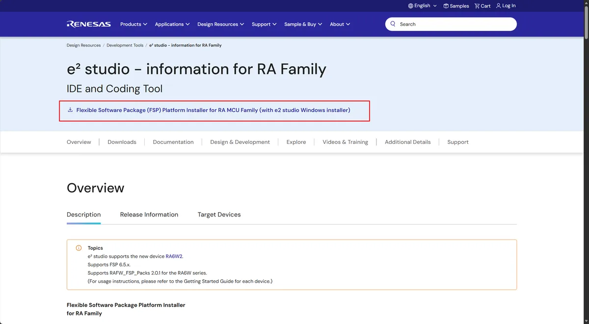
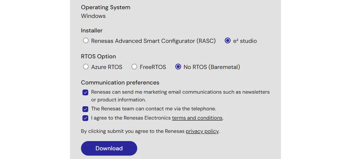
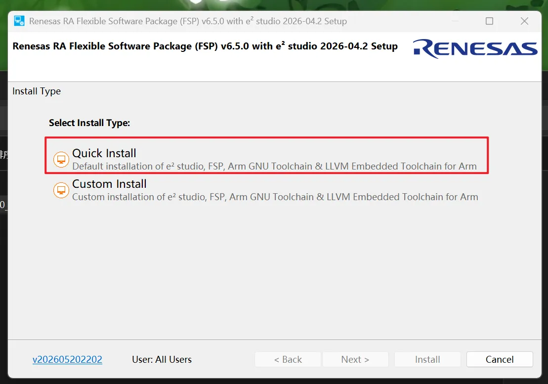
When installing e² studio, select the installation package that integrates FSP. For the installation type, you can choose Quick Install to install the IDE, FSP, Arm GNU Toolchain, and LLVM Embedded Toolchain for Arm in one go. The RTOS option can be selected according to the experimental requirements, and this basic experiment adopts the Baremetal approach.
- Open the official Renesas download page and select the e² studio installation package.
- For RTOS Option, select No RTOS (Baremetal).
- Run the installer and select Quick Install.
- After the installation is complete, launch e² studio and create a new or select an existing workspace.
- Confirm that the GNU ARM Embedded toolchain is available in Toolchain Management.
3.3 Installation of CH340 Serial Port Driver
After the CH340 driver is installed, when the development board is connected to a computer, a new COM port will appear in the Device Manager. This COM port can be used by RFP for SCI Boot download, and can also be used by the serial port assistant to view program prints. During the experiment, note that the same COM port cannot be occupied by multiple software at the same time, otherwise RFP may fail to connect.
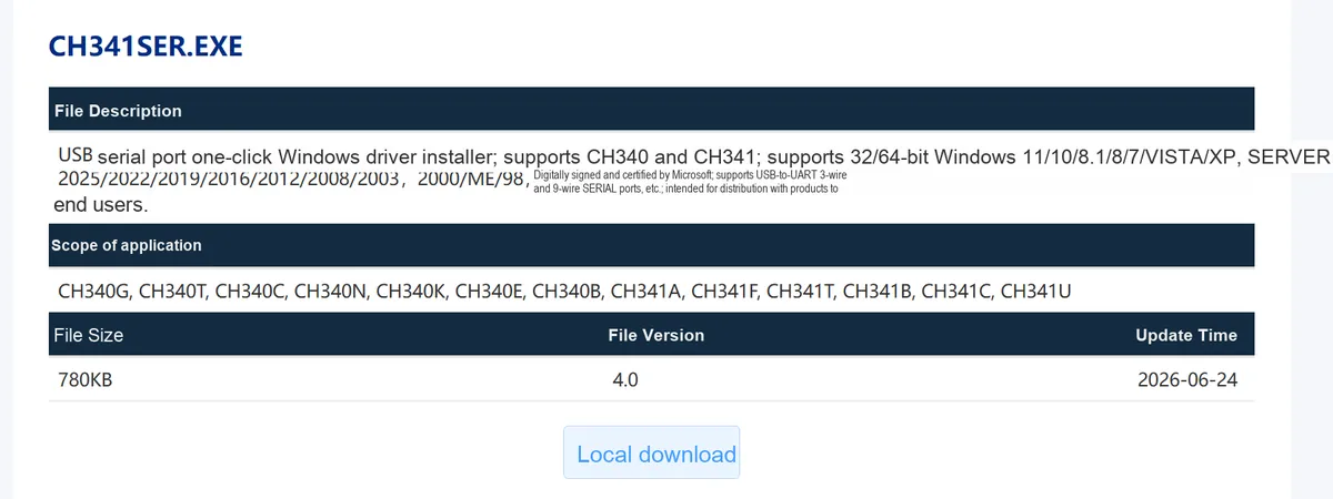
If no COM port appears after inserting the development board, you can troubleshoot from the aspects of cable, driver, USB port and board power supply. Using a charging-only cable is one of the common issues.
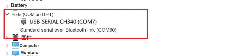
After connecting the Type-C interface of the development board, the corresponding COM port should appear in the Windows Device Manager. If it is not recognized, you need to install the CH340 driver. After the driver is installed, reconnect the development board and confirm that the Port Number appears stably.
3.4 Renesas Flash Programmer Installation
Renesas Flash Programmer is an official programming tool from Renesas, designed to complete program flashing without online debugging. It supports connecting to the target chip via UART Boot, USB Boot, and some debugger interfaces. For this development board, the most straightforward method is to select RA + COM port and establish a connection through the onboard CH340.
When installing RFP, keep the relevant USB Boot and Renesas MCU Tools drivers, which can avoid reinstalling components when switching to other download methods. After the installation is complete, it is recommended to create a test project first to confirm that the software can correctly identify the COM port and the target chip.
Since this evaluation uses the CH340 Type-C interface for SCI Boot programming, it is necessary to install the Renesas Flash Programmer. During installation, check the main program of Renesas Flash Programmer, and install the Renesas MCU Tools and USB Boot-related drivers.
- Open the official Renesas website and download the Windows installer package for Renesas Flash Programmer.
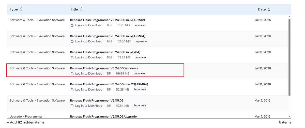
- Run the installer and check the main program of Renesas Flash Programmer.
- Retain the driver options related to Renesas MCU Tools, E1/E20 emulator and USB Boot.
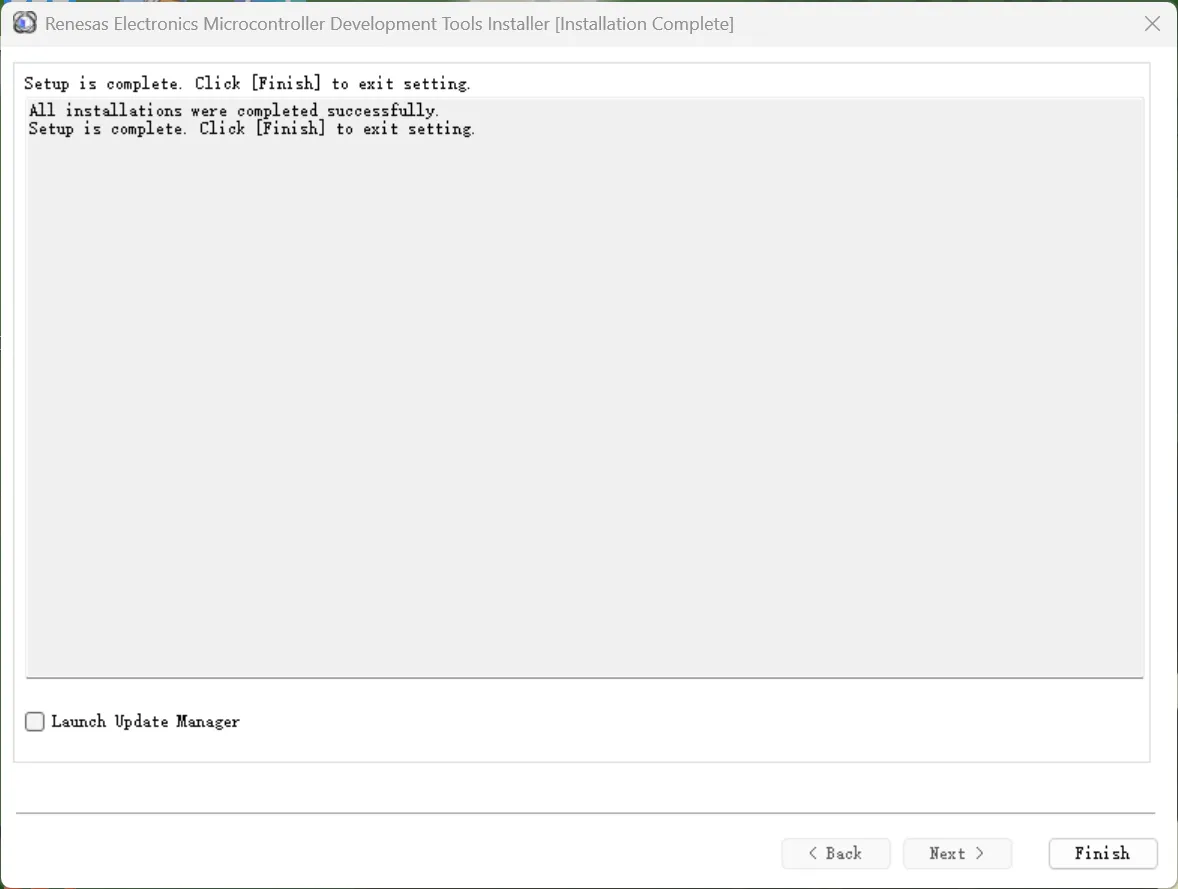
- After the installation is complete, start Renesas Flash Programmer from the Start menu.
- Create a new RA project and select the COM port as the communication tool.
3.5 Prepare the project directory
The sample projects in the resource package are highly sensitive to paths. It is not recommended to use Chinese paths when importing the sample routines. To avoid exceptions during path parsing by e² studio, compilers or script tools, it is advised to copy the materials to a directory with a pure English path.
The recommended directory structure is as follows:
D:\RA6M4_Workspace
├─ RA6M4_100PIN_example
│  ├─ RA6M4LED
│  ├─ RA6M4PRINTF
│  ├─ RA6M4GPIOINPUT
│  ├─ RA6M4ADC
│  ├─ RA6M4DAC
│  └─ ...
└─ e2studio_ws
Wherein:
RA6M4_100PIN_exampleis used to store the example programs for the development board.e2studio_wsServes as the workspace for e² studio.- Do not include Chinese characters, spaces or special symbols in the path.
For example, the following is not recommended:
D:\瑞萨开发板\RA6M4例程Recommended:
D:\RA6M4_Workspace\RA6M4_100PIN_example3.6 Description of Sample Project Directory
The example projects provided in the resource package cover most introductory scenarios ranging from basic GPIO to common peripherals. This organization of materials is extremely user-friendly for evaluation, as you can first set up a flashing closed loop with the LED project, then verify the serial port with the PRINTF project, and finally expand with projects such as ADC, PWM, DAC, touch, and OLED.
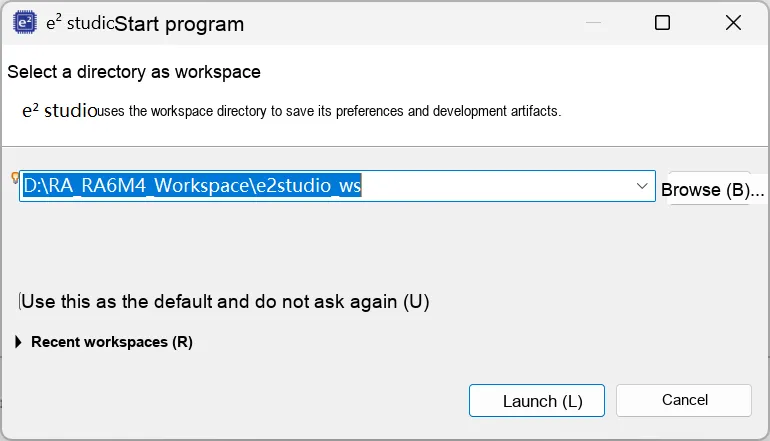
Each example project contains configuration.xml and the FSP generation directory. When evaluating these projects, you should not only check the source code but also review the FSP configuration, as many peripheral instances, pin multiplexing and clock selections are specified in the configuration file.
The example project in the resource package is located in the RA6M4_100PIN_example directory, which covers common experiments such as LED, PRINTF, ADC, DAC, PWM, touch keys, RTC, OLED, W25Q128, and watchdog.
3.7 Import the RA6M4_LED Project
When importing a project, it is recommended to use the existing project import method instead of manually copying the source code after creating a new empty project. This way, the original FSP configuration, linker script, startup files and project properties can be retained. If there are any abnormalities with the project name, path or toolchain after import, you can first execute Clean Project and then rebuild it.
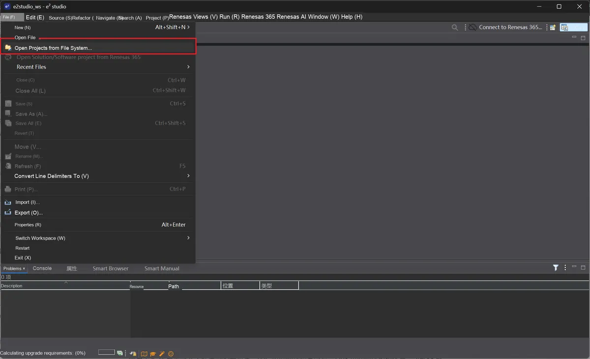
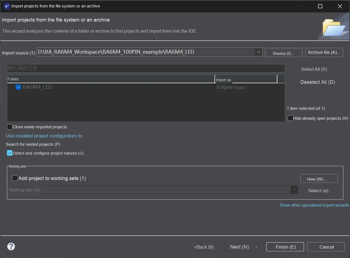
RA6M4_LED is the most suitable project for the first verification. It requires few resources and delivers intuitive observable results; even without serial port output, you can determine whether the program is running properly by checking the status of the LED.
In e² studio, select **Import Existing Projects** and set the project root directory to the `RA6M4_LED` folder in the resource package. Once the import is complete, you will see directories such as `configuration.xml`, `src`, `ra`, `ra_cfg`, `ra_gen`, `script`, and `Debug` in the Project Explorer.
3.8 Check FSP Configuration
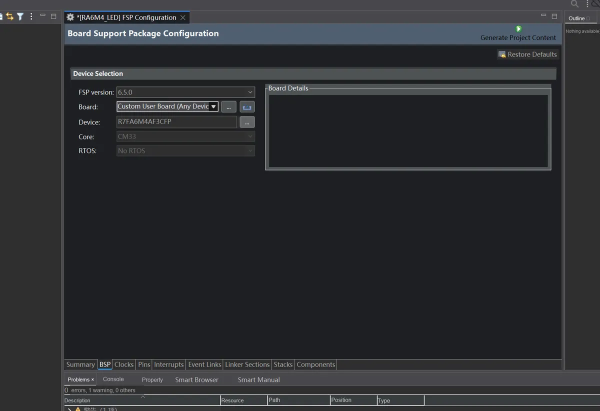
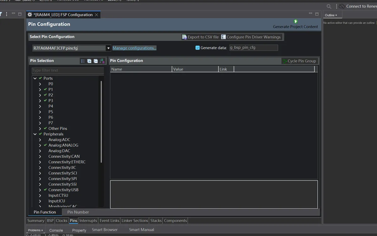
Checking the FSP configuration is a necessary step after importing a project. Confirm the chip model on the BSP page, verify the pin configuration on the Pins page, and check the driver modules in use on the Stacks or Components page. For RA6M4 projects, the target device must match the physical hardware; otherwise, a situation may occur where the compile succeeds but downloading or running the device malfunctions.
In this actual measurement, the chip signature read by the RFP is R7FA6M4AF3CFP, so the documents, projects and download tools should all be unified to RA6M4. This confirmation process also shows that when writing evaluation documents, one should not only rely on folder names or old document names, but take the physical silk screen and tool identification results as the standard.
Double-click configuration.xml to open FSP Configuration. On the BSP page, the target device should be R7FA6M4AF3CFP, the CPU series is RA6M4, and the RTOS is configured as None. On the Pins page, the selected pin configuration file is R7FA6M4AF3CFP.pincfg.
- Double-click configuration.xml in the project.
- Go to the Summary or BSP page and confirm that the target chip is R7FA6M4AF3CFP.
- Go to the Pins page and confirm that R7FA6M4AF3CFP.pincfg is used.
- Check the pin configurations of components such as LEDs, serial ports, and buttons.
- Click Generate Project Content to regenerate the FSP code.
3.9 Compile the project and generate the hex file
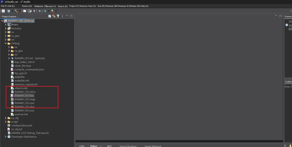
The elf file generated after e² studio compiles successfully is mainly used for debugging and symbol resolution, while hex or srec files are more suitable for programming tools. The RA6M4_LED project in the resource pack has already generated hex and srec files in the Debug directory, so they can be directly added and programmed by RFP.
If a project only generates an ELF file, you can enable the "Create Flash Image" option in the project properties, or use arm-none-eabi-objcopy to convert the ELF file to Intel HEX format. For evaluation documents, clearly explaining the differences between ELF, HEX and SREC will help readers better understand why the RFP requires selecting a HEX file.
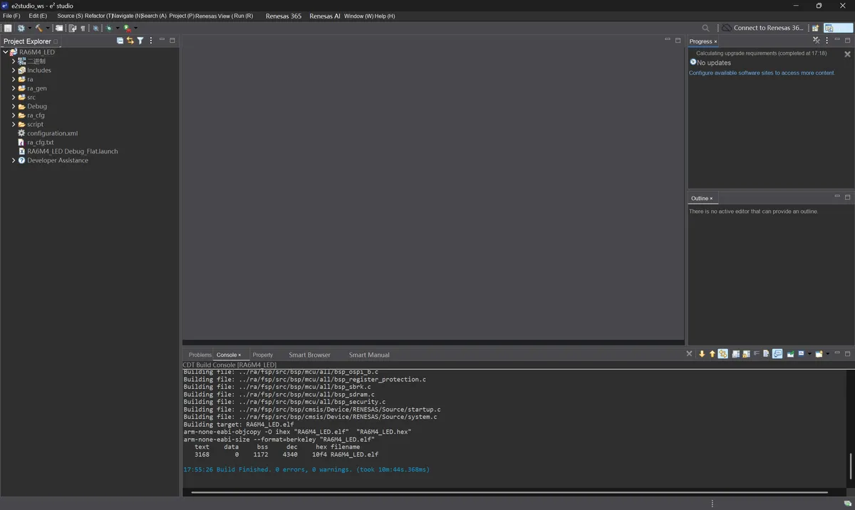
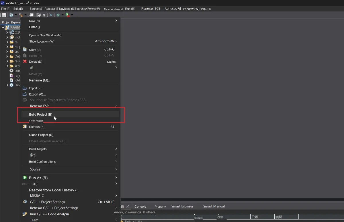
After selecting the RA6M4_LED project, execute Build Project. Once the build succeeds, the RA6M4_LED.elf, RA6M4_LED.hex, RA6M4_LED.srec and map files will be generated in the Debug directory. You can select either the hex or srec file for RFP programming.
4. Program Download and Basic Experiment Verification
4.1 Description of Download Methods
It is particularly necessary to distinguish between "programming" and "debugging" here. The CH340 + SCI Boot combination can perform program programming, which is suitable for basic experiments and final firmware flashing; the SWD debugger supports both programming and in-circuit debugging, making it ideal for troubleshooting during the development phase. The former is adopted in this evaluation because the development board itself is already equipped with a CH340 Type-C interface, which lowers the entry barrier for users.
From the perspective of usage experience, the key to the RFP download method lies in Boot mode switching. As long as the COM port is correct and the chip enters the Boot state, RFP can stably read the information of the target device and perform erasure, writing and verification operations.
The RA6M4 development board supports multiple program downloading methods. J-Link, Renesas E2 Lite, CMSIS-DAP, etc. are SWD debugging and downloading methods, which enable breakpoint and single-step debugging in the e² studio. This evaluation uses the onboard CH340 Type-C interface to complete program programming via the SCI Boot mode in cooperation with the Renesas Flash Programmer.
4.2 CH340 Type-C and SCI Boot Download Process
SCI Boot is a download method provided by the internal Boot ROM of the MCU. When the chip is powered on or reset, it will determine whether to boot from the user Flash or enter the Boot download state according to the boot mode pins. Therefore, before clicking RFP Connect, you need to switch the MODE / BOOT jumper and reset the chip to make it enter the correct state.
After the programming is completed, you must switch back to the Internal Flash mode; otherwise, the chip will remain in the Boot download process, and the user program will not run properly. This step is easily overlooked in experiments and is also a common cause of the LED not blinking.
- Connect the CH340 interface of the development board to a computer using a Type-C data cable.
- Confirm the COM port corresponding to CH340 in Device Manager.
- Switch the MODE/BOOT jumper on the development board to the SCI Boot mode.
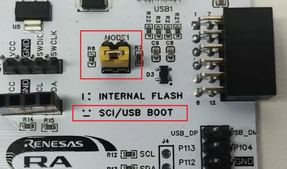
- Reset the development board or power it on again to put the chip into the Boot download state.
- Open Renesas Flash Programmer and select COM port in the Tool option.
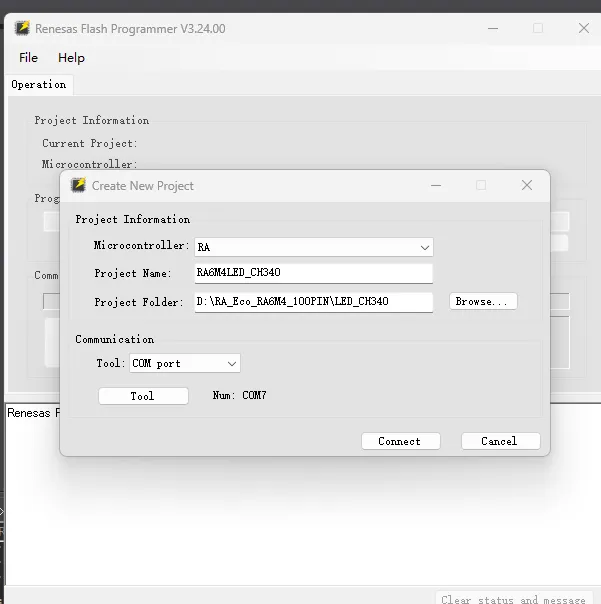
- Select the COM port corresponding to CH340 and connect to the target chip.
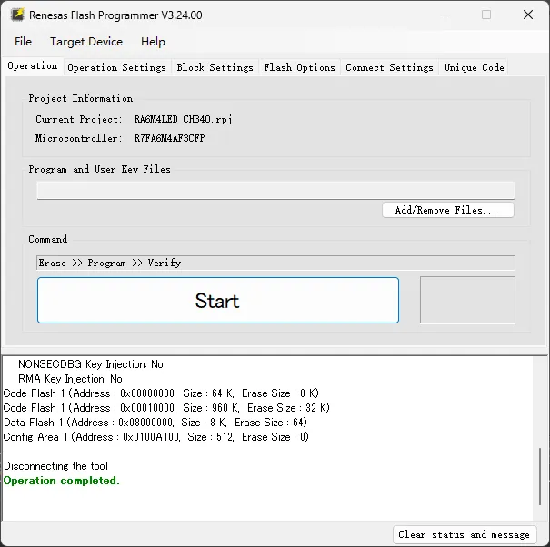
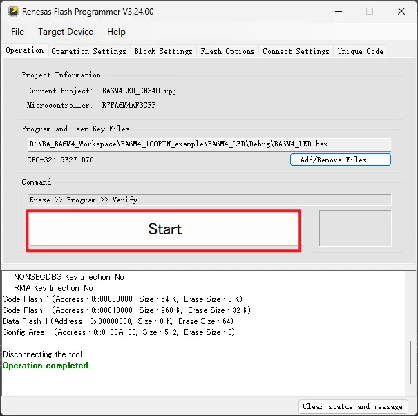
- Add the RA6M4_LED.hex file.
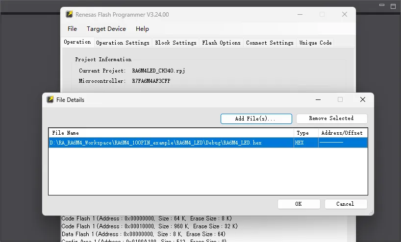
- Perform Erase, Program, and Verify operations.
- After the programming is completed, switch back to Internal Flash mode and reset to run.
4.3 Renesas Flash Programmer Connection Settings
When creating a new project in RFP, select RA for Microcontroller and COM port as the communication tool. Unlike some older versions of the tool, the current interface does not directly prompt users to manually select the complete device model in the creation window; instead, it reads the chip signature and displays the specific device information after a successful connection.
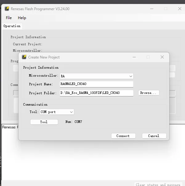
When the status window displays "Device: R7FA6M4AF3CFP", "Boot Firmware Version" and the Flash region information, it indicates that the computer, CH340, Boot mode and the target chip have successfully established communication. At this point, add the hex file and perform the flashing operation.
When creating a new project in RFP, select "RA" for Microcontroller, "COM port" for Tool, and the port corresponding to CH340 as the serial port number. After a successful connection, RFP will read the chip signature information and identify the target device as R7FA6M4AF3CFP.
4.4 Flash RA6M4_LED.hex
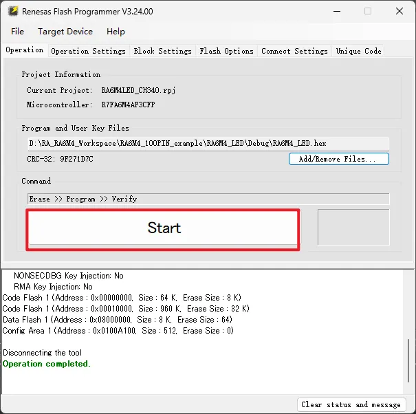
Selecting Erase, Program, and Verify as the programming commands can ensure a more reliable downloading process. Erase is used to wipe the target Flash area, Program writes the hex file into the chip, and Verify checks and validates the written content. For evaluation experiments, the verification step can enhance the credibility of the conclusions.
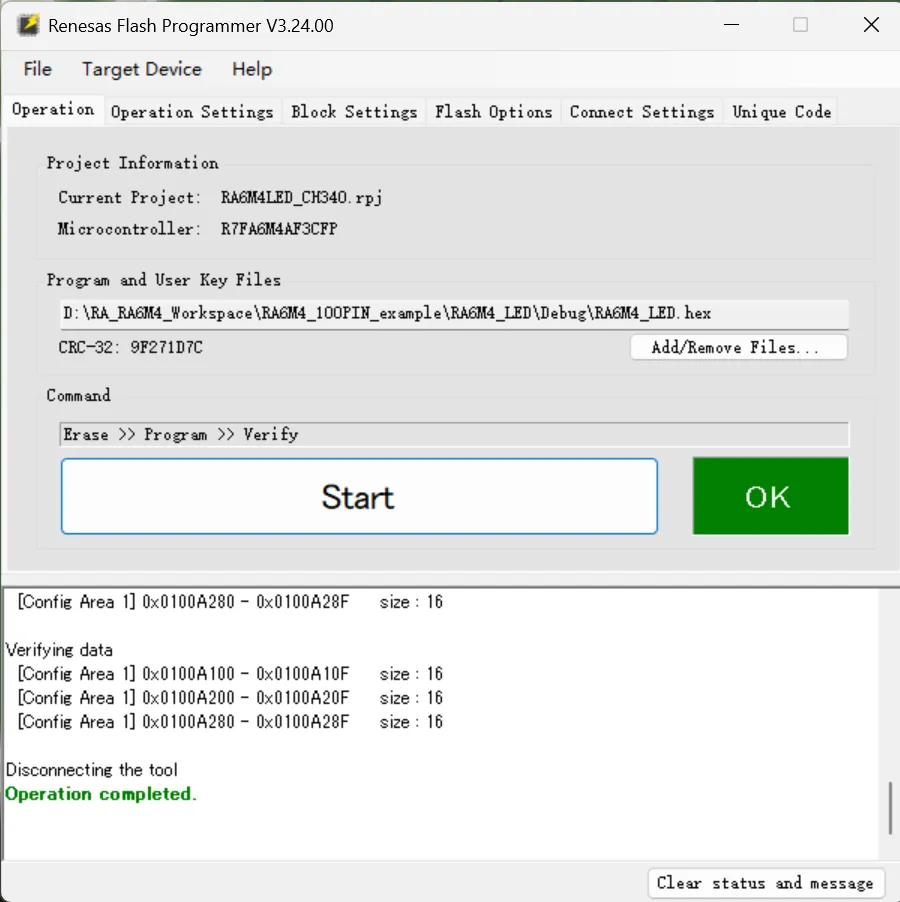
If the programming fails, you should first check the error code in the RFP status window. Issues related to file format, serial port occupation, Boot mode, power supply and target chip status usually come with relatively clear prompts in this window.
Add RA6M4_LED.hex to Program and User Key Files, select Erase, Program, and Verify as the commands. After clicking Start, RFP will sequentially erase the Flash, write the program and verify the data. Once the programming is completed, the status window will display "Operation completed".
4.5 Switch back to Internal Flash and reset for operation
The Internal Flash mode is the boot mode for normal operation of the user program. After the programming is completed, the LED sample program has been written to the internal Flash of the chip, but the CPU will only start running from the entry point of the user program after switching back to the normal boot mode and performing a reset.
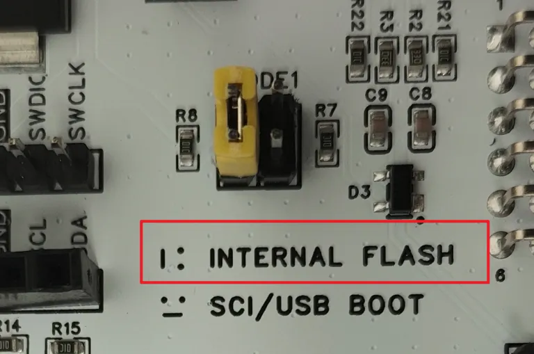
This step can be used as a fixed check item in the evaluation process: complete the programming, disconnect the connection, switch back to Internal Flash, perform a reset, and observe the phenomenon. Operating in this sequence can reduce misjudgments of "successful programming but the program does not run".
After the program burning is completed, switch the MODE/BOOT jumper back to the Internal Flash normal boot mode, then press the reset button or power on the device again. The chip will boot from the on-chip Flash and run the LED example program.
4.6 LED Blink Experimental Phenomenon
The significance of the LED Blink experiment lies in verifying the closure of the entire development chain. In the program, FSP initialization is performed first, then it enters the main loop of hal_entry, and the on/off state of the LED is controlled through the delay function and the IO write function. When the phenomenon is stable, it indicates that the basic clock, GPIO, downloading and booting processes are all functioning properly.
In terms of source code readability, the calling method of R_IOPORT_PinWrite is relatively intuitive, with parameters including the IOPORT control structure, the specific port pin, and the output level. If you need to change the blinking frequency, you only need to adjust the delay time of R_BSP_SoftwareDelay.
In the RA6M4_LED example project, the R_IOPORT_PinWrite function is used in hal_entry.c to control the three LED pins P210, P211, and P214, and a 500 ms delay is implemented via the R_BSP_SoftwareDelay function. After the program runs, the onboard LEDs turn on and off in a fixed cycle.
LED blinking.mp4 12.6 MB
4.7 Serial Port Printing Experiment Verification
Serial port printing is one of the most commonly used observation methods in embedded debugging. After using the RA6M4_PRINTF project, you can output running logs, variable values or sampling results through the COM port corresponding to CH340. Compared with only observing LEDs, serial port printing can provide richer operating status information.
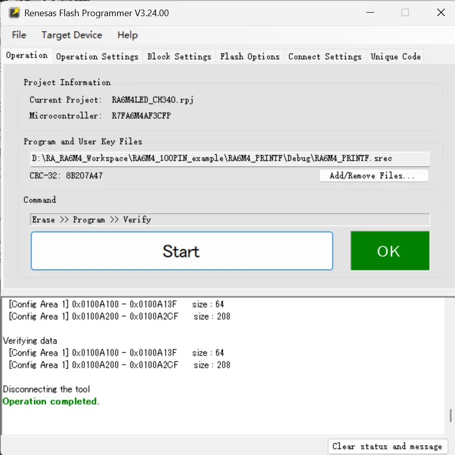
In the serial port experiment, it is necessary to confirm that the SCI channel configured by the program is consistent with the pins connected to the onboard CH340, and the baud rate of the serial port assistant must also be consistent with that configured by the program. If garbled characters appear, the baud rate, data bits, stop bits and clock configuration are usually checked first.
The TX LED indicator on the board is flashing:
Print receive.mp4 11.3 MB
In the serial port printing experiment, use the RA6M4_PRINTF or the serial port example project to observe the output data through the COM port corresponding to CH340. The parameters of the serial port tool are usually set to 115200 bps, 8 data bits, no parity, and 1 stop bit. The stable information output from the serial port indicates that the CH340 communication channel and SCI configuration are working properly.
The serial port assistant is now receiving messages:
20260811-1126-55.1414798.mp4 1.2 MB
4.8 Troubleshooting Download Failures
When a download fails, do not rush to modify the code. Instead, first determine whether the failure occurs in the connection phase, erase phase, write phase or runtime phase. Failures in the connection phase are mostly related to Boot mode, COM port, serial port occupation and cables; failures in the write or verification phase require checking the file, power supply and Flash status; for abnormalities in the runtime phase, focus on checking the boot mode and project configuration.
In this evaluation, the fact that RFP can read the chip signature serves as critical evidence for determining the availability of the download link. As long as the signature can be read stably, programming issues can usually be further located through file selection, boot mode and project configuration.
- Make sure that the development board has been switched to SCI Boot mode, and complete a reset or power cycle before connection.
- Confirm that in the RFP, select COM port for Tool, and the COM port shall be the corresponding port of CH340.
- Make sure that the serial port is not occupied by a serial port assistant, the e² studio Terminal, or any other software.
- Confirm that the programming file is RA6M4_LED.hex or RA6M4_LED.srec.
- After the programming is completed, confirm that MODE / BOOT has been switched back to Internal Flash.
- If using SWD for debugging, ensure that the debugger type matches the e² studio Debug Configuration.
5. Quick Start Lab
5.1 Sample Project Resources
Official Resource Links:
https://gitee.com/ramcu/ra-eco-ra6-m4-100-pin-v2.0The resource package comes with 14 sample projects, covering common getting-started paths ranging from basic GPIO to ADC/DAC, RTC, PWM, OLED, touch, UART and WS2812B. It is recommended to follow the evaluation sequence starting from LED/PRINTF/GPIOINPUT, and then proceed to experiments on ADC, PWM, RTC, touch and display categories.
Sample Project | Functional Direction | Recommended Evaluation Records |
RA6M4LED | LED Blinking / GPIO Output | compile results, download methods, and LED status photos |
RA6M4PRINTF / RA6M4USRT | Serial Port Printing and UART Communication | Serial port number, baud rate, terminal screenshot, stability |
RA6M4GPIOINPUT / RA6M4EXIT | Key Input and External Interrupts | Key response, debouncing performance, interrupt trigger log |
RA6M4ADC / RA6M4DAC / RA6M4DTCADC | Analog sampling, DAC output, DTC transfer | Sampled values, waveform screenshots, and CPU usage observation |
RA6M4GTPPWM | Timer PWM | Frequency, duty cycle, oscilloscope waveform |
RA6M4RTC / RA6M4TOUCH | RTC and Capacitive Touch | Timing accuracy, touch threshold and false touch performance |
RA6M4OLED / RA6M4WS2812B / RA6M4H3003 | Display, LED strip, and sensor expansion | Peripheral connections, display performance and interface compatibility |
5.2 ToF Ranging Application
Here, we use VL53L5CX , VL53L5CX is a STMicroelectronics multi-region ToF sensor, using FlightSense technology, can output 8x8 matrix ranging data, support multi-Object Detection, maximum frame rate 15Hz, ranging up to 4 meters, built-in field of view programmable function, integrated 940nm infrared laser emission and SPAD receiver array.
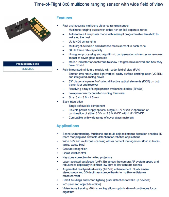
VL53L5CX is an 8×8 multi-zone FlightSense technology-based ToF sensor from STMicroelectronics, which adopts a 940nm laser and SPAD array, supports a maximum ranging distance of 4 meters and a frame rate of 60Hz, can realize multi-Object Detection and area motion judgment, features a 63° field of view, has a built-in histogram algorithm to suppress crosstalk, and is widely used in 3D scene perception, gesture recognition, robot obstacle avoidance and other scenarios.
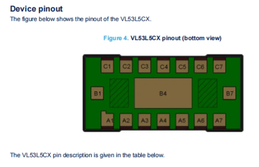
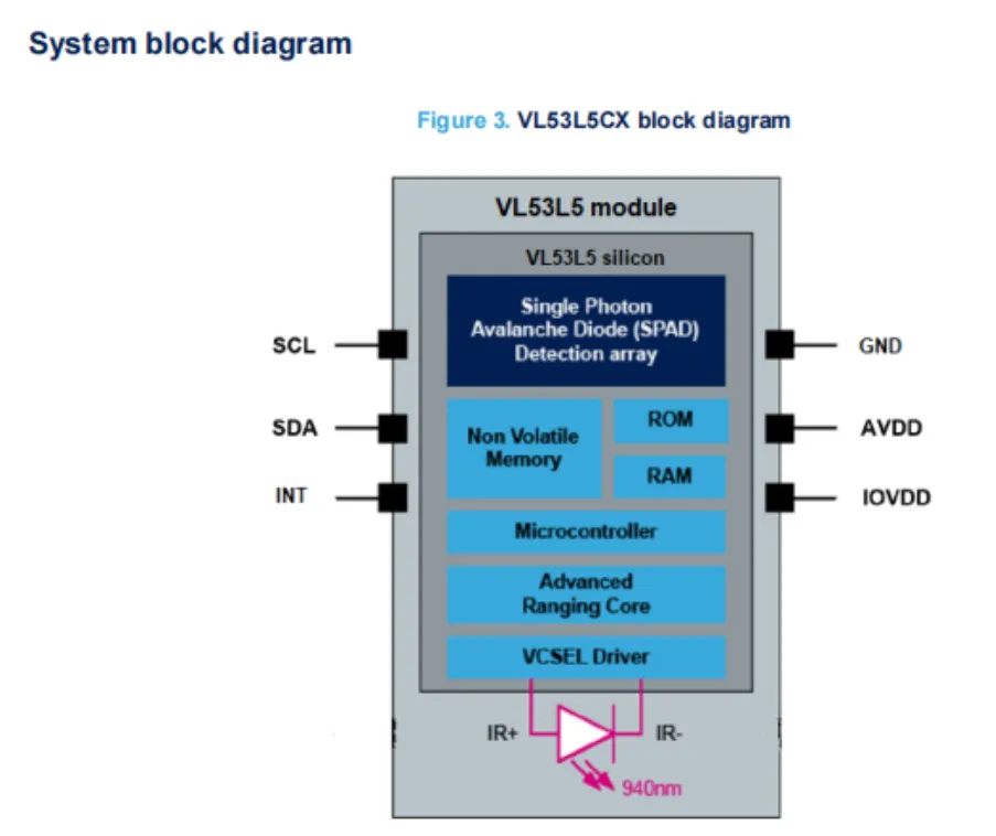
VL53L5CX operates based on the direct Time-of-Flight (ToF) principle: the VCSEL driver circuit emits 940nm infrared laser, the reflected light from the target is received by the Single Photon Avalanche Diode (SPAD) array, the ranging core and microcontroller calculate the round-trip time of light to convert into 8×8 multi-zone distance data, which is finally output via the I²C interface (SDA / SCL). The INT pin can output interrupt signals, and AVDD and IOVDD supply power for the analog / VCSEL and digital core respectively.
Here, after we finish downloading the corresponding driver package online, the running result is as follows:
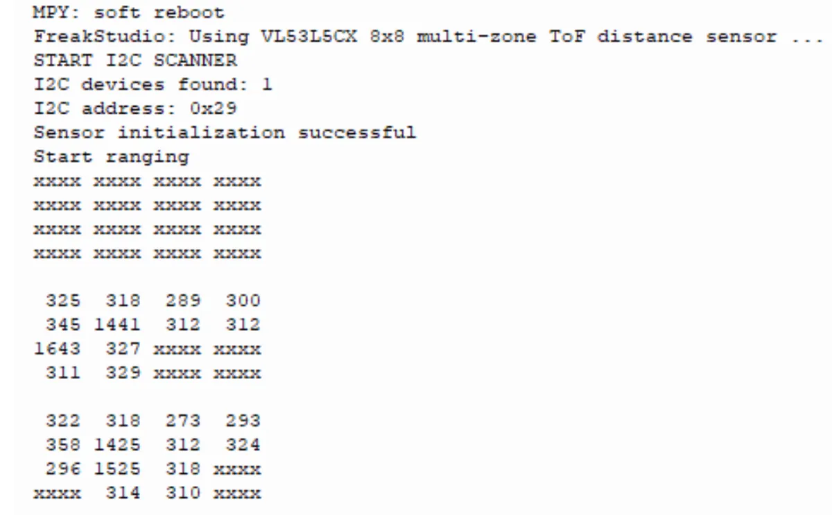
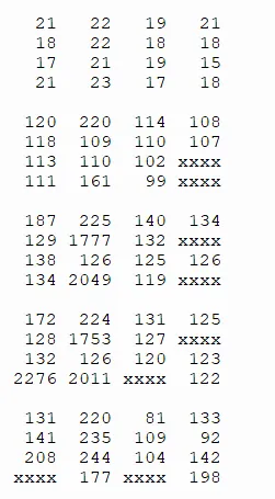
The VL53L5CX 8×8 multi-zone ToF sensor functions properly in terms of I2C communication and initialization; after ranging is initiated, it outputs 8×8 grid distance data that updates in real time as objects move closer or farther, with some invalid zones displaying xxxx, and the sensor exhibits normal multi-zone ranging response.
6. Evaluation Summary
6.1 Summary of hardware Resources
In terms of hardware, the RA-Eco-RA6M4-100PIN-V2.0 features balanced resource allocation. The board is equipped with LEDs, push buttons and serial ports suitable for entry-level verification, as well as PMOD interfaces, touch keys and external memory interfaces for extended experiments. Its 100-pin package allows the peripheral capabilities of the MCU to be fully demonstrated.
For learners, the onboard CH340 lowers the threshold for program downloading; for advanced developers, the SWD interface retains the complete debugging path. Therefore, this board is suitable not only for basic experiments but also for further verification of complex peripherals and applications.
The RA-Eco-RA6M4-100PIN-V2.0 development board is built around the R7FA6M4AF3CFP, with on-board resources covering basic input/output, serial port download, SWD debugging, PMOD expansion and common experimental peripherals. For learning the RA6M4 and verifying FSP peripheral drivers, its hardware resources are relatively complete.
6.2 Software Ecosystem and FSP Usage Experience
The advantage of FSP lies in that it encapsulates a large number of low-level initializations into graphical configuration and driver instances. For chips with a rich set of peripherals such as the RA6M4, starting configuration entirely from registers would incur a relatively high learning curve; with FSP, users can complete the initialization of clocks, pins and peripherals much faster.
Of course, FSP does not mean that there is no need to understand the underlying layer at all. During actual debugging, you still need to grasp concepts such as pin multiplexing, peripheral clocks, trigger sources and interrupt priorities. A more reasonable learning path is to first run the examples with FSP, and then gradually read the generated code and the hardware manual.
The combination of e² studio and FSP can deliver a complete development workflow covering chip selection, pin configuration, clock configuration, and peripheral driver instance generation. For MCUs with rich peripherals such as the RA6M4, the graphical configuration approach of FSP can significantly reduce the workload of low-level initialization.
6.3 Experience of CH340 Download Method
The biggest advantage of the CH340 + RFP download method is its low hardware threshold, as only a Type-C data cable is required to complete basic programming. This method is extremely practical in scenarios where no J-Link or E2 Lite is available.
Its limitations are also very clear: it can only perform programming and serial communication, and does not support in-circuit debugging. Therefore, in the evaluation conclusion, it should be positioned as an entry-level and basic verification solution, rather than a complete development and debugging solution.
The onboard CH340 Type-C interface, in conjunction with SCI Boot and Renesas Flash Programmer, enables program flashing, reducing reliance on external debuggers during the getting-started phase. In practical use, the key steps are to correctly switch the Boot mode, select the appropriate COM port, and switch back to Internal Flash boot after the flashing is completed.
6.4 Suggestions for SWD Debugging Extension
When the experiment progresses from LEDs and serial ports to USB, Ethernet, RTOS or TrustZone, it is recommended to connect an SWD debugger. Complex issues often cannot be located solely via serial port prints; breakpoints, call stacks, register and memory observation will significantly improve debugging efficiency.
If you use the RA6M4 for long-term project development, it is recommended to prepare one of J-Link, Renesas E2 Lite or CMSIS-DAP, and create the corresponding Debug Configuration in e² studio.
CH340 is suitable for programming and serial communication, but it does not support in-circuit debugging. When you need to perform breakpoint debugging, single-step execution, or view variables and registers, it is still recommended to use SWD debuggers such as J-Link, Renesas E2 Lite, or CMSIS-DAP.
6.5 Application Scenarios and Comprehensive Evaluation
From the overall usage experience, this development board has a clear positioning: it is not a minimal system board only for LED blinking, but a comprehensive experiment board suitable for systematic learning of RA6M4. It can cover multiple links including basic Development Environment, Boot download, GPIO, serial port, analog peripherals, timers, touch and external storage.
- Developers who want to learn the Renesas RA6/FSP project structure and get a quick hands-on experience with Cortex-M33 + TrustZone.
- Projects that require resources such as USBFS, CAN, I2C, SPI, UART, ADC, DAC, PWM, RTC, and touch for medium-complexity prototype verification.
- Engineering teams that expect to lead out as many pins of the 100PIN MCU as possible to facilitate wiring, measurement, reuse and secondary hardware design reference.
- It is necessary to compare selection evaluation scenarios for different MCUs in terms of their security capabilities, low-power capabilities, and peripheral combinations.
For article evaluation purposes, the highlights of this board can be summarized into three points: sufficient main control performance and resources, a wide coverage of example projects in the resource package, and the onboard CH340 which enables program flashing even without a debugger. The main area for improvement is that the instructions for download/boot mode need to be clear enough, otherwise first-time users are likely to confuse CH340 flashing with SWD debugging.
Overall, the RA-Eco-RA6M4-100PIN-V2.0 development board is suitable for getting started with RA6M4, conducting FSP peripheral experiments, verifying serial port Boot programming, developing industrial control prototypes, and building IoT nodes. It features a high-performance main control unit, rich peripheral resources, a resource package covering multiple sample projects, and an onboard CH340 chip that lowers the threshold for basic experiments.
References
RA-Eco-RA6M4V2.0_SCH_Schematic3_2026-06-01-2.pdf 628 KB
RA6M4 Datasheet.pdf 1.3 MB
RA-Eco-RA6M4V2.0_SCH_Schematic3_2026-06-01-2.pdf 628 KB
RA-Eco-RA6M4-100PIN-V1.0 Development Board Manual.docx 502 KB