Contents
- I. Module Introduction
- II. Introduction to Main Chips
- 2.1 Chip Overview
- 2.2 Pin Definition
- 2.3 Functional Block Diagram
- 2.4 Performance Parameters
- 2.5 Reference Circuit
- 2.6 Chip Configuration
- 2.7 Communication Interfaces and Related Protocols
- 2.8 PCB Routing Precautions
- III. Instructions for Circuit Engineering and Module Usage
- 3.1 Circuit Source Engineering
- 3.2 Module Usage Instructions
- 3.3 Application Experiment
- IV. Drivers
- 5. BOM & Recommended Alternative Parts
- VI. Revision History
- VII. Relevant Materials
- 7.1 Chip Datasheet
- 7.2 Unique Icons for PCB Silk Screen
I. Module Introduction
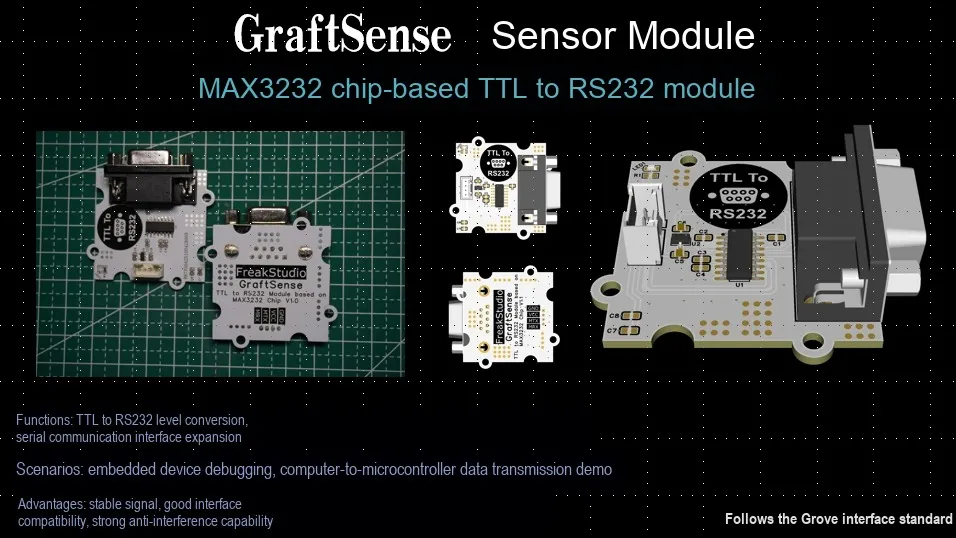
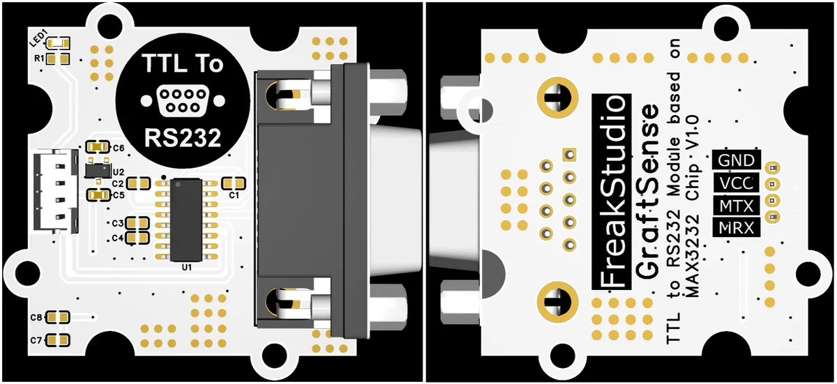
TTL to RS232 Module Based on MAX3232 Chip Adopting the MAX3232 chip, it enables bidirectional conversion between TTL level (0V to + 5V) and RS232 standard level (±3V to ±25V). Integrated with a DC-DC 5V-to-3.3V circuit, power filtering and power indicator, and using the D-DMR009PF-D002 terminal block as the RS232 interface, this module is applicable to scenarios such as industrial control and device serial port expansion, solving the communication compatibility problem of serial port devices with different levels, and providing a convenient conversion solution for communication between TTL level devices (e. g., microcontrollers) and RS232 level devices (e. g., industrial computers, legacy instruments).
II. Introduction to Main Chips
2.1 Chip Overview
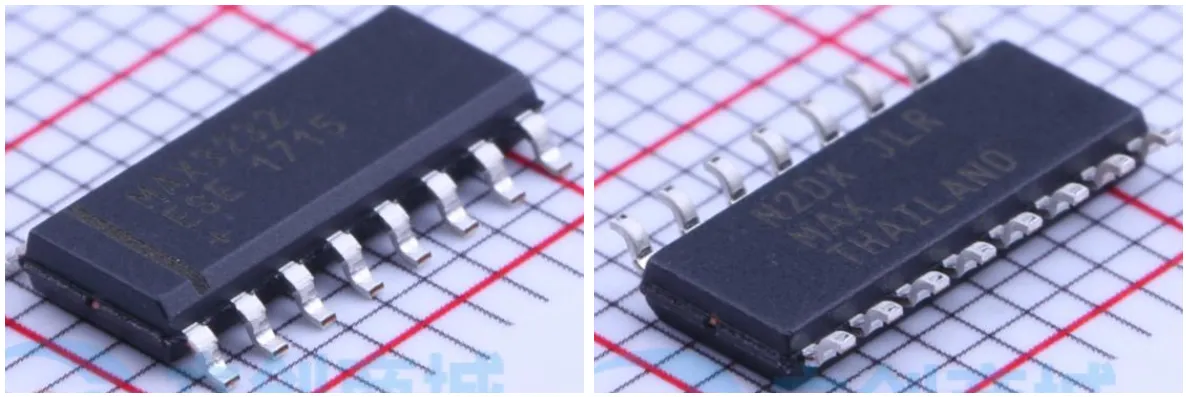
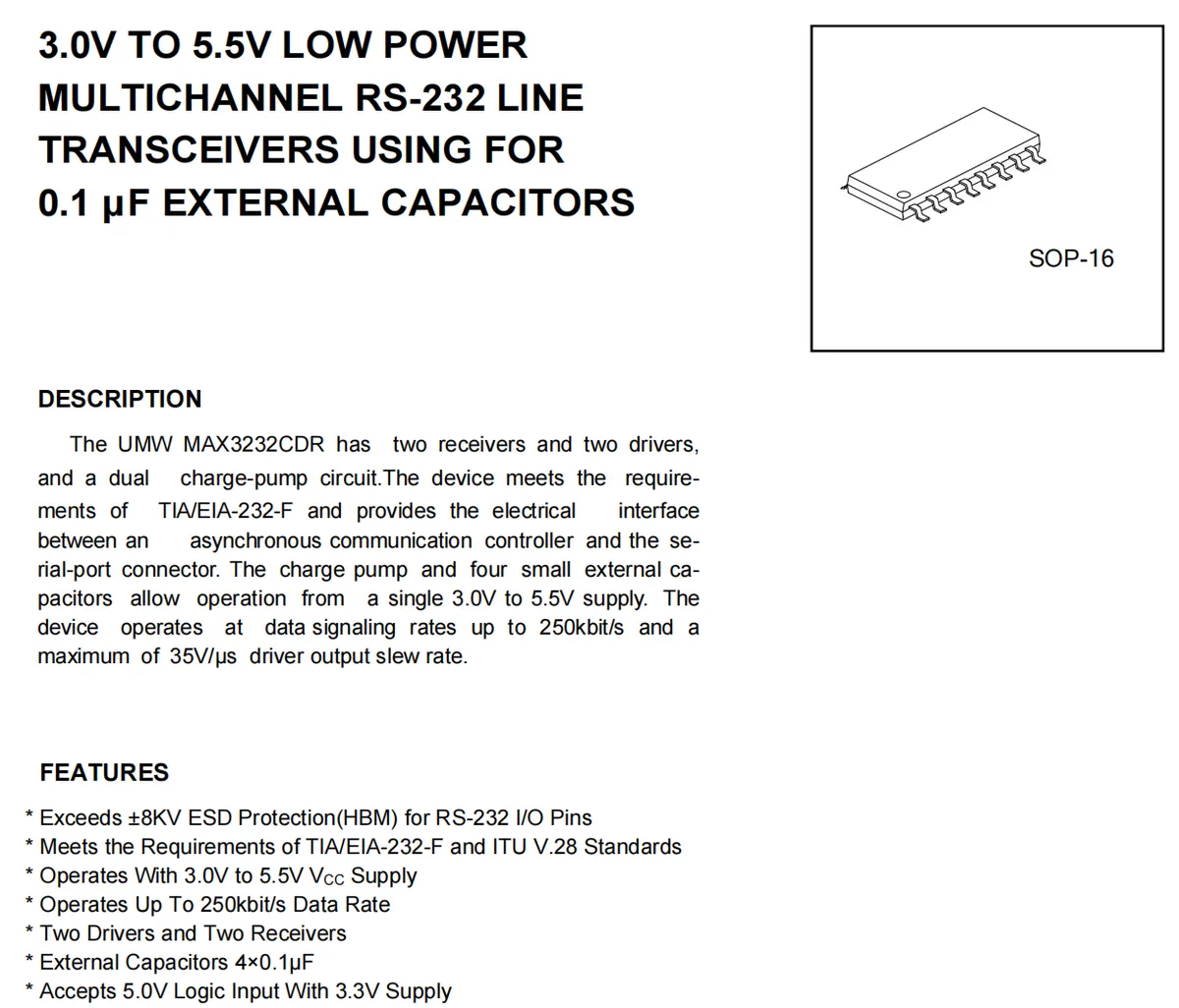
MAX3232 is a commonly used RS-232 to TTL (or CMOS) level converter chip. It supports a data transmission rate of up to 250kbps and dual-channel RS-232 to TTL (or CMOS) level conversion, and is widely used for serial communication between microcontrollers and devices such as computers, modems and printers.
2.2 Pin Definition
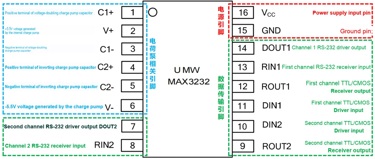
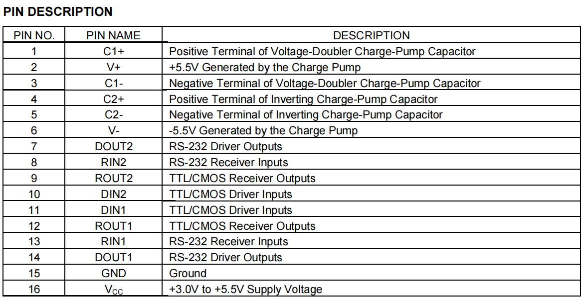
They are divided into the following three categories according to their functions:
- Charge Pump Related Pins: These pins are used for the operation of the internal charge pump, which generates the required voltages (+ 5.5V and -5.5V) via external capacitors to provide appropriate voltage levels for
RS-232drivers. - Power and Ground Pins: These
MAX3232pins supply power and ground to the chip to ensure its normal operation, with a supply voltage range of + 3.0V to + 5.5V. - Data transmission pins: used for
TTL/CMOSandRS-232level conversion, includingRS-232receiver input and output as well asTTL/CMOSdriver input and output.
2.3 Functional Block Diagram
Its working principle can be briefly summarized as follows: MAX3232 converts the input low voltage (e. g., 3.3V or 5V) into a high voltage that complies with the RS-232 standard (typically + 5V to + 15V and -5V to -15V) through its built-in charge pump circuit and inverters.
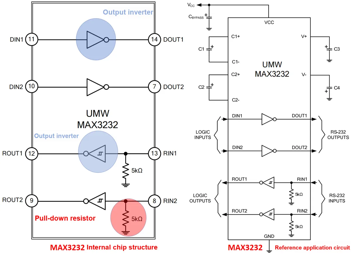
Here, the capacitance value required for the operation of the internal charge pump is related to the supply voltage:

RS-232 communication typically uses DB9 connectors;DB9 connectors have 9 pins, each of which serves a specific function in RS-232 communication. The pin numbers and corresponding functions are as follows:
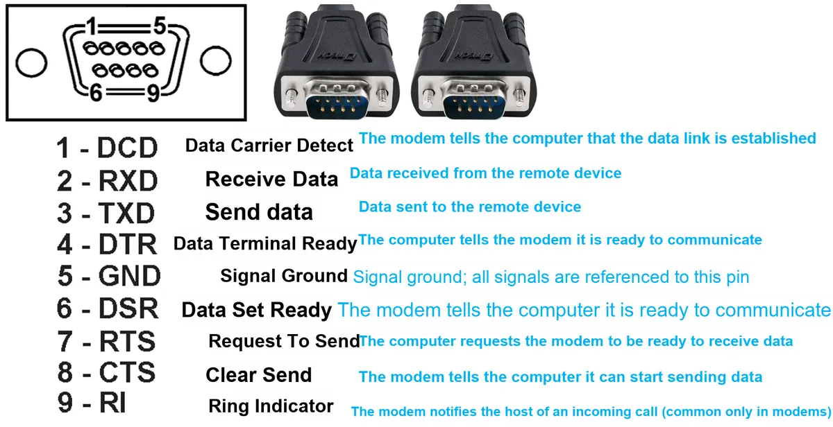
Here, we only use the DB9 connector's RXD, TXD and GND pins.
DB9 connectors come in two types: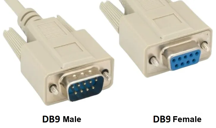
- Male connector (
Male): features 9 protruding metal pins - Female (
Female): features 9 small holes to receive the pins of the male connector
2.4 Performance Parameters
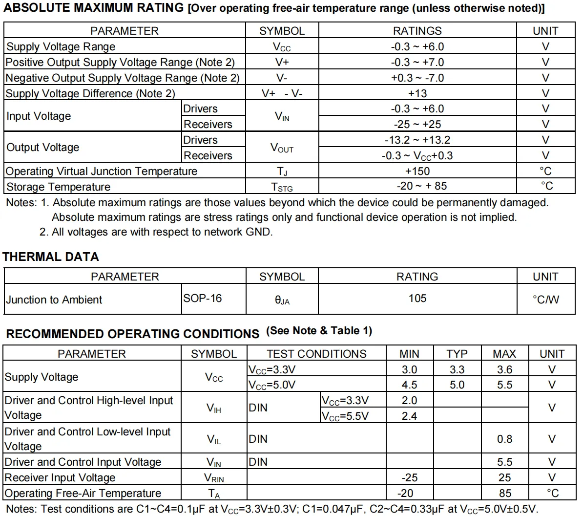
- Power Supply Voltage: The recommended operating voltages support 3.0-3.6V (typical 3.3V) and 4.5-5.5V (typical 5.0V), which shall be matched with the system power supply scheme.
- Operating Temperature: The recommended operating ambient temperature ranges from -20℃ to + 85℃, based on which the applicable scenario of the module (industrial grade / commercial grade) can be determined.
- Communication level: High level ≥ 2.0V (3.3V system), ≥ 2.4V (5.5V system); low level ≤ 0.8V, ensuring communication compatibility with
TTLlevel devices (such as microcontrollers). - Thermal Characteristics:
SOP-16The junction-to-ambient thermal resistance of the package is 105℃/W, and heat dissipation design shall be paid attention to in high-power scenarios.
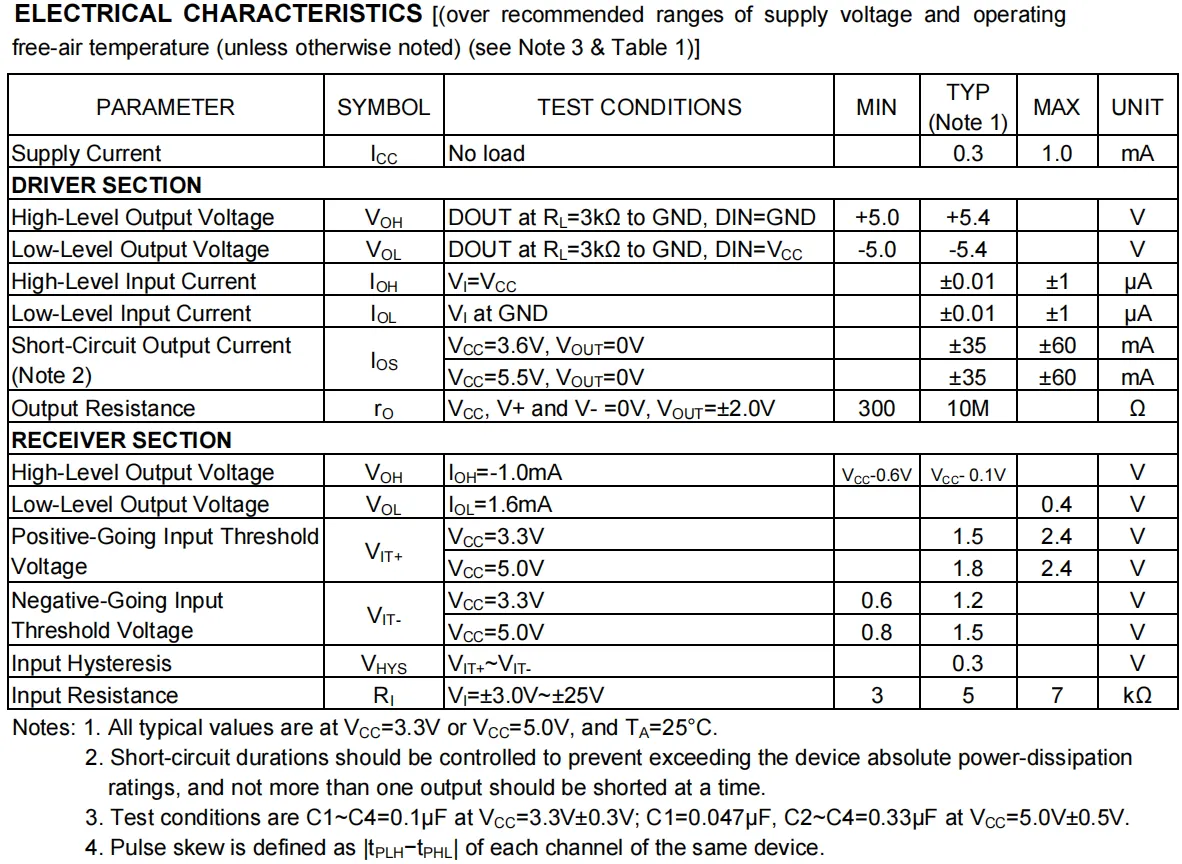
- Supply Current (
I₍CC₎): Typically 0.3mA at no load, maximum 1.0mA, which is relevant to module power consumption and power supply scheme design. - Driver high and low level output voltage (
V₍OH₎,V₍OL₎): Typical value is + 5.4V for high level and -5.4V for low level, which determines the signal driving capability and load adaptability. - Receiver high and low level output voltage (
V₍OH₎,V₍OL₎): For high level, when I₍OH₎=-1.0mA, the minimum value isV₍CC₎-0.6V, typical valueV₍CC₎-0.1V; for low level, whenI₍OL₎= 1.6mA, the maximum value is 0.4V, which affects the reliability of signal identification at the receiving end. - Input threshold voltage (
V₍IT+₎,V₍IT-₎): For example, whenV₍CC₎= 3.3V,V₍IT+₎has a typical value of 1.5V and a maximum value of 2.4V;V₍IT-₎has a typical value of 1.2V and a minimum value of 0.6V. It is the key to judging the high and low levels of input signals and ensures communication compatibility with external devices. - Input resistance (
R₍I₎): Typically 5kΩ, it affects the load-driving requirement of the signal source and is related to the selection and design of front-end equipment.
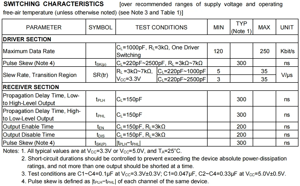
- Maximum data rate: Minimum 120 Kbit/s, maximum 250 Kbit/s, which determines the upper limit of the module's communication rate and is relevant to data transmission efficiency and system bandwidth design.
- Propagation delay time (
t₍PLH₎,t₍PHL₎): typically 300 ns, which affects signal transmission timing and is critical to the synchronization of high-speed communication. - Pulse
skew(t₍SK (p)₎): typically 300 ns, which reflects the timing deviation between channels and is related to the timing consistency of multi-channel communication. - Slew Rate (
SR (tr)): Typical value is 5 V/μs (varies under different loads), which determines the transition speed of signal edges and affects signal integrity and electromagnetic compatibility design.
2.5 Reference Circuit
None.
2.6 Chip Configuration
None.
2.7 Communication Interfaces and Related Protocols
None.
2.8 PCB Routing Precautions
None.
III. Instructions for Circuit Engineering and Module Usage
3.1 Circuit Source Engineering
To obtain the source code of the circuit, please follow the official account [Freak Embedded]
3.2 Module Usage Instructions
The schematic diagram of this module is shown below:
SCH_MAX3232-Based TTL to RS232 Module_v1.0_2025-11-22.pdf 2.0 MB
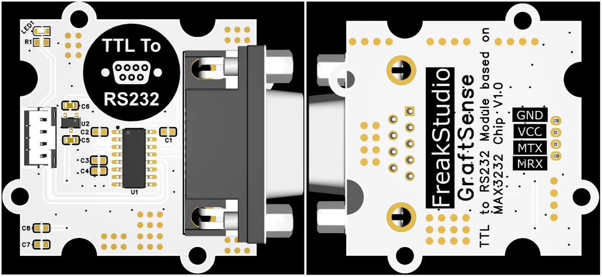
This module provides a UART interface: the MRX (corresponding to the UART MCU serial port RXD) of this module is actually connected to the TXD pin of the module, and the MTX (corresponding to the UART MCU serial port TX) is actually connected to the RXD pin of the module. Note that cross connection is strictly prohibited.
Next, use the USB to DB9 adapter to connect to the DB9 connector on the module.
Typically, the serial port of a computer or device uses a DB9 female connector, while one end of a serial cable is a DB9 male connector; the DB9 connector used on our module is a female type. On modern computers, DB9 connectors have long been phased out, but virtual serial ports (implemented via USB to serial conversion) are still functional. We can use a USB to DB9 adapter to enable communication between a microcontroller and a computer via the RS232 protocol.
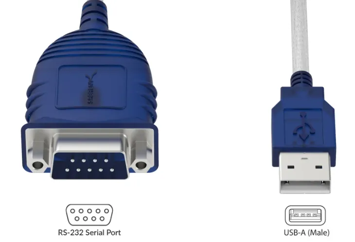
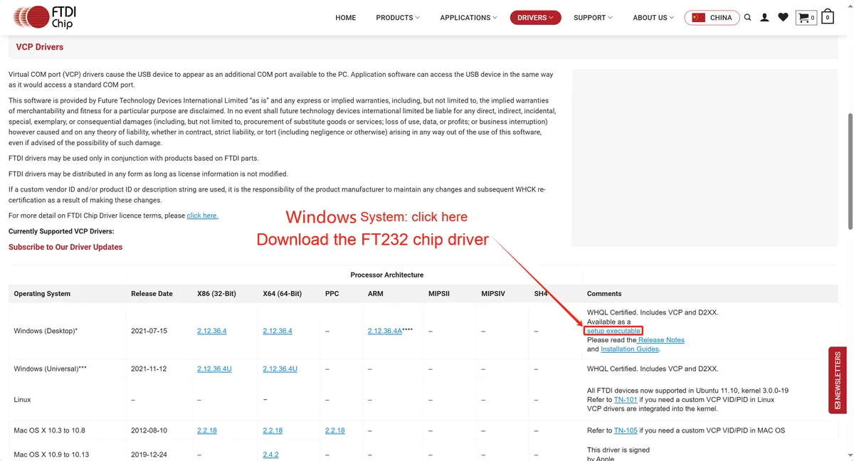
Here USB to RS232 adapters often use built-in FT232 chips to complete the conversion of different Communication Protocols, FT232 is a USB to serial chip designed by FTDI , which is widely used in embedded systems, microcontroller development and debugging, as well as the traditional RS-232 or TTL serial interface to USB interface, allowing modern devices to communicate with old serial devices.
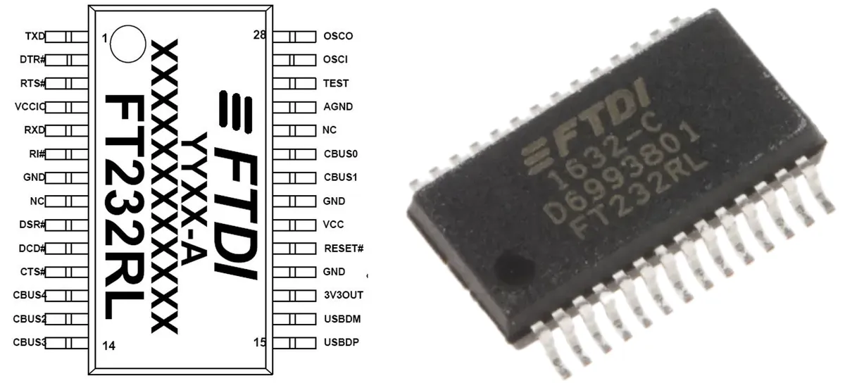
The FT232 chip requires the driver provided by FTDI to be installed in most operating systems, which can be downloaded from FTDI's official website:
https://ftdichip.com/drivers/vcp-drivers/
-to- USB -to- RS232 adapter we provide adopts the domestic MS3020 chip, and its corresponding driver also needs to be installed. If you directly connect the USB -to- RS232 adapter to a computer without installing the matching driver, normal communication will not be available. The following content will be displayed when you open the Device Manager:
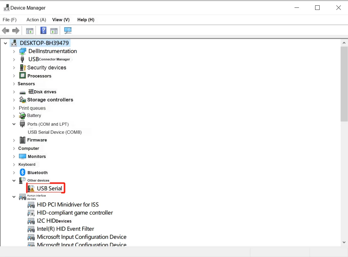
The driver download link is as follows: http://www.dtech.cn/download/download.php? class3= 410
Open the PDF file of the driver installation instructions and follow the steps to complete the installation:

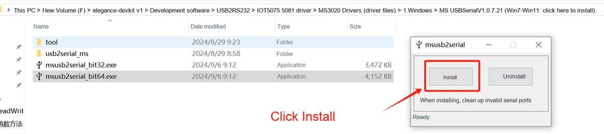
After the installation is successful, click on Device Manager again, and you will find that the small exclamation mark on the original device has disappeared, indicating that the device can be used normally. In the corresponding serial port communication software assistant, you can also select its port normally:
3.3 Application Experiment
Here, we use the GraftPort-RP2040 development board for testing, and connect the TTL-to-RS232 module based on the MAX3232 chip to communicate with the main controller via the UART interface.
Here, we first use the HY2.0-4P cable to connect the module to the GraftPort-RP2040 development board's UART1 interface, and meanwhile use the USB to RS232 adapter to connect to the module's DB9 interface:
The module connections are shown in the following table:
Development Board Pins | Module Pins | Description |
Pin 8 |
|
|
Pin 9 |
|
|
- |
| Connect to a computer for reading |
Serial Port Debugging Software XCOM, XCOM parameter configuration is as follows:
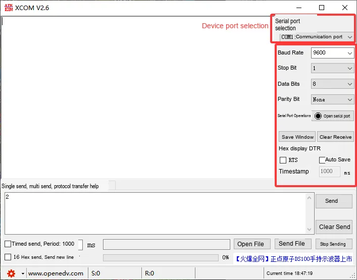
Copy the following test code for verifying the function of the validation module main.py into our project:
# Python env   : MicroPython v1.23.0
# -*- coding: utf-8 -*-
# @Time    : 2025/09/04 10:00
# @Author  : 侯钧瀚
# @File    : main.py
# @Description : 232 serial port loopback test code

# ======================================== Import Modules =========================================

from machine import UART, Pin
import time

# ======================================== Global Variables ============================================

# Test message counter
count = 1

# ======================================== Functions ============================================

# ======================================== Custom Classes ============================================

# ======================================== Initialization ==========================================

# Power-on delay of 3 s
time.sleep(3)
print("FreakStudio: UART loopback test started. Sending data every 2 seconds...")

# Initialize UART1: TX=Pin8, RX=Pin9, baud rate 9600
uart = UART(1, baudrate=9600, tx=Pin(8), rx=Pin(9))

# ========================================  Main Program  ===========================================

try:
    while True:
        # Build test message with counter
        test_msg = f"Test message {count}: Hello, UART loopback!"
        print(f"\nSent: {test_msg}")

        # Send message
        uart.write(test_msg.encode('utf-8'))

        # Wait a short time to receive data
        time.sleep(0.1)

        # Read and print received data
        if uart.any():
            received = uart.read(uart.any()).decode('utf-8')
            print(f"Received: {received}")
        else:
            print("Received: No data (check connections)")

        # Increment counter and wait 2 seconds before the next send
        count += 1
        time.sleep(2)
except KeyboardInterrupt:
    print("\nTest stopped by user")
To flash the code, open a terminal and use the mpremote tool to connect to the main controller; the output is as follows:
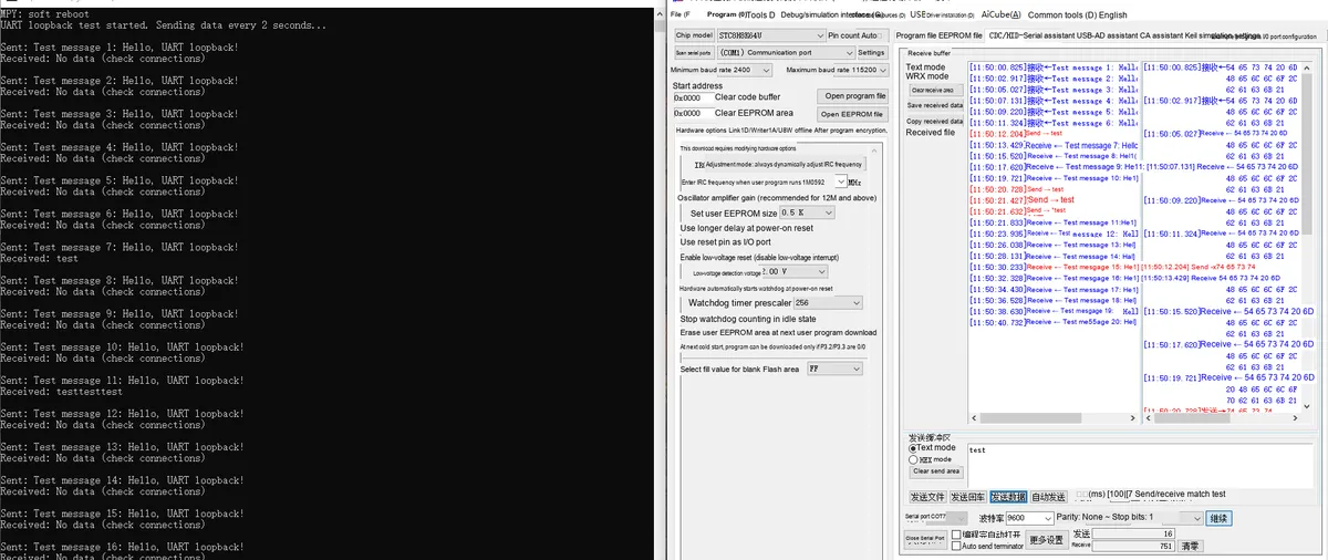
It can be seen that our module can normally complete the loopback test function of the serial port.
IV. Drivers
ttl_232_code.zip 1 KB
5. BOM & Recommended Alternative Parts
None.
VI. Revision History
Document Version | Date of Revision | Modifier | Revised Content |
v1.0 | 2025-11-22 | Li Zisheng | Initialize the document The BOM sheet has not been finally checked, the driver has not been re-verified, and the 3.3 application experiment Not yet specified. |
v1.1 | 2025-12-29 | Li Zisheng | Added application experiments and production files |
v1.2 | 2025-12-31 | Xin Ruili | Create an open version of the document based on the internal document version v1.1. |
VII. Relevant Materials
7.1 Chip Datasheet
C141882_D-SUB-VGA Connector_D-DMR009PF-D002_Datasheet_WJ227792.PDF 563 KB
C22449673_RS232 Chip_MAX3232IPWR(UMW)_Datasheet_UMW+MAX3232IPWR.PDF 498 KB
7.2 Unique Icons for PCB Silk Screen