Contents
- I. Module Introduction
- II. Introduction to Main Chips
- 2.1 Chip Overview
- 2.2 Pin Definition
- 2.3 Functional Block Diagram
- 2.4 Performance Parameters
- 2.5 Reference Circuit
- 2.6 Chip Configuration
- 2.7 Communication Interfaces and Related Protocols
- 2.8 PCB Routing Precautions
- III. Instructions for Circuit Engineering and Module Usage
- 3.1 Circuit Source Engineering
- 3.2 Module Usage Instructions
- 3.3 Application Experiment
- IV. Drivers
- 5. BOM & Recommended Alternative Parts
- VI. Revision History
- VII. Relevant Materials
- 7.1 Chip Datasheet
- 7.2 Unique Icons for PCB Silk Screen
I. Module Introduction
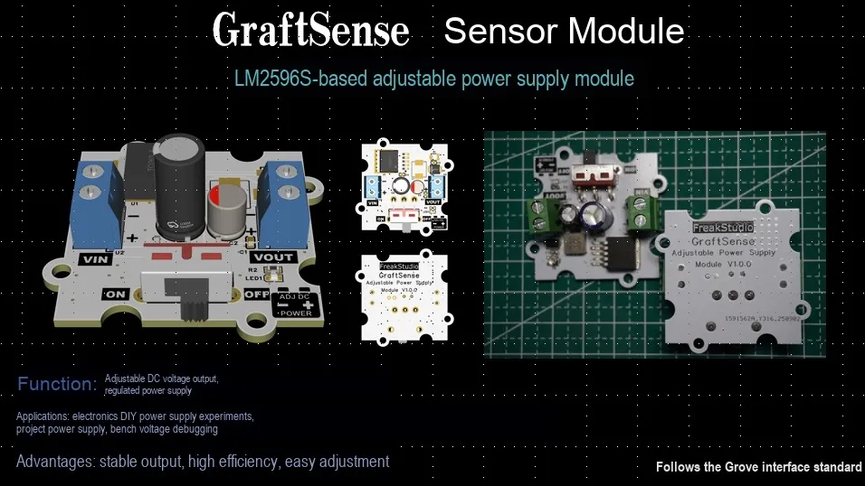
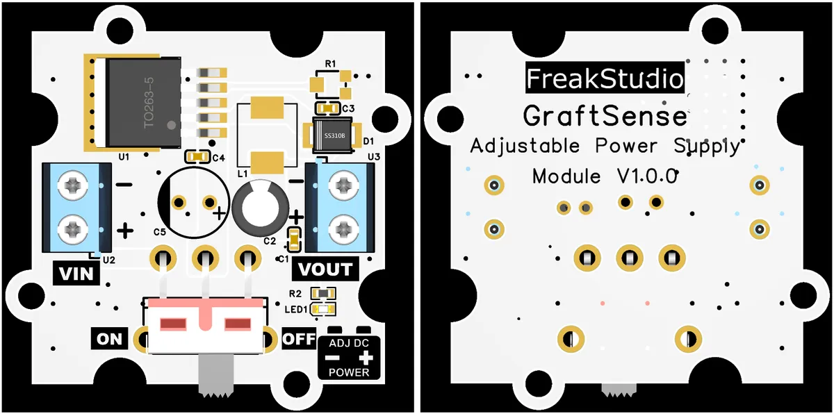
The adjustable power supply module based on LM2596S is a power conversion module designed based on the LM2596S-ADJ step-down DC-DC switching voltage regulator chip. It is used to stably convert a higher DC voltage into the required low-voltage output. Featuring a wide input voltage range and adjustable output characteristics, it integrates a power switch, status indicator light and complete filtering and protection circuit, can flexibly adjust the output voltage, and provides a stable and adjustable DC power supply for electronic devices. It is suitable for scenarios such as prototype development and equipment power supply.
II. Introduction to Main Chips
2.1 Chip Overview
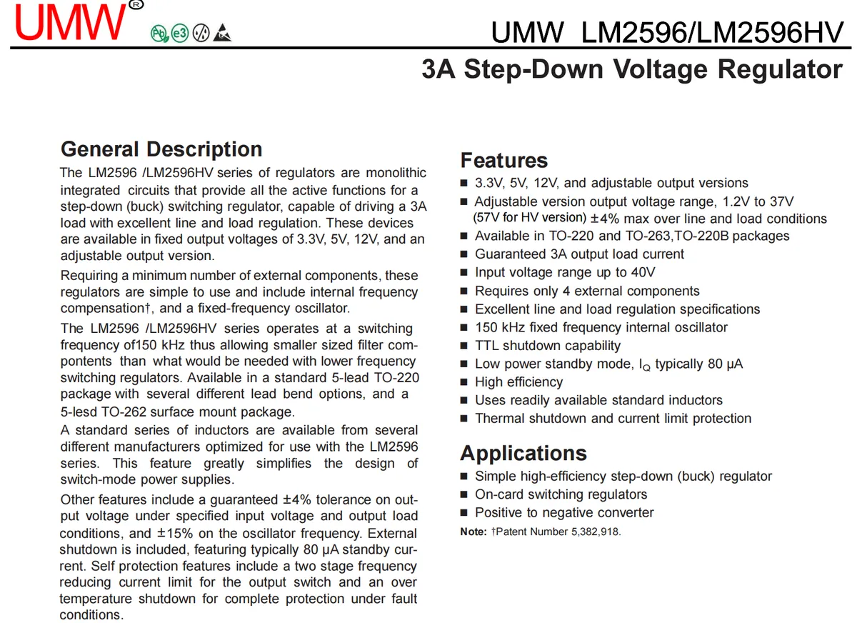
LM2596S-ADJ is a UMW LM2596 series adjustable-output step-down switching regulator. As a monolithic integrated circuit that integrates all active functions of a step-down switching regulator, it can drive a 3A load, features an output voltage range of 1.2V to 37V and a switching frequency of 150kHz, and only requires a small number of external components to achieve high-efficiency step-down voltage regulation. It is equipped with internal frequency compensation, a fixed-frequency oscillator, TTL shutdown capability and a low-power standby mode (with a typical standby current of 80μA), and also integrates thermal shutdown and current limiting protection functions. Suitable for scenarios such as high-efficiency step-down regulators and on-board switching regulators, it is a power management chip that delivers both high cost-performance and high reliability.
2.2 Pin Definition
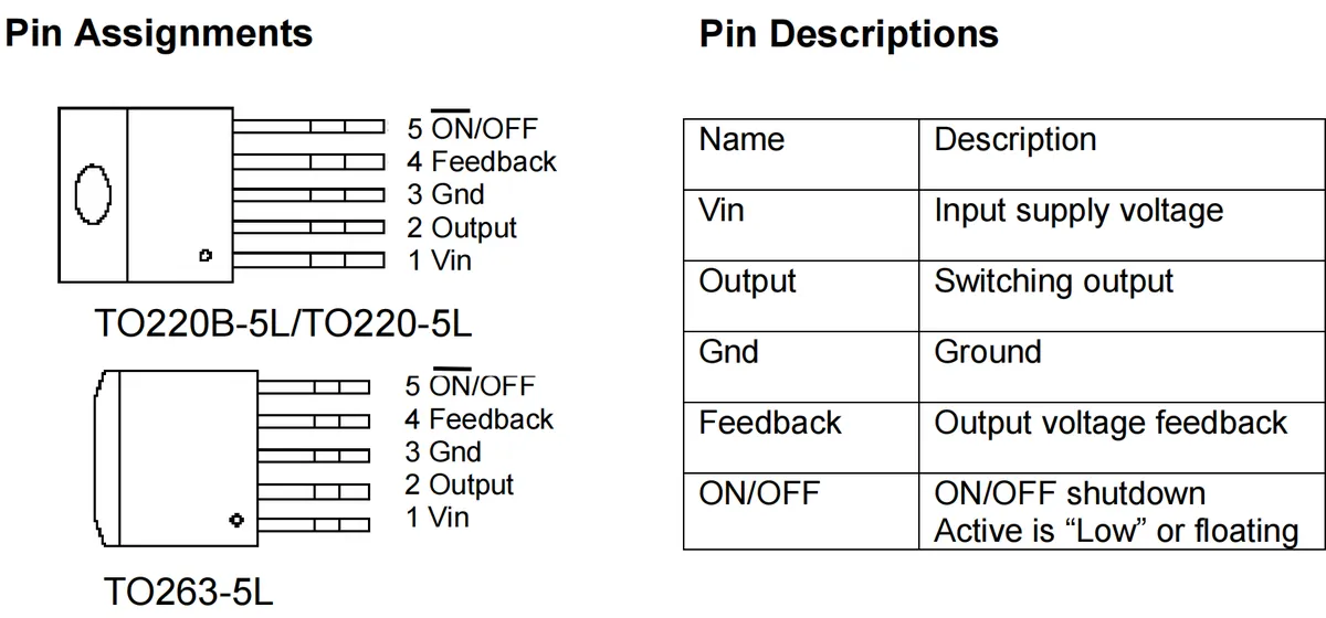
LM2596S-ADJ The functions of each pin of the chip are as follows:
Vin(Pin 1): Input power supply voltage terminal, connected to an external DC power supply, supporting a wide input range of 4.5V to 40V.Output(Pin 2): Switch output terminal, an internal switching node; an external energy storage inductor and freewheeling diode are required to implement step-down energy conversion.Gnd(Pin 3): Ground terminal, which provides a reference ground for the chip; a single-point grounding strategy shall be adopted to reduce EMI interference.Feedback(Pin 4): Output voltage feedback terminal, which collects voltage through an external resistor voltage divider network to achieve adjustable voltage regulation within the range of 1.2V to 37V.ON/OFF(Pin 5): Enable shutdown terminal. The chip operates when at low level (or floating), and shuts down when at high level, with the quiescent current dropping to approximately 80μA. It supportsTTLlevel start-stop control.
2.3 Functional Block Diagram
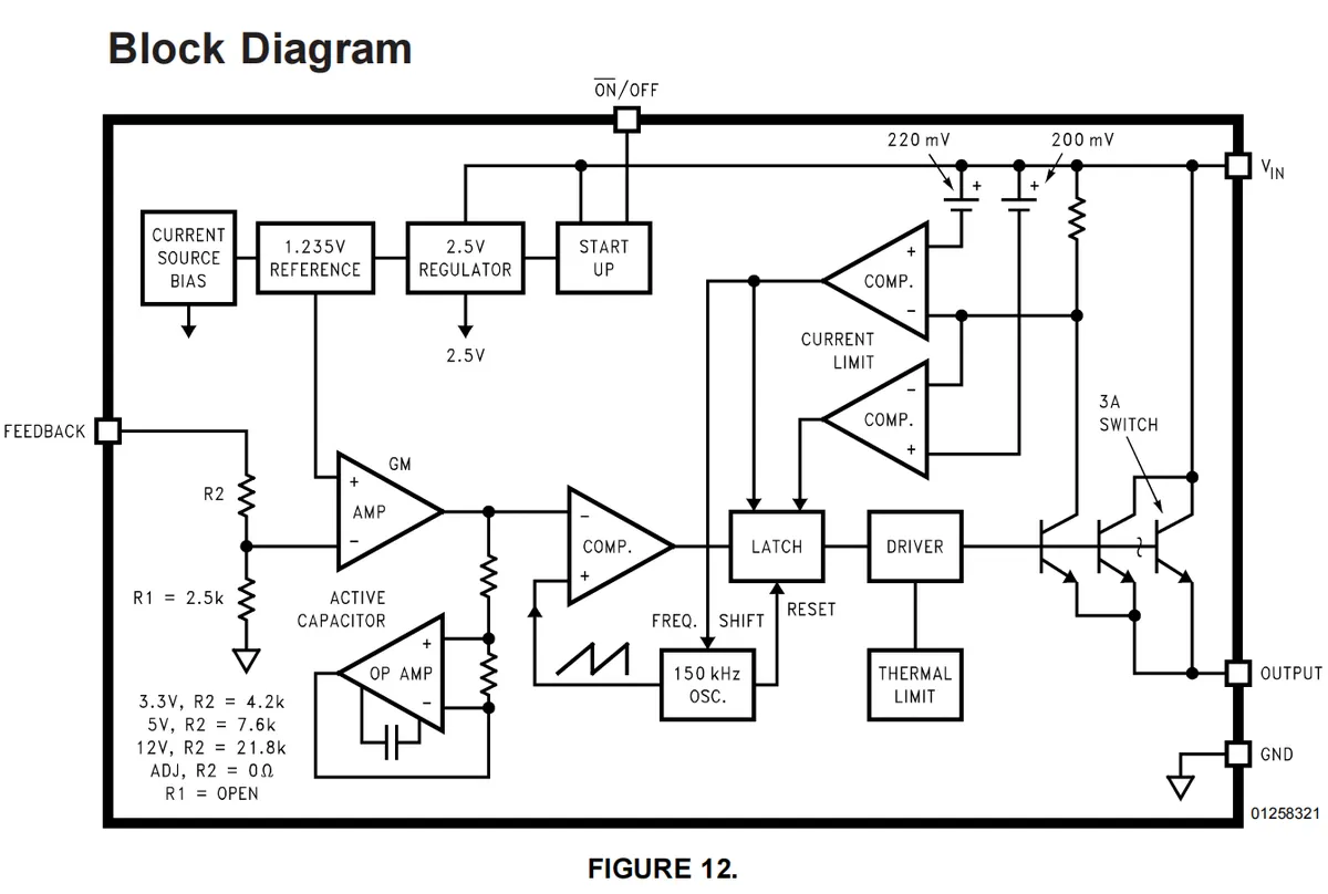
LM2596S-ADJ can be internally structured into five major modules: reference and bias, feedback and amplification, oscillation and control, switching and driving, and protection mechanism, with the functions of each part as follows:
- Reference and Bias Module
- Current Source Bias (
CURRENT SOURCE BIAS): It provides a stable bias current for all internal circuits to ensure that each module operates within a reasonable current range. - 1.235V Reference Source (
1.235V REFERENCE): Generates a precise 1.235V reference voltage, serving as the core reference for output voltage regulation (the output voltage formulaVOUT= 1.23V×(1+R2R1)is derived on this basis). - 2.5V Regulator (
2.5V REGULATOR): Generates a 2.5V internal regulated power supply to power modules such as comparators and amplifiers, ensuring their operational accuracy. - Start-up Circuit (
START UP): Triggers initialization when the chip is powered on, enabling the circuit to switch from standby to normal operating mode.
- Current Source Bias (
- Feedback and Amplification Module
- Transconductance amplifier (
GM AMP): Converts the voltage error at the feedback terminal into a current signal to participate in error amplification of the loop, serving as the core amplification stage for feedback regulation. - Operational Amplifier (
OP AMP) + Active Capacitor (ACTIVE CAPACITOR): constitutes a frequency compensation network that adjusts the frequency characteristics of the feedback loop, suppresses oscillation, and ensures the stability of the output voltage. - Error Comparator (
COMP): Compares the feedback voltage with the 1.235V reference, outputs an error signal to drive the subsequent control logic.
- Transconductance amplifier (
- Oscillation and Control Module
- 150kHz Oscillator (150 kHz
OSC): Generates a fixed-frequency clock signal that determines the switching frequency of the switching transistor, enabling the step-down conversion to operate at 150kHz, and supports compact design with small-sized inductors and capacitors. - Latch (
LATCH) + Frequency Shift (FREQ. SHIFT): It latches and transmits the control signal, and protects the chip through "frequency reduction and current limiting" in case of overcurrent; the frequency shift module adjusts the switching frequency in abnormal conditions to balance performance and protection.
- 150kHz Oscillator (150 kHz
- Switch and Drive Module
- Drive Circuit (
DRIVER): amplifies the control signal to drive the 3A Switch (3A SWITCH) to perform high-speed switching operations, thereby achieving step-down energy conversion from "input voltage to output voltage".
- Drive Circuit (
- Protection Mechanism Module
- Thermal Limit (
THERMAL LIMIT): Monitors the junction temperature of the chip, and triggers a shutdown when the temperature exceeds 150°C to prevent damage caused by overheating. - Current Limit Comparator (
CURRENT LIMIT COMP): It monitors the current of the switching tube, and limits the current when the current exceeds the threshold to realize overcurrent protection. ON/OFFControl Module: Receives an external logic level signal. The chip operates when the input is at a low level or floating, and enters shutdown mode (with quiescent current reduced to 80μA) when the input is at a high level, thereby achieving power consumption control.
- Thermal Limit (
These modules work in concert to endow LM2596S-ADJ with the features of high-efficiency step-down, wide-range adjustability and multiple protections, making it a classic choice for medium and small power supply designs.
2.4 Performance Parameters
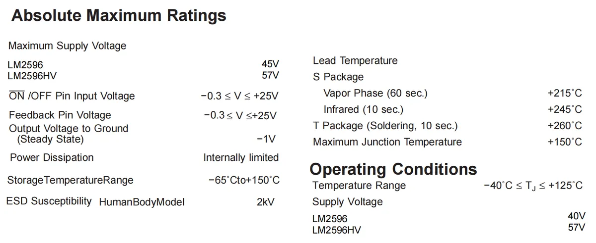
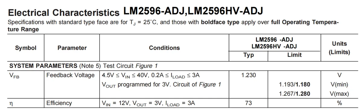
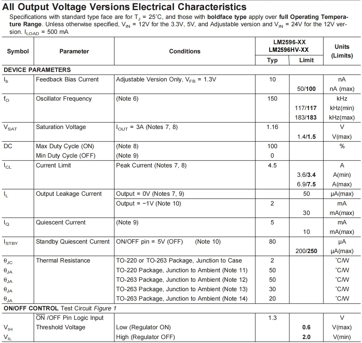
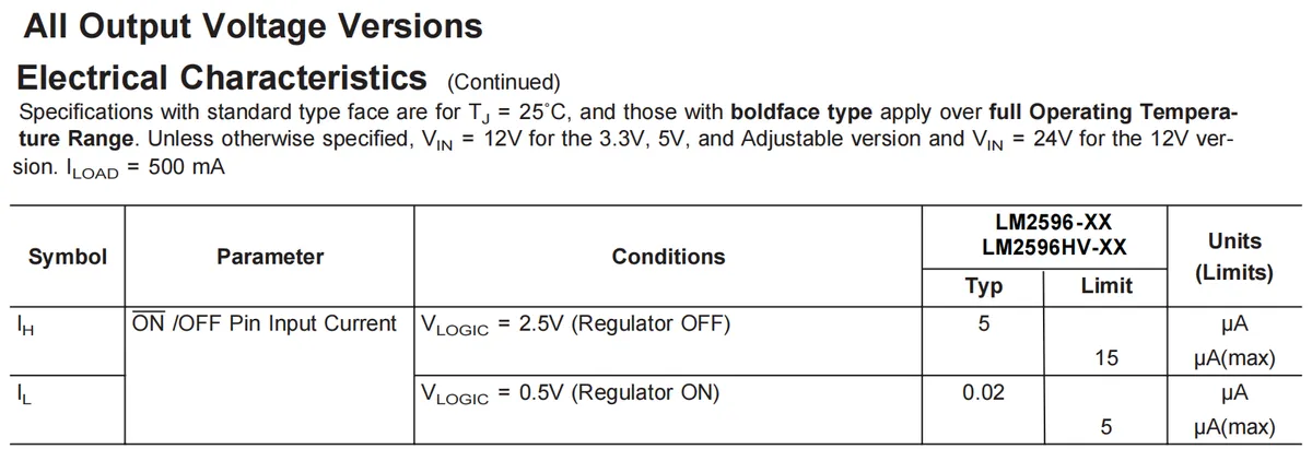
In the design and application of circuit boards, LM2596S-ADJ has the following core performance parameters that require key attention:
- Power Supply and Voltage Regulation: Input Voltage
LM2596≤40V, high-voltage version ≤57V; the feedback reference voltage of 1.23V is the core of output voltage regulation (output formulaVOUT= 1.23V×(1+ R2/R1)). The feedback resistors shall be placed close to the chip and away from the inductor to prevent magnetic flux from interfering with regulation accuracy. - Current and Protection: Maximum output current: 3A, typical efficiency: 73%(12V to 3V, 3A load); operating junction temperature: -40℃ to + 125℃, thermal shutdown activated when junction temperature exceeds 150℃;
ON/OFFpin enabled at low level (≤1.3V) and shut down at high level (≥2.0V); meanwhile, attention shall be paid toESDprotection (2kV for human body model) and soldering temperature (e. g. ≤260℃/10s for T package).
2.5 Reference Circuit
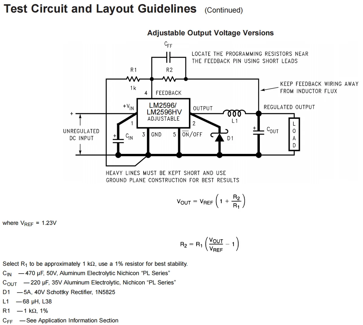
This is LM2596S-ADJ a reference circuit for the adjustable output version, which can be interpreted from three aspects: circuit structure, component functions, and layout key points.
- Circuit Structure and Component Functions
- Input Filtering:
CIN(470μF/50V aluminum electrolytic capacitor) is used to filter out input voltage ripple and provide a stable DC input for the chip. - Core Step-Down Component:
The LM2596S-ADJchip serves as the core, which achieves step-down voltage regulation through high-frequency switching of its internal power switch; Pin 2 (Output) is the switching node. - Energy storage and freewheeling:
L1(68μH inductor) stores energy and participates in voltage conversion,D1(1N5825 Schottky diode) provides a freewheeling loop when the switching transistor is turned off,COUT(220μF/35V aluminum electrolytic capacitor) filters output ripple to obtain a stable DC voltage. - Feedback Voltage Regulation:
R1(a 1kΩ, 1% precision resistor) andR2(a programmable resistor) form a voltage divider network, which enables adjustable output voltage via the formulaVOUT= 1.23V×(1+ R2/R1);CFFis a feedback compensation capacitor used to stabilize the feedback loop and prevent oscillation.
- Input Filtering:
- Key Points of Layout and Design
- High-current trace: The high-current paths marked by thick lines in the diagram (such as the paths from
Vinto the chip, and fromOutputto the inductor) shall be routed with wide and as short as possible PCB traces. A ground plane design is recommended to reduce parasitic inductance and ground loops. - Feedback network isolation: The feedback resistors (
R1,R2) must be physically placed close to the chip's feedback pin (Pin 4), and the feedback trace should be kept away from inductors (especially open-core inductors) to avoid inductor flux interfering with the feedback signal and ensure output voltage accuracy. - Component Selection and Matching: The input and output capacitors shall be aluminum electrolytic capacitors with low
ESR(e. g.,Nichicon"PL Series"); the Schottky diode shall meet the requirements of current (5A) and withstand voltage (40V); the inductor shall take both saturation current and inductance (68μH) into consideration.
- High-current trace: The high-current paths marked by thick lines in the diagram (such as the paths from
2.6 Chip Configuration
None.
2.7 Communication Interfaces and Related Protocols
None.
2.8 PCB Routing Precautions
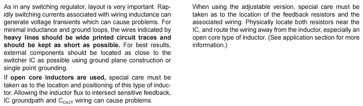
PCB routing based on LM2596S-ADJ requires attention to the following key points:
- High-Current Trace Optimization: The high-current paths marked by thick lines in the diagram shall use wide
PCBtraces and be kept as short as possible to reduce routing inductance and ground loops, thus avoiding voltage transients. - Compactness of Component Layout: External components (such as input and output capacitors, inductors, and diodes) should be placed as close to the chip as possible, and a ground plane or single-point grounding design should be adopted to reduce electromagnetic interference.
- Isolation of feedback circuit: For the adjustable version, the feedback resistor shall be physically placed close to the feedback pin of the chip, and its trace shall be kept away from inductors (especially open-core inductors) to prevent the magnetic flux of the inductor from interfering with the feedback signal and thus affecting the output voltage accuracy.
- Open-core inductor protection: If an open-core inductor is used, its position and placement must be strictly controlled to prevent the inductor's magnetic flux from intersecting with the feedback lines, the chip ground path, and the output capacitor wiring, so as to avoid circuit instability caused by interference.
III. Instructions for Circuit Engineering and Module Usage
3.1 Circuit Source Engineering
To obtain the source code of the circuit, please follow the official account [Freak Embedded]
3.2 Module Usage Instructions
The schematic diagram of this module is shown below:
SCH_Adjustable Power Supply Module Based on LM2596S_v1.0_2025-10-24.pdf 1.9 MB
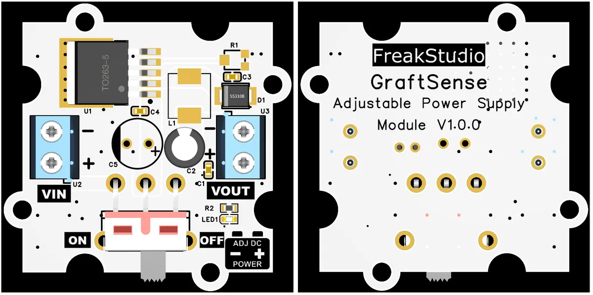
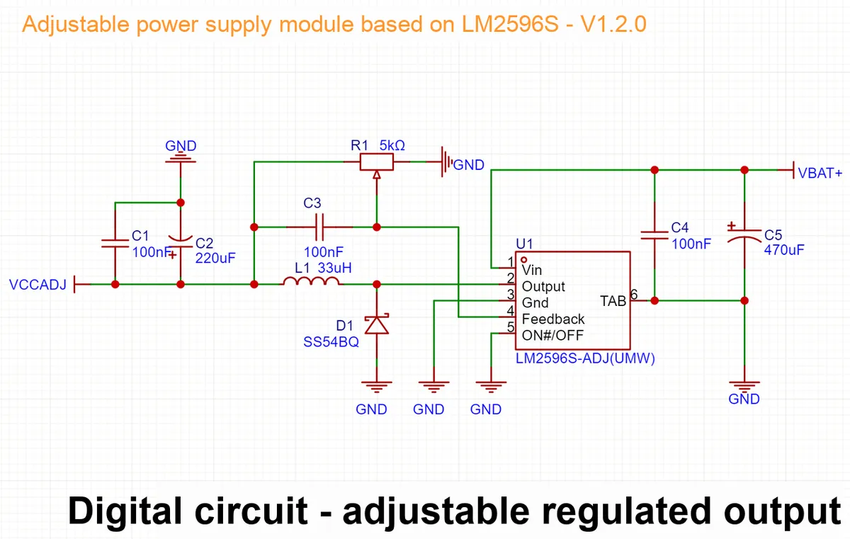
The usage method of this module is as follows:
- Power Input Interface (
VIN): Connect a DC input power supply with a voltage range of 4.5V~40V to theVINinterface in accordance with the interface polarity markings ("+" to the positive pole of the power supply, "-" to the negative pole of the power supply) to supply input power to the module. - Power Output Interface (
VOUT): Connect the load device requiring power supply to theVOUTinterface, ensure the positive and negative polarities are matched; this interface outputs a regulated DC voltage. - Power Adjustment Resistor: The adjustment potentiometer on the rotary module adjusts the output voltage by changing the feedback voltage division ratio, with an output range of 1.23V to 37V, which can be flexibly set according to load requirements.
- Power Switch (
ON/OFF): Toggle the switch; the "ON" position powers on the module for operation, while the "OFF" position cuts off power and puts the module into standby mode, serving to control the power on/off of the module.
3.3 Application Experiment
Here, we use an adjustable power supply module based on the LM2596S connected to a battery for power supply.
The module connections are shown in the following table:
Lithium Battery | Module Pins | Description |
|
| - |
|
| - |
- |
| External power supply interface |
- |
| External power supply interface |
Variable resistor on the screwdriver adjustment module: When adjusting the variable resistor, we can find that the voltage output can be adjusted
IV. Drivers
This module can operate independently without requiring software drivers, so it is not applicable for the time being.
5. BOM & Recommended Alternative Parts
None.
VI. Revision History
Document Version | Date of Revision | Modifier | Revised Content |
v1.0 | 2025-08-13 | Zero Kōkō | Initialize the document |
v1.1 | 2025-10-24 | Li Zisheng | Added PCB layout precautions for Version 2.8 Revised Section 3, Instructions for Circuit Source Project and Module Usage, and added a secondary heading: 3.1 Circuit Source Engineering, 3.2 Module Usage Instructions, 3.3 Application Experiments The BOM sheet has not been finally checked, the driver has not been re-verified, and the 3.3 application experiment Not yet specified. |
v1.2 | 2025-12-29 | Li Zisheng | Added application experiments and production files |
v1.3 | 2025-12-31 | Xin Ruili | Create an open-version document based on the internal document version v1.2. |
VII. Relevant Materials
7.1 Chip Datasheet
LM2596 Datasheet.pdf 3.1 MB
7.2 Unique Icons for PCB Silk Screen