Contents
- I. Module Introduction
- II. Introduction to Major Chips
- 2.1 Chip Overview
- 2.2 Pin Definition
- 2.3 Functional Block Diagram
- 2.4 Performance Parameters
- 2.5 Reference Circuit
- 2.6 Chip Configuration
- 2.7 Communication Interfaces and Related Protocols
- 2.8 PCB Routing Precautions
- III. Circuit Engineering
- 3.1 Circuit Source Engineering
- 3.2 Module Usage Instructions
- 3.3 Application Experiment
- IV. Drivers
- 5. BOM & Recommended Alternative Parts
- VI. Revision History
- VII. Relevant Materials
- 7.1 Chip Datasheet
- 7.2 Unique Icons for PCB Silkscreen
I. Module Introduction
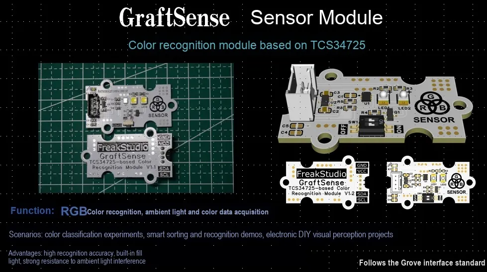
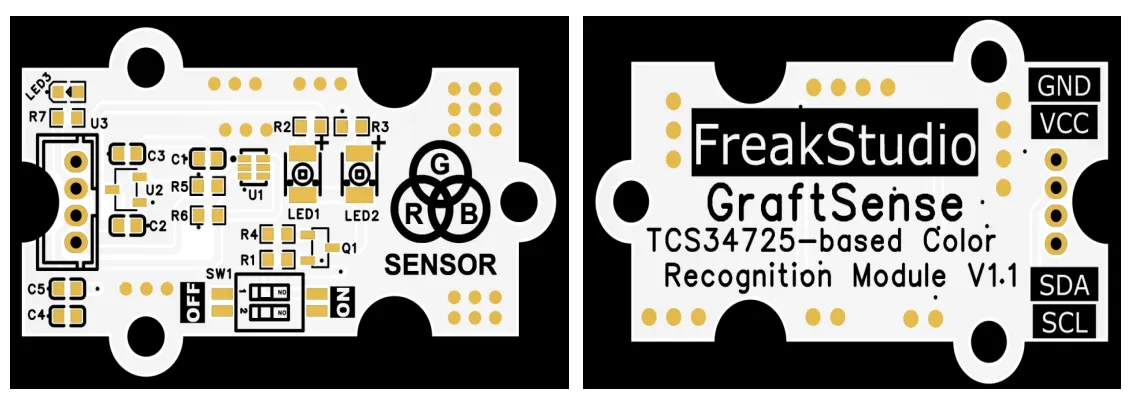
Color recognition module based on TCS34725 takes the TCS34725FN chip as the core, and integrates a color sensor with four channels: red (R), green (G), blue (B) and clear (Clear). It realizes color recognition by detecting light and converting it into digital signals. The module is equipped with a supplementary light control circuit to reduce ambient light interference and improve color measurement accuracy. This module is suitable for scenarios requiring accurate color discrimination such as intelligent recognition and industrial inspection, and provides a reliable hardware solution for color perception applications.
II. Introduction to Major Chips
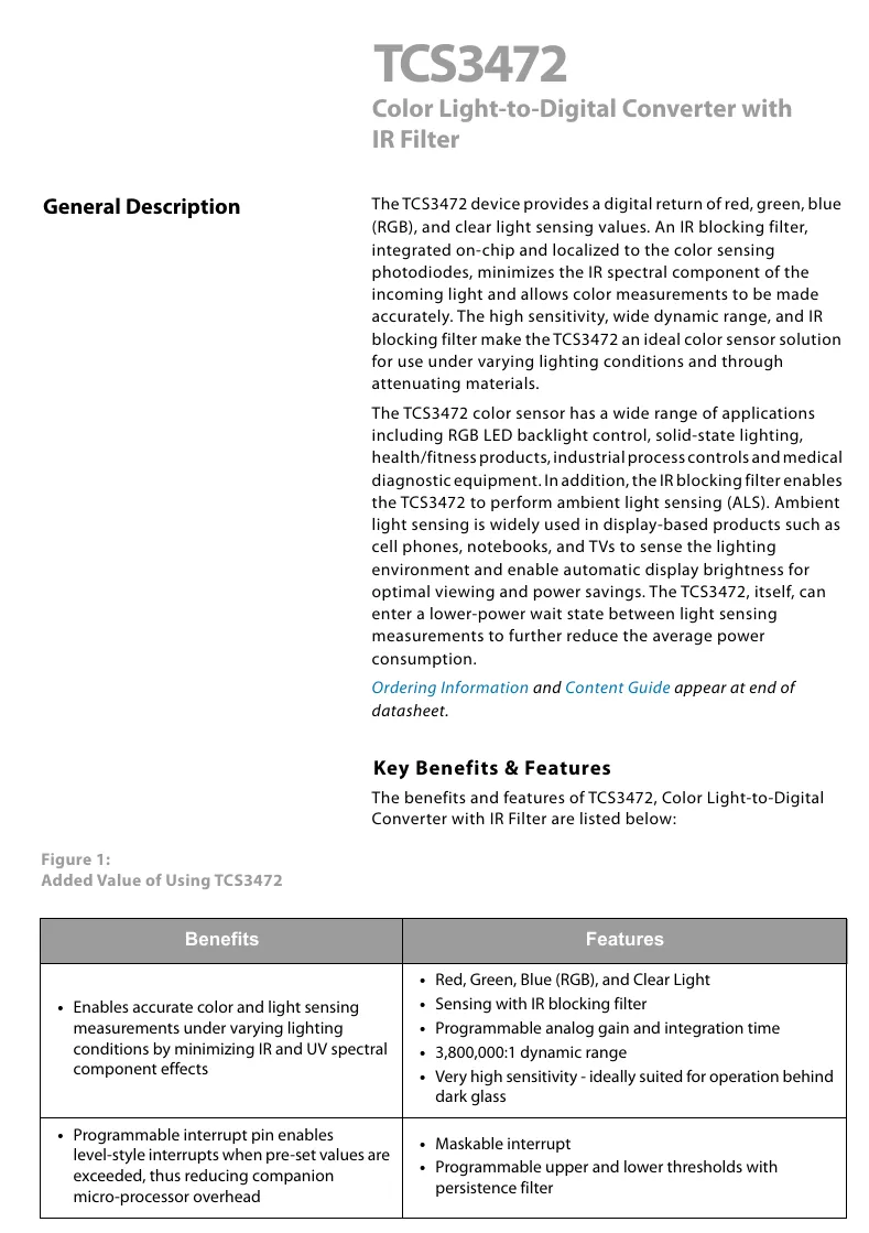
TCS34725 is a high-precision RGB full-color color sensor with a built-in infrared filter and 16-bit ADC. It can accurately detect four light signals including red, green, blue and clear light (Clear), supports the visible light spectrum of 400~700nm, and can output digital color data. Equipped with programmable gain and integration time adjustment functions to adapt to different lighting environments, it communicates with the main controller via the I²C interface, operates on 3.3V power supply with low power consumption (only 0.3μA in standby), features a compact size (2.4mm×2.4mm×0.55mm), complies with the RoHS standard, and is widely used in color recognition, ambient light detection, display calibration, intelligent lighting and other scenarios.
2.1 Chip Overview
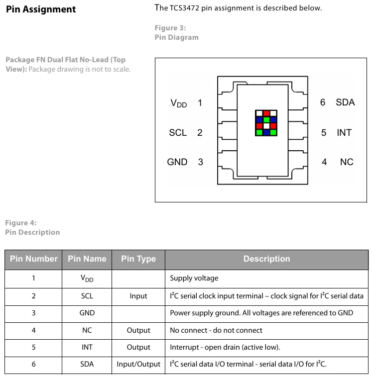
2.2 Pin Definition
2.3 Functional Block Diagram
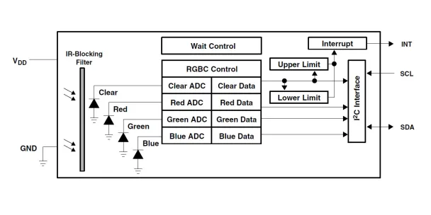
TCS34725 The functional block diagram is described as follows:
- Infrared Filter and Sensing Module
IR-Blocking Filter: Filters infrared light to prevent infrared light from interfering withRGBcolor detection.Clear,Red,Green,Bluephotosensitive units : respectively sense theClear, red, green, and blue light in the environment, convert the light signal into an electrical signal, and provide input for subsequentADconversion.
- Analog-to-Digital Conversion and Data Processing Module
Clear ADC,Red ADC,Green ADC,Blue ADC: These modules perform analog-to-digital conversion on the electrical signals output by theClear, red, green, and blue photosensitive units respectively, converting analog signals into digital signals.Clear Data,Red Data,Green Data,Blue Data: storeADC-converted digital data for subsequent processing or transmission.RGBC Control: controls the detection,RGBandClearchannel detection,ADconversion and data processing procedures, and is the core Control Unit for color detection.
- Control and Interrupt Module
Wait Control: Controls the wait mode of the chip to achieve power consumption management.Upper Limit,Lower Limit: Set the upper and lower limit thresholds for the detection data, which are used to trigger an interrupt.Interrupt: When the detected data exceeds the upper and lower threshold limits, an interrupt signal (INT) is generated to notify the external main controller to perform corresponding processing.
Typical Scenarios for Color Inspection:
- Photosensing and Conversion: After ambient light is filtered by the
IR-Blocking Filter, it irradiates theClear,Red,Green, andBluephotosensitive units → each unit outputs an electrical signal, which is converted into digital data via the correspondingADC. - Data Processing and Interrupt :
RGBC Controlprocesses the converted data → if the data exceeds the threshold set by theUpperLimitorLower Limit→ theInterruptmodule generates anINTinterrupt signal → the external main controller reads the data via theI²C Interfacefor color recognition or exception handling.
2.4 Performance Parameters
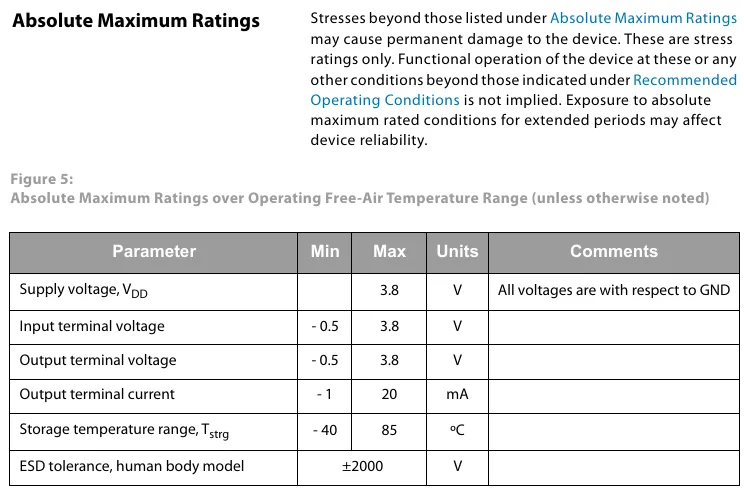
TCS34725 Absolute Maximum Ratings:
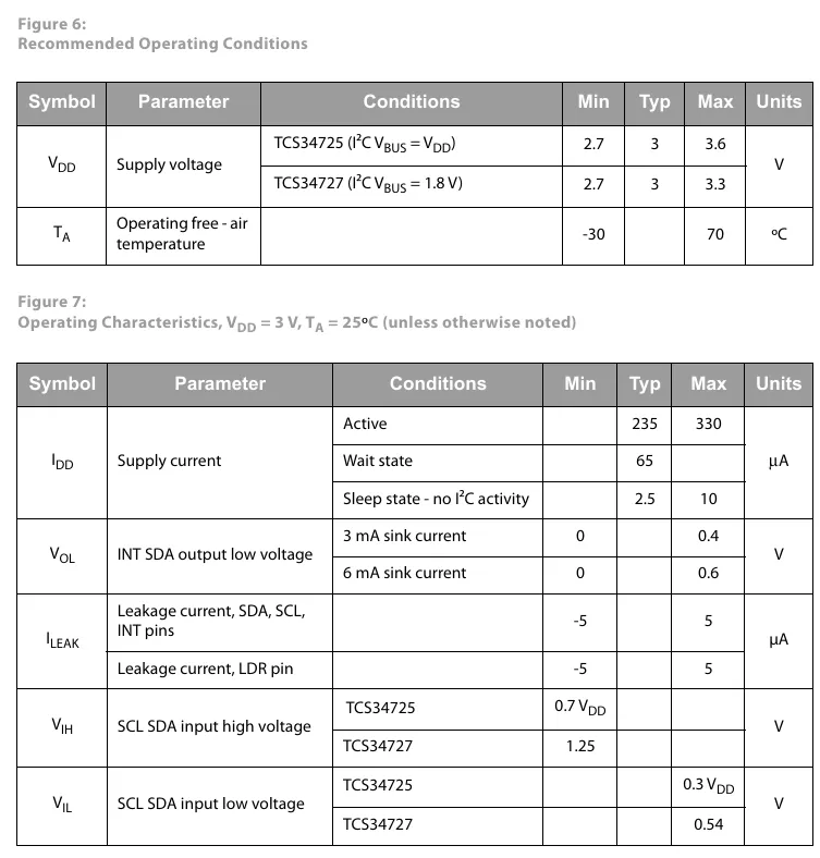
TCS34725 DC Electrical Characteristics Description:
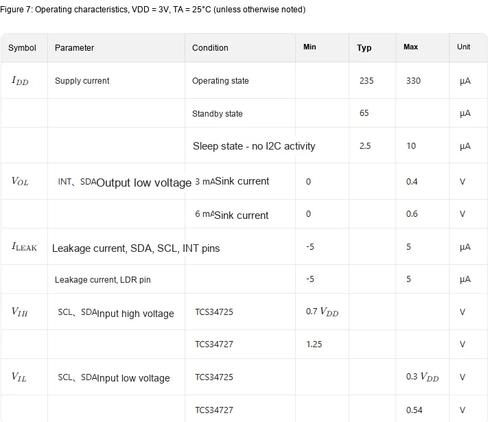
- Power Supply and Voltage:
- Supply Voltage VDD Max. 3.8V;
- Voltage range of input and output terminals: -0.5~3.8V;
- Output terminal current: 1~20mA.
- Environment and Protection:
- Storage temperature range: -40~85℃;
- ESD tolerance (human body model): ±2000V.
- Operating Current:
- Typical operating supply current: 235μA, maximum: 330μA;
- Typical standby current: 65μA;
- Sleep state (no I²C activity): typically 2.5~10 μA.
- Output and Leakage Current:
- INT and SDA output low voltage: maximum 0.4V at 3mA sink current, maximum 0.6V at 6mA sink current;
- Leakage current of SDA, SCL, INT and LDR pins: -5~5μA.
- Input Level:
- When SCL and SDA are input with high voltage, for TCS34725 it is 0.7 VDD, and for TCS34727 it is 1.25V;
- Input low voltage, 0.3V for TCS34725 VDD, and 0.54V for TCS34727.
AC Electrical Characteristics (V DD= 3V, T A= 25℃)
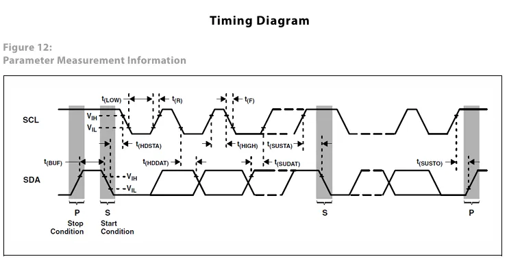
| Parameter | Description | Min | Typ | Max | Unit |
| f(SCL) | Clock frequency (I²C only) | 0 | 400 | kHz | |
| t(BUF) | Bus free time between start and stop conditions | 1.3 | μs | ||
| t(HDSTA) | Hold time after a (repeated) start condition. After this period, the first clock is generated. | 0.6 | μs | ||
| t(SUSTA) | Setup time for a repeated start condition | 0.6 | μs | ||
| t(SUSTO) | Setup time for a stop condition | 0.6 | μs | ||
| t(HDDAT) | Data hold time | 0 | 0.9 | μs | |
| t(SUDAT) | Data setup time | 100 | ns | ||
| t(LOW) | SCL clock low period | 1.3 | μs | ||
| t(HIGH) | SCL clock high period | 0.6 | μs | ||
| tF | Clock/data fall time | 300 | ns | ||
| tR | Clock/data rise time | 300 | ns | ||
| Ci | Input pin capacitance | 10 | pF |
The spectral responsivity plot is shown as follows:
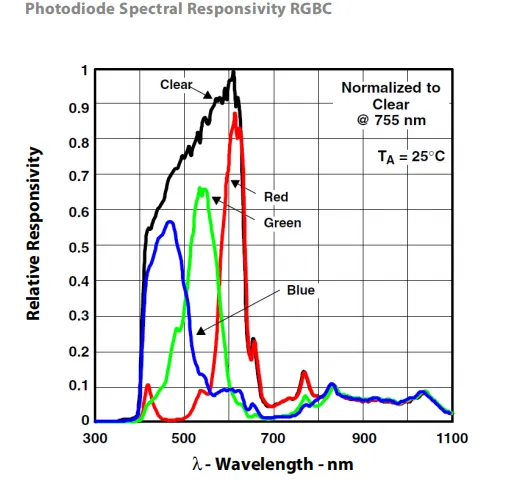
This is the TCS34725 RGBC photodiode spectral response characteristic curve, which illustrates the relative responsivity of its four channels, namely Clear (full transmission), Red (red light), Green (green light), and Blue (blue light), to light with wavelengths ranging from 300 nm to 1100 nm at an ambient temperature of 25°C (normalized with reference to the response of the Clear channel at 755 nm).
The response characteristics of different channels have their own focuses: Clear channel has a wide wavelength coverage in response, while the Red, Green, and Blue channels have more significant responses to the optical bands of their corresponding colors (red, green, and blue bands) respectively. This feature enables the TCS34725 to distinguish light of different wavelengths, thus realizing functions such as color detection and ambient light intensity sensing.
The normalized responsivity and angular displacement diagrams are shown as follows:
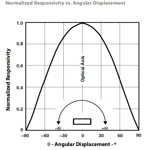
This graph illustrates TCS34725 's response characteristics to light incident angles: when light is incident normally along the sensor' s optical axis (angular displacement of 0°), its normalized responsivness reaches the maximum (close to 1.0); as the incident angle shifts towards ±90°, the responsivness gradually decreases, and drops to 0 at ±90°. This characteristic indicates that TCS34725 has the optimal detection sensitivity for normally incident light, and the greater the deviation of the incident angle, the lower the detection sensitivity. In practical applications, the light should be kept as close to normal incidence as possible to ensure the accuracy of color and light intensity detection.
2.5 Reference Circuit
None.
2.6 Chip Configuration
None.
2.7 Communication Interfaces and Related Protocols
2.7.1 IIC Communication Protocol
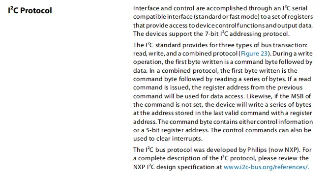
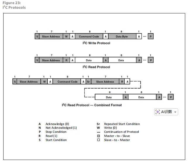
This section describes the TCS34725 I²C Communication Protocol function: it controls registers via an interface compatible with I²C (Standard / Fast Mode) to achieve device control and data output, and supports 7-bit I²C addresses.
I²C includes three types of bus transactions: write protocol, read protocol, and combined protocol.
The command byte can carry control information or a 5-bit register address; control commands can also clear interrupts. For read operations, the register address corresponding to the previous command is reused, and if no address is set, the register address of the last valid command is used.
2.7.2 Register Description
2.7.2.1 Command Register
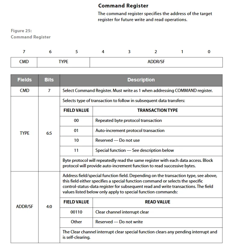
This is an 8-bit command register that is used to control the transaction type and function selection for subsequent data transmission, and it is divided into 3 fields:
- CMD (Bit 7): Used to select the command register; this bit must be set to 1 when accessing this register.
- TYPE (bits 6-5): Specifies the transaction type for subsequent data transmission, including "Repeat Byte Protocol Transfer (00)" and "Auto-increment Protocol Transfer (01)"; 10 is reserved, and 11 corresponds to a special function.
- ADDR/SF (Bits 4-0): Functions as an address field or a special function field depending on the transaction type; for special functions, only "00110" corresponds to the "clear channel interrupt" function, and all other values are reserved.
The core function of this register is to coordinate the interaction mode of subsequent read and write transactions, and it also supports special functions such as interrupt clearing.
2.7.2.2 Enable Register
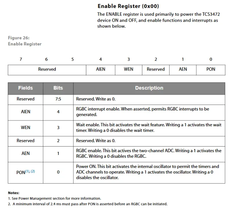
The TCS3472's enable register (address 0x00) is primarily used to control the device's power supply, function activation, and interrupt switch:
- Field distribution: includes reserved bits (bits 7-5 and bit 2, which must be written as 0), AIEN (bit 4), WEN (bit 3), AEN (bit 1), and PON (bit 0).
- Function of each field:
- AIEN: Set to 1 to enable RGBC interrupt;
- WEN: Set to 1 to enable the wait timer, set to 0 to disable it;
- AEN: Set to 1 to activate the dual-channel ADC of RGBC, set to 0 to disable it;
- PON: Set to 1 to activate the internal oscillator (to enable the timer and ADC to operate), set to 0 to power off the device; note that after PON is set to 1, wait for at least 2.4ms before enabling the RGBC function.
2.7.2.3 RGBC Timing Register
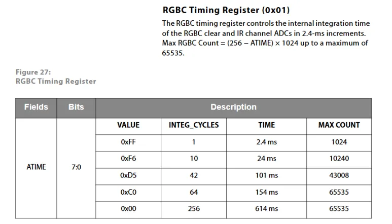
The TCS3472 RGBC Timing Register (address 0x01) is primarily used to control the integration time of the RGBC and IR channel ADCs (in steps of 2.4ms):
- The field is
ATIME(occupies bits 7 to 0), and differentATIMEvalues correspond to different integration parameters: the maximum count (upper limit 65535) is calculated via(256 - ATIME) × 1024, which also corresponds to different integration cycles and durations; for example,0xFFcorresponds to 1 cycle, 2.4ms integration time, and a maximum count of 1024;0x00corresponds to 256 cycles, 614ms integration time, and a maximum count of 65535. - This register can adapt to the RGBC detection sensitivity and measurement range under different brightness scenarios by adjusting the integration time.
2.7.2.4 Wait Time Register
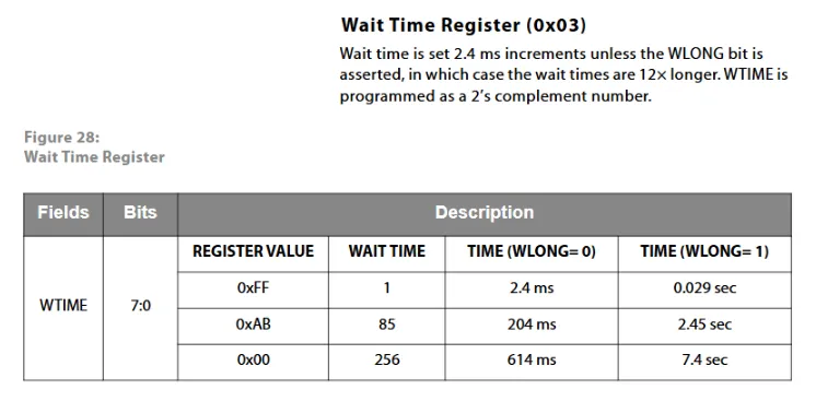
The TCS3472 Wait Time Register (address 0x03) is primarily used to configure the waiting duration of the device:
- Contains only the
WTIMEfield (occupying bits 7 to 0), with the basic step of waiting time being 2.4ms; ifWLONGis at position 1, the waiting time will be amplified by 12 times, andWTIMEis programmed in two's complement form. - Different
WTIMEvalues correspond to different waiting parameters: for example,0xFFcorresponds to 1 waiting cycle, whenWLONG= 0the waiting time is 2.4ms, and whenWLONG= 1the waiting time is 0.029 seconds;0x00corresponds to 256 cycles, whenWLONG= 0the waiting time is 614ms, and whenWLONG= 1the waiting time is 7.4 seconds. - This register can flexibly adjust the waiting timing of the device to adapt to the requirements of detection intervals in different scenarios.
2.7.2.5 RGBC Interrupt Threshold Register Bank
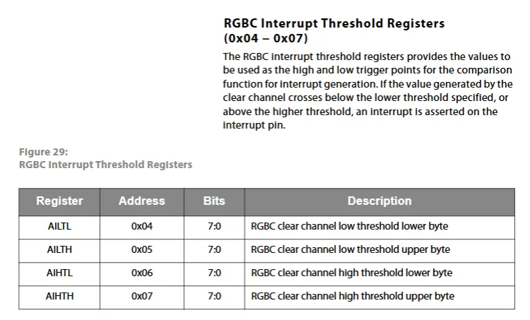
The TCS3472's RGBC interrupt threshold register bank (addresses 0x04–0x07) is primarily used to set the high and low trigger thresholds for interrupts:
- Function: Provides high and low trigger points for the interrupt comparison function. When the measured value of the clear channel is lower than the low threshold or higher than the high threshold, an interrupt on the interrupt pin will be triggered.
- Contains 4 8-bit registers:
- AILTL (0x04): The low byte of the RGBC clear channel low threshold;
- AILTH (0x05): The high byte of the low threshold for the RGBC clear channel;
- AIHTL (0x06): the low byte of the high threshold for the RGBC clear channel;
- AIHTH (0x07): RGBC clear channel high threshold high byte; these four registers together form the 16-bit low threshold and high threshold, enabling flexible configuration of interrupt trigger conditions.
2.7.2.6 Persistent Register
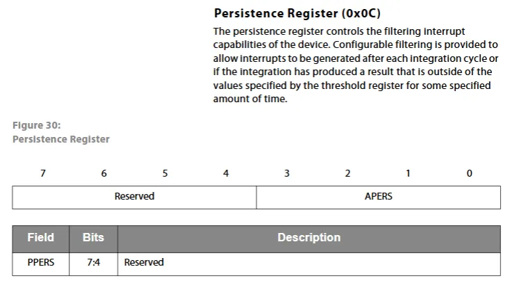
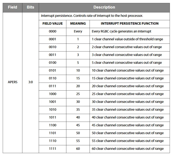
The Persistent Register (address 0x0C) of the TCS3472 is primarily used to control the filter trigger conditions for interrupts so as to reduce spurious interrupts:
- Register structure: Bits 7-4 are reserved bits (PPERS), and bits 3-0 correspond to the
APERSfield, which is responsible for configuring the interrupt hold function. - Function logic: By using
different values of APERS, it sets "how many consecutive times the clear channel measurement value exceeds the threshold before an interrupt is triggered" — for example,0000corresponds to triggering an interrupt every RGBC cycle,0001corresponds to triggering once the threshold is exceeded 1 time,1111corresponds to triggering only after 60 consecutive threshold exceedances. - Function: It controls the trigger frequency of interrupts sent to the host. By setting the number of consecutive times that the threshold is exceeded, it filters out false interrupts caused by single abnormal values, so as to adapt to the stability requirements of different scenarios.
2.7.2.7 Configuration Register
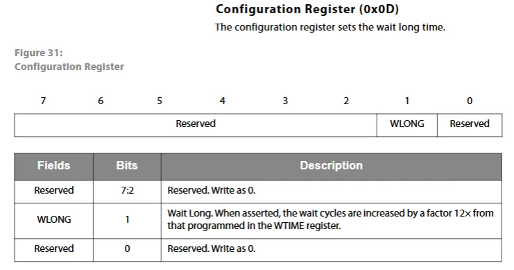
The configuration register of the TCS3472 (address 0x0D) has the core function of controlling the amplification factor of the waiting duration:
- Register structure: bits 7-2 and bit 0 are reserved bits (must be written as 0), and only bit 1 is the
WLONGfield. - Function logic: When
WLONGis at position 1, the wait cycles set in the Wait Time register (WTIME) will be amplified 12 times, so as to expand the adjustable range of waiting time and cooperate with the WTIME register to realize more flexible waiting timing configuration.
2.7.2.8 Control Register
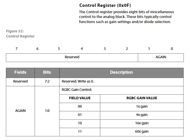
The TCS3472 control register (address 0x0F) is primarily used to configure the analog gain of the RGBC channels:
- Register structure: Bits 7 to 2 are reserved bits (must be written as 0), and bits 1 to 0 are the
AGAINfield, which is responsible for RGBC gain control. - Gain configuration logic:
AGAINdifferent values correspond to different gain multiples — 00 stands for 1x gain, 01 for 4x gain, 10 for 16x gain, and 11 for 60x gain. - Function: By adjusting the analog gain of the RGBC channels, it adapts to the signal acquisition requirements of different brightness environments (e. g., high gain for dark environments and low gain for bright environments) to ensure the accuracy of color detection data.
2.7.2.9 ID Register
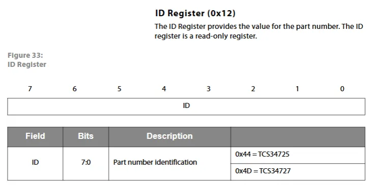
The TCS3472 ID register (address 0x12) is a read-only register that is primarily used to identify the device model:
- The register only contains
IDfield (occupies bits 7 to 0), which functions as the device model identifier; - Different ID values correspond to different models: 0x44 stands for TCS34725, and 0x4D stands for TCS34727. The model of the sensor in use can be confirmed by reading the value of this register.
2.7.2.10 Status Register
The TCS3472's status register (address 0x13) is a read-only register used to report the internal operating status of the device:
- Register field distribution: bits 7-5 and bits 3-1 are reserved bits;
- Valid Field Function:
AINT(Bit 4): Indicates that RGBC clears the interrupt status of the channel;AVALID(Bit 0): Indicates that the RGBC channel has completed one integration cycle, and the corresponding detection data is valid.
2.7.2.11 RGBC Channel Data Register Bank
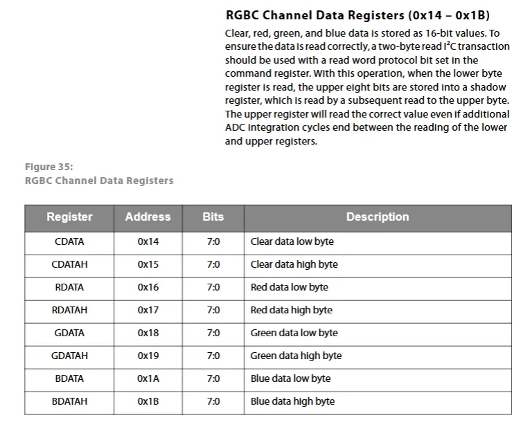
The TCS3472's RGBC channel data register set (addresses 0x14–0x1B) is primarily used to store 16-bit light detection data:
- Function: Save the detection data of Clear, Red, Green and Blue; the data of each channel is 16 bits, which is represented by the combination of "low-byte register + high-byte register";
- Correspondence of each register: For example, CDATA (0x14) is the register for clearing the low byte of light, CDATAH (0x15) is the register for clearing the high byte of light, and the R/G/B channels also correspond to their respective low-byte (RDATA/GDATA/BDATA) and high-byte (RDATAH/GDATAH/BDATAH) registers;
- Reading requirement: The data shall be read via an I2C two-byte read transaction (word read protocol). After the low byte is read, the high byte will be stored in the shadow register, which ensures that the data is correct when the high byte is read subsequently, and this will not be affected even if the ADC integration cycle ends during the read-write process.
2.8 PCB Routing Precautions
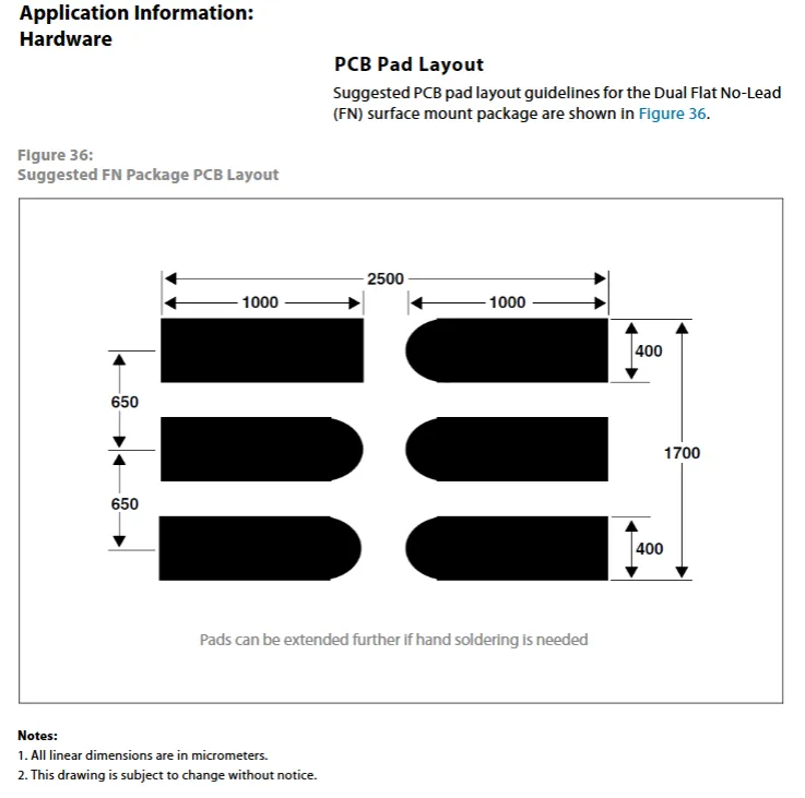
This is the PCB pad layout guide in the hardware application information for TCS3472 (FN package), which provides the recommended PCB pad design scheme for the dual no-lead flat (FN) surface-mount package:
- Layout and Dimensions: The unit of measurement for dimensions is micrometer. The pads are divided into two groups on the left and right, with a total width of 2500μm and an overall height of 1700μm; the pads feature various shapes (such as structures with a semicircular end), and parameters including the spacing between individual pads (e. g., 650μm) and partial lengths (e. g., 1000μm) have been marked.
- Practical Instructions: If manual soldering is adopted, the solder pads can be further extended to facilitate the operation.
- Notes: All linear dimensions are in micrometers, and this drawing is subject to change without notice.
This layout serves as a reference design for the surface-mount assembly of FN packaged devices on PCBs, ensuring the soldering reliability and compatibility of the devices.
III. Circuit Engineering
3.1 Circuit Source Engineering
To obtain the source project of the circuit, please follow the official account [Freak Embedded]
3.2 Module Usage Instructions
SCH_Schematic1_TCS34725-Based Color Recognition Module-V1.1.0_2025-11-12.pdf 2.1 MB
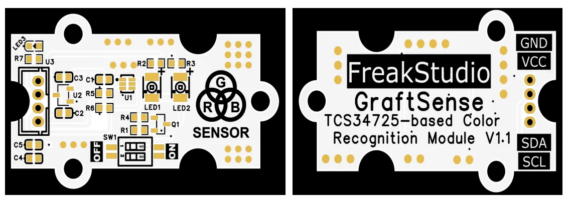
This module provides an I2C communication interface: it supports standard I2C communication rate, with a default I2C address of 0x29, is compatible with 3.3V/5V logic levels, and can stably transmit the four-channel digital color data of the TCS34725 RGBC sensor. Meanwhile, it can send fill light control commands through this interface to reduce ambient light interference. It is suitable for scenarios such as color recognition in maker projects, color perception of smart devices, and color identification in industrial inspection, providing accurate digital signal interaction capabilities for color perception applications.
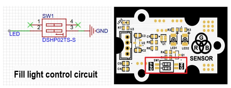
If the detection environment is relatively dark, you can toggle the following DIP switch to turn on the fill light circuit to improve the detection effect.
3.3 Application Experiment
Here, we use the GraftPort-RP2040 development board for testing, and connect the TCS34725-based color recognition module to communicate with the main controller via the I2C interface.
Here, we first use the HY2.0-4P cable to connect the module to the GraftPort-RP2040 development board's I2C0 interface:
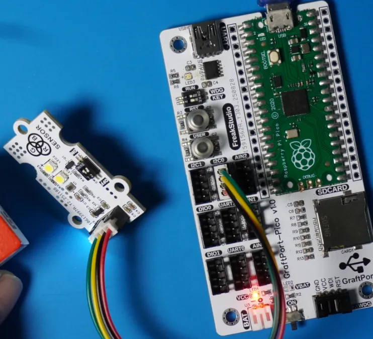
The module connections are shown in the following table:
Development Board Pins | Module Pins | Description |
Pin 4 |
|
|
Pin 5 |
|
|
Here, we need to search for the relevant driver packages on uPyPI: https://upypi.net/zh/
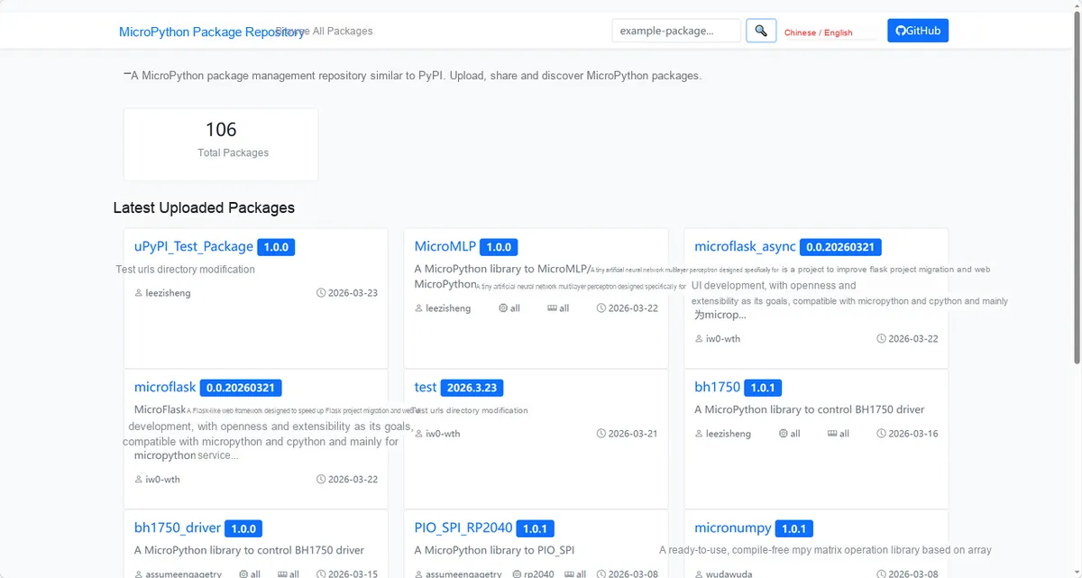
Enter tcs34725_color_driver to search, and the following will be displayed:

Click to copy the local installation command:
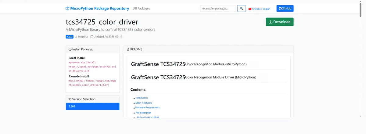
Here, we can use the mip tool to import module driver library code. The following are the usage commands for the mpremote tool:
mpremote mip install github:FreakStudioCN/GraftSense-Drivers-MicroPython/sensors/tcs34725_color_driverImport the TCS34725-based color recognition module - MicroPython driver code, then copy the following main.py code into our project:
# Python env   : MicroPython v1.23.0
# -*- coding: utf-8 -*-
# @Time    : 2024/9/1 2:10 PM
# @Author  : Li Qingshui
# @File    : main.py
# @Description : DAC experiment, using an external DAC chip to generate a sine waveform

# ======================================== Import Modules ========================================

# Import the hardware module
from machine import ADC, Timer, Pin, I2C, UART
# Import time-related modules
import time
# Import the module for accessing and controlling MicroPython internals
import micropython
# Import the math library for calculating the sine wave
import math
# Import the mcp4725 module to control the DAC chip
from mcp4725 import MCP4725

# ======================================== Global Variables ============================================

# mcp4725 chip address
DAC_ADDRESS = 0x00
# Voltage conversion factor
adc_conversion_factor = 3.3 / (65535)

# ======================================== Functions ============================================

# Timer callback function
def timer_callback(timer: Timer) -> None:
    """
    Timer callback function, used to read ADC data periodically and call the user-defined callback function.

    Args:
        timer (machine.Timer): Timer instance.

    Returns:
        None
    """

    # Declare global variables
    global adc,adc_conversion_factor

    # Read ADC data
    value = adc.read_u16() * adc_conversion_factor
    # Call the user-defined callback function
    micropython.schedule(user_callback, (value))

# User-defined callback function
def user_callback(value: float) -> None:
    """
    User-defined callback function, used to process the voltage value sampled by the ADC and send it over the serial port.

    Args:
        value (float): Voltage value sampled by the ADC.

    Returns:
        None
    """
    # Declare global variables
    global uart

    # Get the floating-point number and round it to two decimal places
    formatted_value = "{:.2f}".format(value)
    # Send the sampled voltage data over the serial port
    uart.write(str(formatted_value) + '\r\n')
    # Print the sampled voltage data to the terminal
    print('dac generated voltage: ' + str(formatted_value))

# ======================================== Custom Classes ============================================

# ======================================== Initialization ==========================================

# Delay 3 s to wait for the device to finish powering up
time.sleep(3)
# Print debug information
print("FreakStudio : Using DAC to generate sine wave")

# Create a hardware I2C instance using the I2C1 peripheral, with a clock frequency of 400KHz, SDA pin 4, and SCL pin 5
i2c = I2C(id=0, sda=Pin(4), scl=Pin(5), freq=400000)

# Start scanning for devices on the I2C bus and return a list of slave addresses
devices_list = i2c.scan()
print('START I2C SCANNER')

# If devices_list is empty, no device is connected to the I2C bus
if len(devices_list) == 0:
    print("No i2c device !")
# If not empty, print the slave device addresses
else:
    print('i2c devices found:', len(devices_list))
    # Iterate over the slave device address list
    for device in devices_list:
        # If the device address is between 0x60 and 0x61, it is a DAC chip
        if 0x60 <= device <= 0x61:
            print("I2C hexadecimal address: ", hex(device))
            DAC_ADDRESS = device

# Create the DAC object, using the I2C0 peripheral, with address DAC_ADDRESS
dac = MCP4725(i2c, DAC_ADDRESS)
# Read the DAC configuration information
eeprom_write_busy, power_down, value, eeprom_power_down, eeprom_value = dac.read()
print(eeprom_write_busy, power_down, value, eeprom_power_down, eeprom_value)
# Configure the DAC: cancel power-down mode, output voltage 0V, write to EEPROM
dac.config(power_down='Off',value=0,eeprom=True)
# Delay 50ms; reading immediately after configuration causes an error
time.sleep_ms(50)
# Read the DAC configuration information
eeprom_write_busy, power_down, value, eeprom_power_down, eeprom_value = dac.read()
print(eeprom_write_busy, power_down, value, eeprom_power_down, eeprom_value)

# Create the ADC instance: ADC1-GP27
adc = ADC(1)
# Create a software timer object
timer = Timer(-1)
# Start the timer, triggering the timer_callback function every 5ms to sample voltage with the ADC
timer.init(period=5, mode=Timer.PERIODIC, callback=timer_callback)

# Create the serial port object, set the baud rate to 115200
uart = UART(0, 115200)
# Initialize the uart object with a baud rate of 115200, 8 data bits, no parity bit, and 1 stop bit
# Set the serial port timeout to 100ms
uart.init(baudrate  = 115200,
          bits      = 8,
          parity    = None,
          stop      = 1,
          tx        = 0,
          rx        = 1,
          timeout   = 100)

# ========================================  Main Program  ===========================================

# Generate the sine wave
for i in range(10000):
    # Calculate the voltage value of the sine wave
    value = 3.3 * math.sin(2 * math.pi * i / 100) + 3.3
    # Convert the voltage value of the sine wave to an integer
    value = int(value * 4095 / 6.6)
    # Write the analog value to the DAC
    dac.write(value)
    # Delay 10ms
    time.sleep_ms(10)

# Stop ADC sampling
timer.deinit()
Burn the code, open the terminal, and use the mpremote tool to connect to the main controller. The output is as follows:
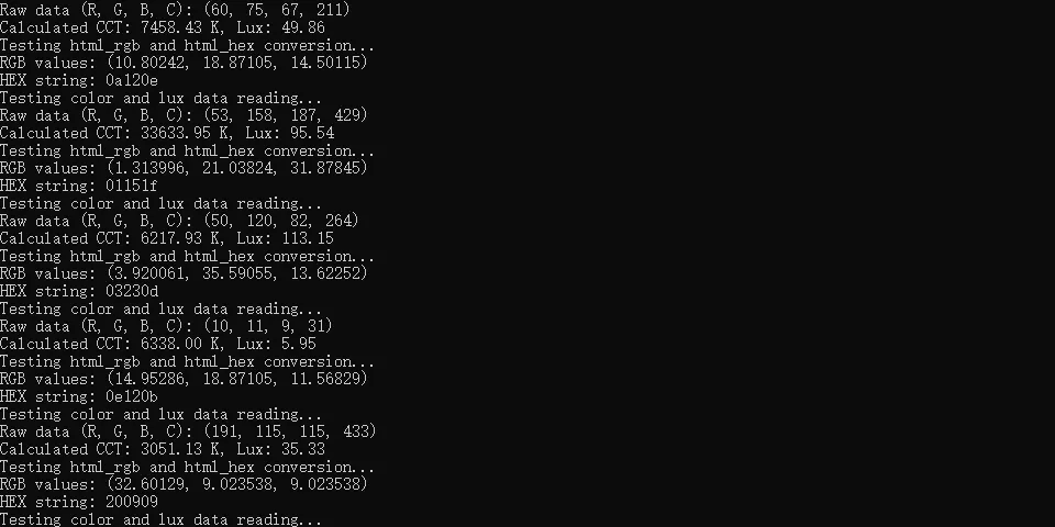
It can be seen that when we move color blocks of different colors such as red, green, blue and yellow close to the module, the terminal will output the corresponding different color component values and the corresponding color codes:
IV. Drivers
tcs34725_color_driver.zip 14 KB
5. BOM & Recommended Alternative Parts
None.
VI. Revision History
Document Version | Date of Modification | Modifier | Modified Content |
v1.0 | 2025-11-12 | Ling Gaoxing | Initialize the document |
v1.1 | 2025-12-29 | Li Zisheng | Added application experiments and production files |
v1.2 | 2025-12-31 | Xin Ruili | Create an open version of the document based on the internal document version v1.1. |
v1.3 | 2026-03-29 | Xin Ruili | Modified the application experiment section |
VII. Relevant Materials
7.1 Chip Datasheet
TCS34725FN Datasheet.pdf 1.5 MB
7.2 Unique Icons for PCB Silkscreen