
Contents
- I. Module Introduction
- II. Introduction to Major Chips
- 2.1 Chip Overview
- 2.2 Pin Definition
- 2.3 Functional Block Diagram
- 2.4 Performance Parameters
- 2.5 Reference Circuit
- 2.6 Chip Configuration
- 2.7 Communication Interfaces and Related Protocols
- 2.8 PCB Routing Precautions
- III. Circuit Engineering
- 3.1 Circuit Source Engineering
- 3.2 Module Usage Instructions
- 3.3 Application Experiment
- IV. Drivers
- 5. BOM & Recommended Alternative Parts
- VI. Revision History
- VII. Relevant Materials
- 7.1 Chip Datasheet
- 7.2 Unique Icons for PCB Silkscreen
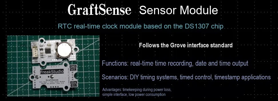
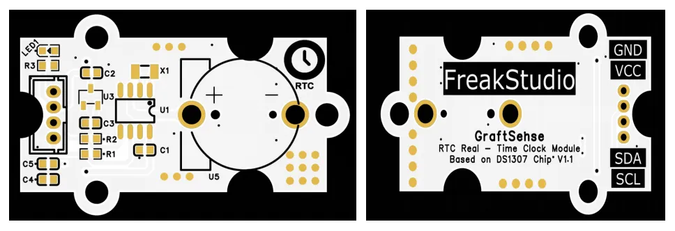
I. Module Introduction
RTC real-time clock module based on DS1307 chip, which adopts the DS1307ZN+ T&R real-time clock chip. This module is equipped with 56 bytes of RAM, featuring a low-power battery operating current of 200uA and an operating current of 1.5mA; if powered by a 48mAh lithium battery, it can operate for ten years at 25°C. It is suitable for various embedded devices requiring precise time recording, and provides reliable real-time clock functionality for the system.
II. Introduction to Major Chips
DS1307 is a low-power real-time clock (RTC) chip that supports complete time data recording including seconds, minutes, hours, date, month, day of week and year, and features an automatic leap year correction function compatible with dates up to the year 2100. It communicates with the main controller via the I²C interface, supports a main power supply of 4.5V~5.5V and a backup power supply of 2.0V~3.0V, has a built-in 32.768kHz crystal oscillator with high time accuracy, adopts a compact package and requires simple peripheral circuits, and is widely used in scenarios requiring precise timing such as smart devices, industrial control and electronic instruments.
2.1 Chip Overview
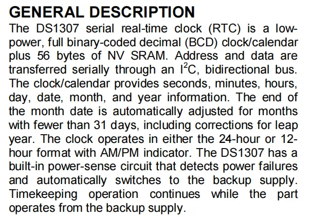
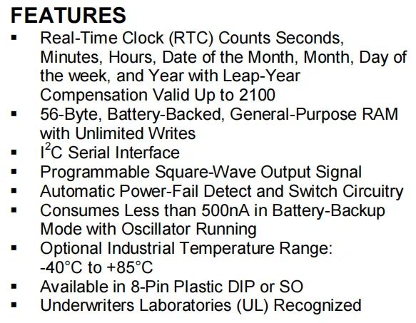
DS1307 is a low-power serial real-time clock (RTC) that integrates a clock/calendar in BCD format (providing information such as seconds, minutes, hours, date, month, and year, with automatic end-of-month date and leap year correction, and support for 12/24-hour mode) and 56-byte battery-backed general-purpose SRAM, and transmits data via the I2C bidirectional bus;It features programmable square wave output, power failure detection and backup power switching (capable of maintaining timing during power outages), draws less than 500nA in backup mode, supports the industrial temperature range from -40°C to + 85°C, comes in an 8-pin package and is UL certified, making it ideal for applications requiring accurate timing and data backup.
2.2 Pin Definition
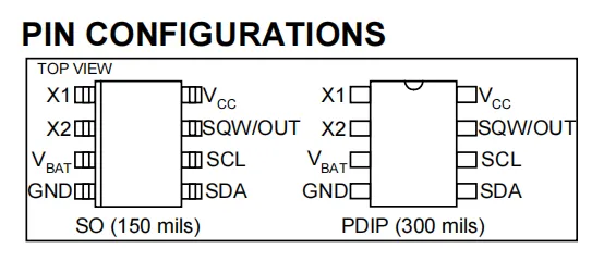
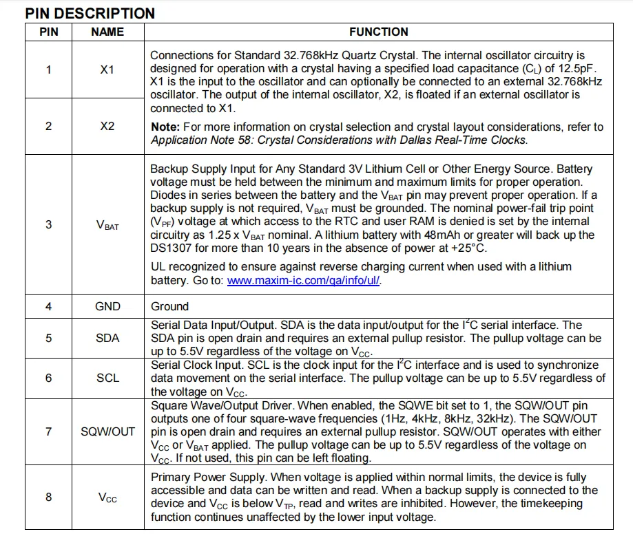
2.3 Functional Block Diagram
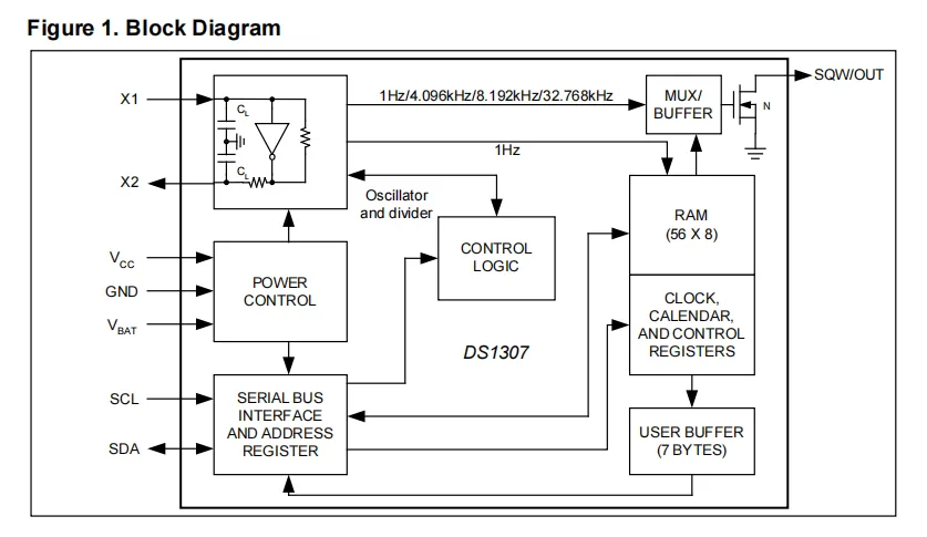
DS1307 The functional architecture of the real-time clock is analyzed as follows: First, the external crystal oscillators connected to X1 and X2 cooperate with the internal oscillator to generate clock signals, which are then divided by the frequency divider to obtain multiple frequency levels such as 1Hz and 4.096kHz; the power supply control module is connected to VCC, GND and VBAT, responsible for detecting the main power supply and automatically switching to the backup power supply to maintain timing when power is off; the serial bus interface implements I2C communication through the SCL and SDA pins to handle address and data transmission;As the core coordination unit, the control logic connects the clock/calendar registers (which store time information such as seconds, minutes, and hours), the 56-byte RAM (for general-purpose data backup), and the 7-byte user buffer; the frequency-divided signal is selected via a multiplexer buffer and outputs a square wave with an optional frequency from the SQWOUT pin, and the whole system realizes the functional coordination of timekeeping, data storage, communication and signal output.
2.4 Performance Parameters
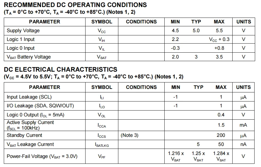
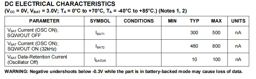
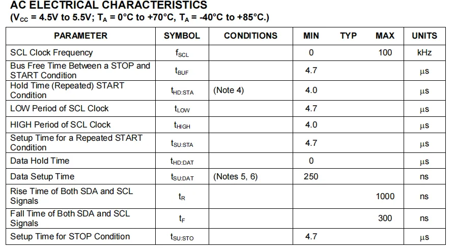
The performance parameters of the DS1307 are mainly determined by the operating voltage, operating current and communication rate, and a brief introduction to these aspects will be given below:
DS1307is equipped with a main power supply and a backup power supply. The main power supplyVCChas a voltage range of 4.5-5.5V (typically 5V), the backup batteryVBAThas a voltage range of 2.0-3.5V (typically 3V), and the logic input levels must meet the requirements ofVIH≥ 2.2V andVIL≤ 0.8V.- Regarding operating current: the typical current is 1.5mA during normal operation, 200μA in standby mode, and when the oscillator is running in backup mode and
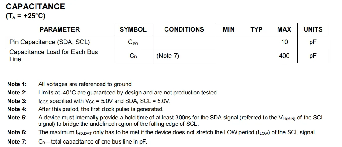
SQWOUTis off, the typical current is 300nA (max. 500nA); when only data retention is active, the typical current is 10nA (max. 100nA), and the maximum input and I/O leakage current is 1μA. DS1307'sIICcommunication rate is up to 100kHz , and it needs to match the bus idle time 4.7μs and other timing parameters. The typical capacitance of the SDA/SCL pin is 10pF, and the maximum capacitance load of a single bus line is 400pF to ensure communication stability.
2.5 Reference Circuit
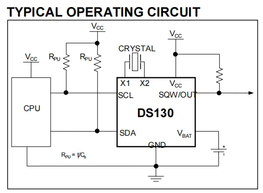
DS1307 reference circuit analysis is as follows: CPU through SCL , SDA pins and DS1307 connection, two pins of external pull-up resistor ( RPU ) for maintaining the I2C bus high level, to ensure the stability of bidirectional communication; DS1307 of X1 , X2 pins connected to the crystal oscillator, providing a reference frequency for real-time clock timing; VBAT terminal connected to the backup battery, the main power supply VCC normal power supply by VCC for the module power supply, when VCC power off, The circuit automatically switches to battery power to maintain clock timing and data storage.The SQW/OUT pin can output external signals after being connected to a pull-up resistor; the entire circuit is powered by the main power supply via VCC and GND, and cooperates with various components to implement the communication, real-time timing and power-off backup functions between the CPU and DS1307.
2.6 Chip Configuration
None.
2.7 Communication Interfaces and Related Protocols
2.7.1 Clocks and Calendars
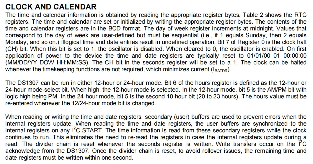
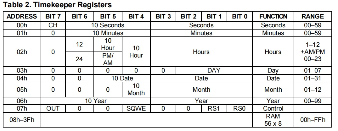
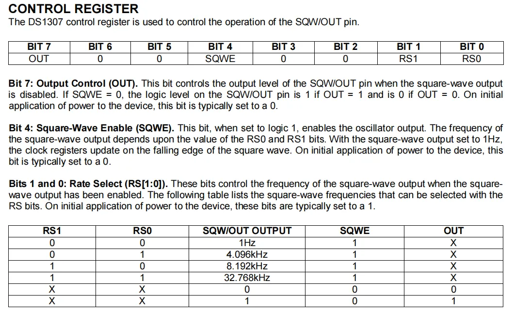
The foregoing content respectively describes DS1307 the configuration procedures for setting the clock, calendar and control registers, and the relevant content is summarized as follows:
DS1307 clock and calendar settings are implemented based on reading and writing registers in BCD format: time (seconds, minutes, hours) and calendar (day, date, month, year) information correspond to the registers at addresses 00h-06h respectively, and BCD code data needs to be written to these registers to initialize or modify the time;The BIT7 ( CH bit) of the second register is the clock start-stop control bit. Setting to 1 will disable the oscillator (clock pause). Setting to 0 will enable it. When initialized, the time is usually reset to 01/01/01 00:00:00 and CH is set to 1. Setting to 1 when not in use can reduce power consumption.
The BIT6 of the hour register BIT6 is used to select the 12/24-hour format: when set high, it is the 12-hour format (BIT5 serves as the AM / PM bit, and a high level indicates PM); when set low, it is the 24-hour format (BIT5 serves as the tens digit for hours 20-23). After switching the mode, the hour value must be re-entered. When reading from or writing to the time register, the internal data is synchronized with the help of a user buffer; during a read operation, the buffer is synchronized when the I2C START signal is triggered to avoid errors caused by internal register updates;Writing to the seconds register will reset the frequency division chain, and the remaining time registers must be written to within 1 second to prevent time overflow.
DS1307 whose control register (corresponding to address 07h) is primarily responsible for managing the output status of the SQW / OUT pin: it controls the enabling/disabling of square wave output via BIT4 (the SQWE bit, set to 1 to enable, 0 to disable); and selects the output frequency of the enabled square wave via BIT1-0 (the RS1 and RS0 bits, with selectable levels including 1Hz, 4.096kHz, etc.);When the square wave is disabled via BIT7 (the OUT bit), this bit sets the fixed level of the SQW / OUT pin (1 for high level, 0 for low level), so as to realize flexible configuration of the output signal.
2.7.2 IIC Data Bus
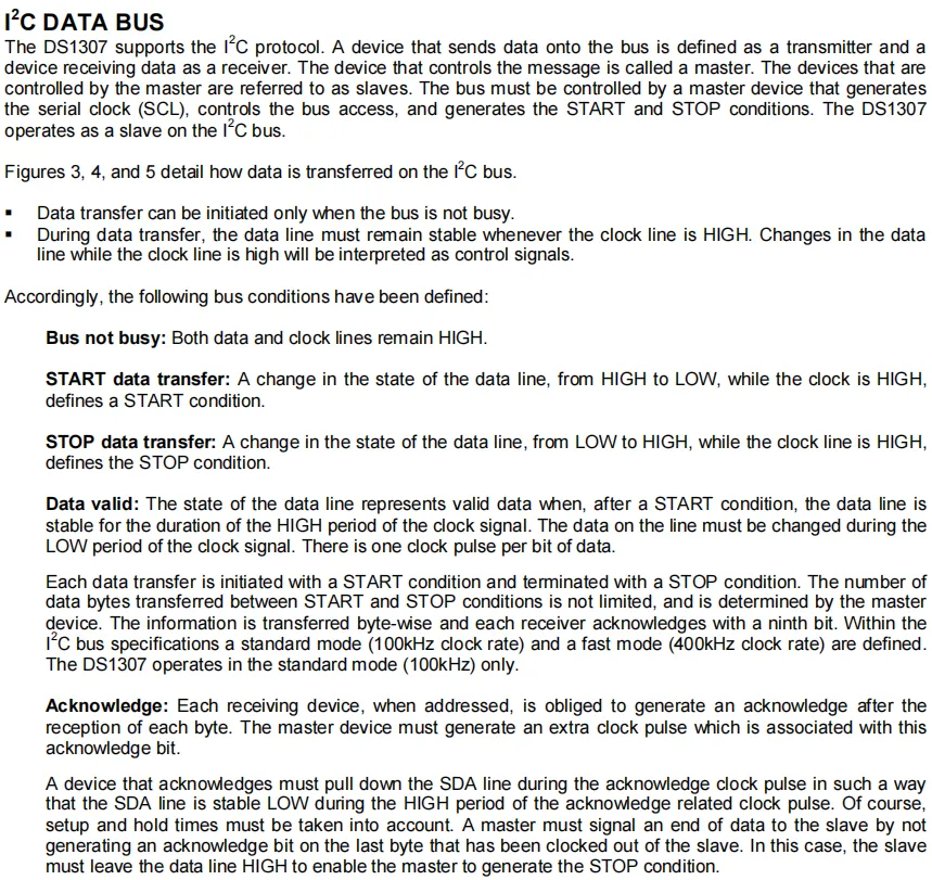
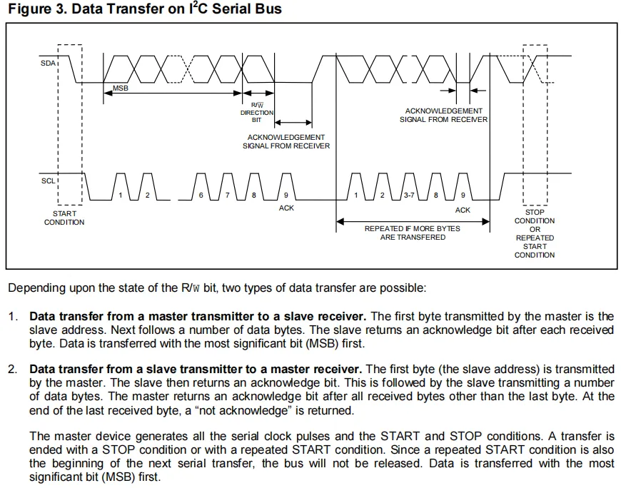
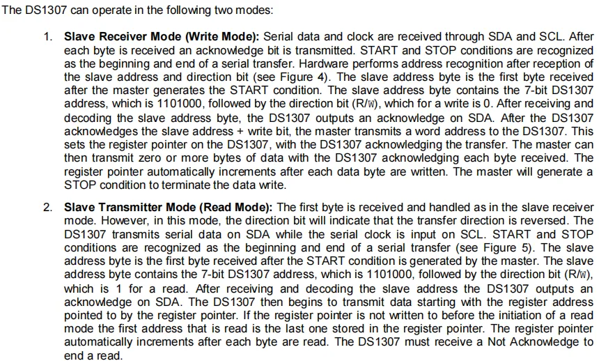
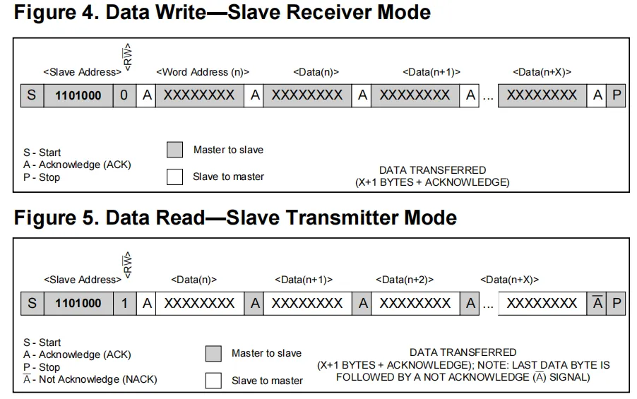
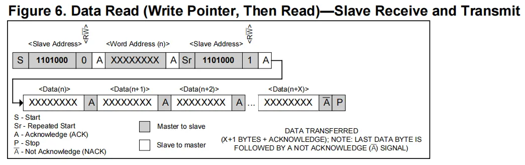
DS1307 operates as an I2C slave device, where the master device is responsible for generating the clock and START / STOP signals, and supports three I2C communication modes:
- Write Mode (Slave Reception): The master device first sends
DS1307the slave address (1101000 + write bit 0) and the target register address, then transmits data;DS1307responds byte by byte, with the register pointer automatically incrementing; - Read mode (slave transmission): The master device first sends the slave address (1101000 + read bit 1),
DS1307sends data after acknowledging, and the master device returns a non-acknowledgment to the last byte; - Write the pointer first then read: The master sends
START, slave address (write), register address, then sends a repeatedSTART, slave address (read),DS1307sends the data at the corresponding address, and the master finally returns a NACK to terminate the transmission.
2.8 PCB Routing Precautions
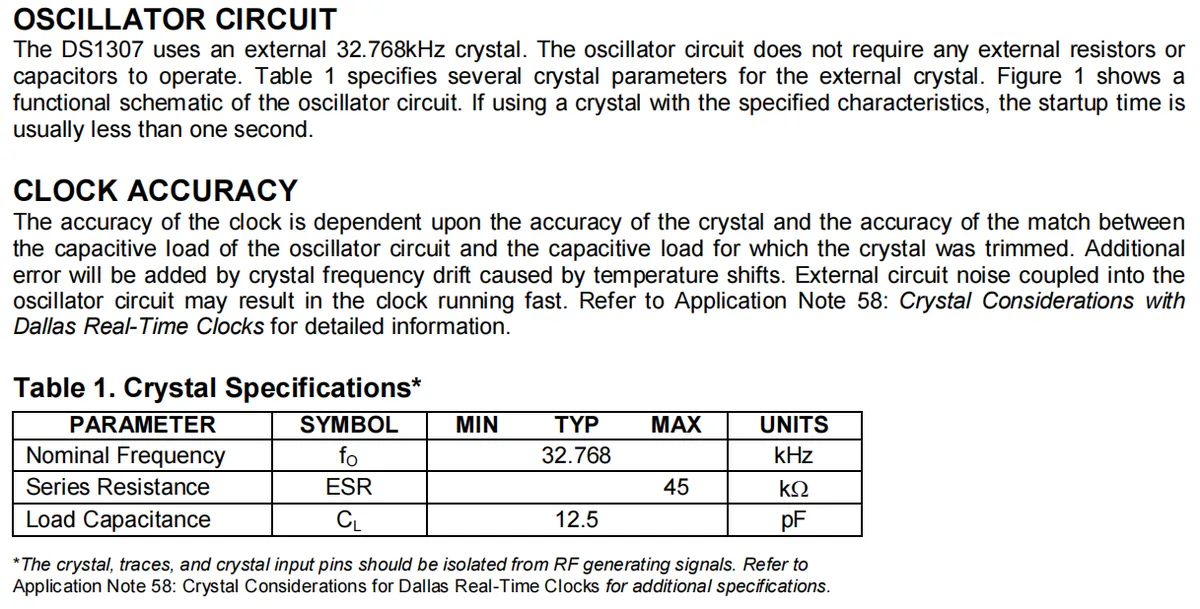
DS1307 requires an external 32.768kHz crystal oscillator for operation, with no external resistors or capacitors needed; the parameter requirements for the crystal oscillator are as follows: nominal frequency of 32.768kHz, maximum series resistance of 45kΩ, typical load capacitance of 12.5pF. Additionally, the crystal oscillator, corresponding traces and input pins must be kept away from RF signals, and the startup time of a crystal oscillator that meets the specifications is typically less than 1 second.
In addition, clock accuracy is related to the accuracy of the crystal oscillator, the capacitive load of the oscillator circuit, and the matching degree with the crystal oscillator. The frequency drift of the crystal oscillator caused by temperature changes and the external noise coupled into the oscillator circuit will increase the clock error and make the clock run fast respectively.
Recommended Layout for Crystal Oscillator
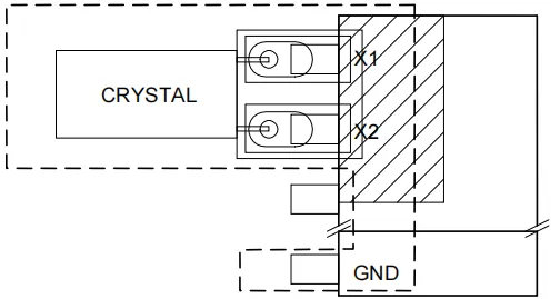
Note: Avoid routing signal traces in the cross-hatched area (upper left quadrant) of the package unless there is a ground plane between the signal traces and the device package.
III. Circuit Engineering
3.1 Circuit Source Engineering
To obtain the source project of the circuit, please follow the official account [Freak Embedded]
3.2 Module Usage Instructions
SCH_Schematic-DS1307 Chip-Based RTC Real-Time Clock Module-V1.1.0_2025-11-14.pdf 2.0 MB
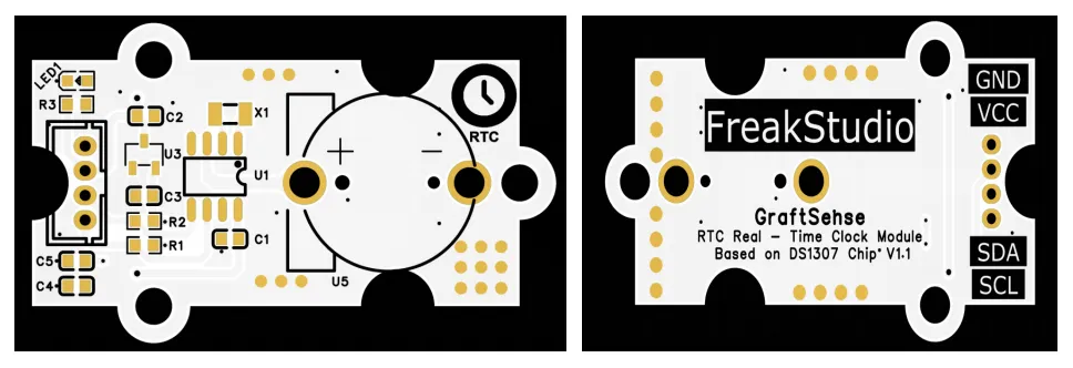
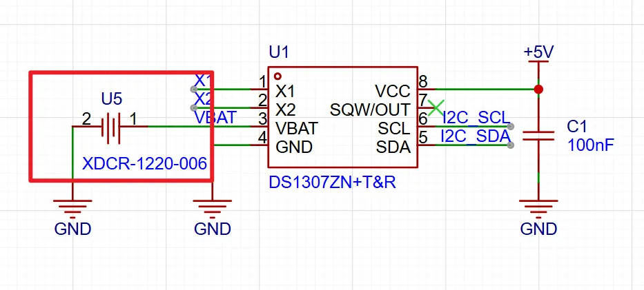
This module provides an I2C communication interface: it supports standard I2C communication rates, adopts a fixed I2C device address 0x68, is compatible with 3.3V/5V logic levels, can stably implement reading and writing of clock/calendar data (seconds, minutes, hours, dates, months, etc.) as well as data access of 56-byte RAM. It is applicable to scenarios such as time recording for maker projects, timing modules for embedded devices, and time synchronization for industrial instruments, providing the system with accurate real-time clock data interaction capabilities.
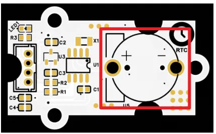
This module reserves a lithium battery holder for ensuring that DS1307ZN+ T&R can still keep time normally after power failure. If a 48 mAh lithium battery is used, DS1307ZN+ T&R can operate for ten years at 25°C (according to the datasheet).
3.3 Application Experiment
Here, we use the GraftPort-RP2040 development board for testing, and the RTC real-time clock module based on the DS1307 chip uses the I2C interface to communicate with the main controller.
Here, we first use the HY2.0-4P connection cable to connect the module to the GraftPort-RP2040 development board's I2C0 interface:
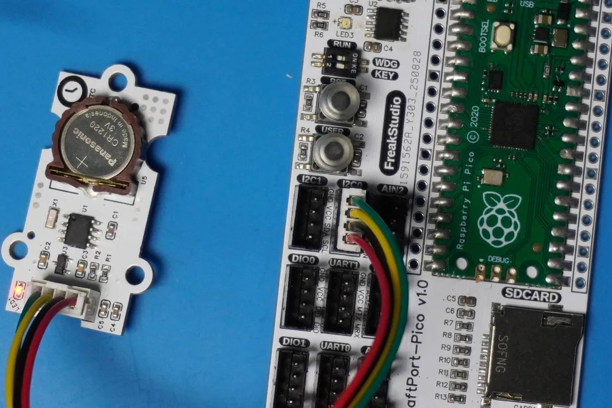
The module connections are shown in the following table
Development Board Pins | Module Pins | Description |
Pin 4 |
|
|
Pin 5 |
|
|
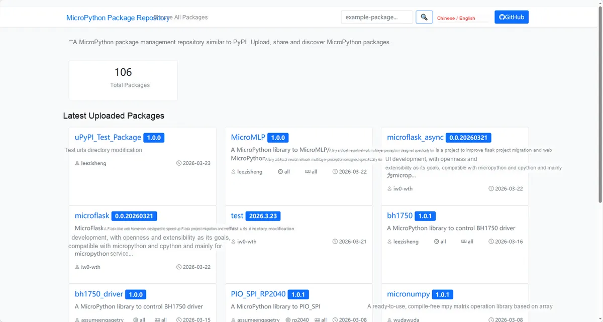
Here, we need to search for the relevant driver packages on uPyPI: https://upypi.net/zh/
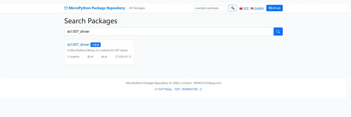
Enter ds1307_driver to search, and the following will be displayed:
Click to copy the local installation command:
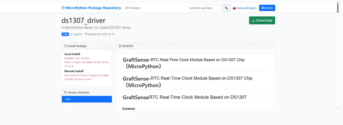
Here, we can use the mip tool to import module driver library code. Below are the usage commands for the mpremote tool:
mpremote mip install github:FreakStudioCN/GraftSense-Drivers-MicroPython/misc/DS1307_driverImport the RTC real-time clock module based on DS1307 chip - MicroPython driver code, then copy the following main.py code into our project:
# Python env   : MicroPython v1.23.0
# -*- coding: utf-8 -*-
# @Time    : 2025/9/8 4:52 PM
# @Author  : 缪贵成
# @File    : main.py
# @Description : RTC test: set time, read time, set Pico RTC time

# ======================================== Import Modules =========================================

from machine import Pin, I2C, RTC
import ds1307
import time

# ======================================== Global Variables ============================================

DS1307_ADDRESS = None

# ======================================== Functions ============================================

# ======================================== Custom Classes ============================================

# ======================================== Initialization configuration ===========================================

time.sleep(3)
print("FreakStudio: test ds1307 RTC now")
i2c = I2C(0, scl=Pin(5), sda=Pin(4), freq=100000)
# Start scanning for devices on the I2C bus and return a list of slave addresses
devices_list:list[int]=i2c.scan()
print('START I2C SCANNER')
# If the devices list is empty, no device is connected to the I2C bus
if len(devices_list) == 0:
    # If not empty, print the slave device addresses
    print("No i2c device !")
else:
    # Iterate over the slave device address list
    print('i2c devices found:', len(devices_list))
for device in devices_list:
    # Check whether the device address is the DS1307 address
    if 0x60 <= device <= 0x70:
        # Assume the first device found is at the DS1307 address
        print("I2c hexadecimal address:", hex(device))
        DS1307_ADDRESS = device

ds1307rtc = ds1307.DS1307(i2c, DS1307_ADDRESS)
print("DS1307 attributes:", dir(ds1307rtc))

# ========================================  Main Program  ============================================


# Oscillator switch test
ds1307rtc.disable_oscillator = True
print("disable_oscillator =", ds1307rtc.disable_oscillator)

ds1307rtc.disable_oscillator = False
print("disable_oscillator =", ds1307rtc.disable_oscillator, "\n")

# Read the current time
print("Current DS1307 datetime:", ds1307rtc.datetime, "\n")

# Set the time
# Parameters: (year, month, day, hour, minute, second, weekday, None)
ds1307rtc.datetime = (2025, 9, 17, 17, 47, 17, 6)

# Read the time again
print("After setting datetime:", ds1307rtc.datetime)

# Wait 3.9 seconds before reading
time.sleep(3.9)
print("After 3.9s:", ds1307rtc.datetime, "\n")

# Get the time in Pico RTC format
print("DS1307 datetime formatted for Pico RTC:", ds1307rtc.datetimeRTC, "\n")

# Print the Pico internal RTC time
print("Pico internal RTC time:", time.localtime(), "\n")

# Set the Pico RTC
rtc = RTC()
rtc.datetime(ds1307rtc.datetimeRTC)
print("Pico RTC set from DS1307, now:", time.localtime())
Burn the code, open a terminal, and use the mpremote tool to connect to the main controller; the output is as follows:
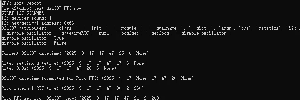
It can be seen that we can normally read the time-related data.
IV. Drivers
DS1307_driver.zip 12 KB
5. BOM & Recommended Alternative Parts
None.
VI. Revision History
Document Version | Date of Revision | Modifier | Modified Content |
v1.0 | 2025-11-14 | Ling Gaoxing | Initialize the document |
v1.1 | 2025-12-29 | Li Zisheng | Added application experiments and production files |
v1.2 | 2025-12-31 | Xin Ruili | Create an open version of the document based on the internal document version v1.1. |
v1.3 | 2026-03-29 | Xin Ruili | Modified the application experiment section |