Contents
- I. Module Introduction
- II. Introduction to Major Chips
- 2.1 Chip Overview
- 2.2 Pin Definition
- 2.3 Functional Block Diagram
- 2.4 Performance Parameters
- 2.5 Reference Circuit
- 2.6 Chip Configuration
- 2.7 Communication Interfaces and Related Protocols
- 2.8 PCB Routing Precautions
- III. Instructions for Circuit Engineering and Module Usage
- 3.1 Circuit Source Engineering
- 3.2 Module Usage Instructions
- 3.3 Application Experiment
- IV. Drivers
- 5. BOM & Recommended Alternative Parts
- VI. Revision History
- VII. Relevant Materials
- 7.1 Chip Datasheet
- 7.2 Unique Icons for PCB Silkscreen
I. Module Introduction
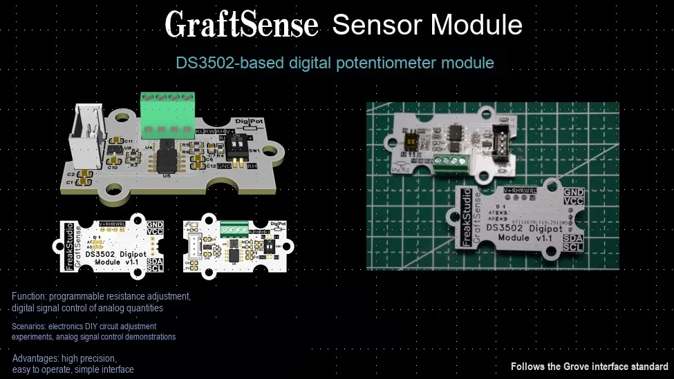
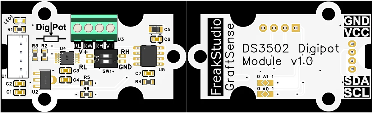
DS3502-based digital potentiometer module supports I2C communication (SDA, SCL interfaces), is equipped with address setting DIP switches (A0, A1), and enables digital potentiometer adjustment via the I2C protocol; it integrates step-down voltage regulation, power filtering and indicator lights, is suitable for scenarios such as maker development and circuit debugging, requires the input signal frequency to be less than 400KHz, and provides a programmable resistance adjustment solution for the system.
II. Introduction to Major Chips
2.1 Chip Overview
The DS3502 is a 7-digit digital potentiometer, which can be communicated with via the I2C interface using a microcontroller to adjust its resistance value. The DS3502 provides 128 resistance adjustment steps, and this device supports a wide range of supply voltages, typically operating between 2.7V and 5.5V.
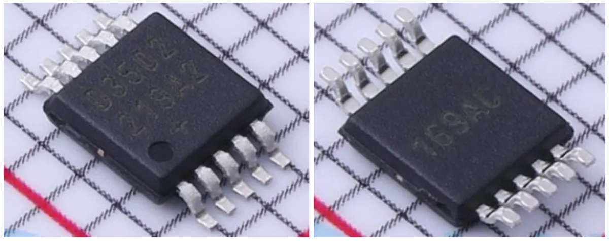
DS3502 can operate at speeds up to 400kHz, with a maximum resistance value of 10kΩ. By adjusting the two address setting pins, it supports up to four DS3502 digital potentiometers on the same bus, and it also has EEPROM function, which can save the set 7-bit resistance value after power failure.
2.2 Pin Definition
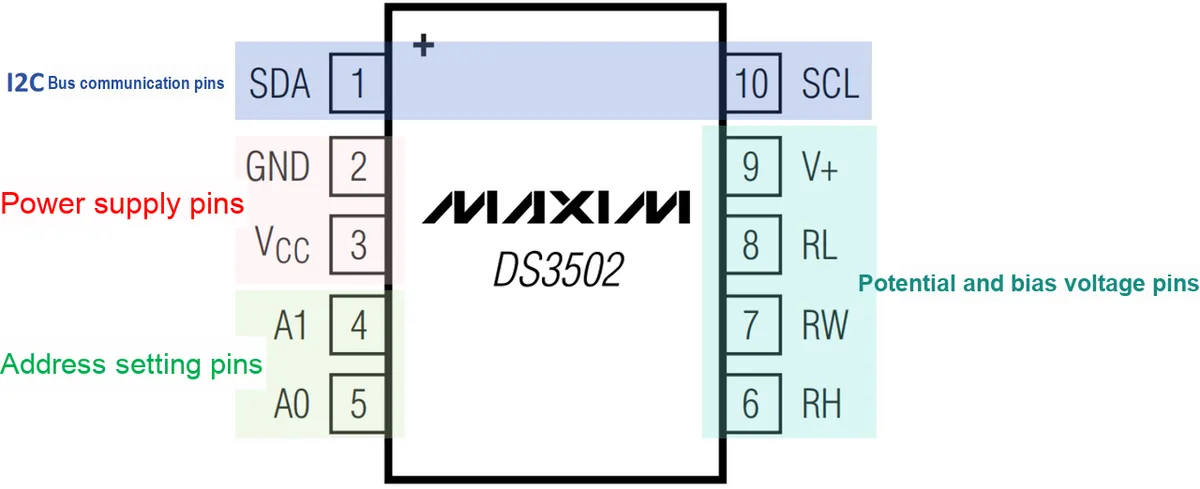
DS3502 The pins and their functions are as follows:
Pin Name | Pin Number | Pin Functions |
SDA | 1 | I2C Serial Data: Used for the input and output of I2C data. The voltage of SDA ranges from -0.5V to (VCC + 0.5V), and shall not exceed + 6.0V. |
SCL | 10 | I2C Serial Clock: The input pin of the I2C clock, which is responsible for synchronizing data transmission. The voltage of SCL ranges from -0.5V to (VCC + 0.5V), and shall not exceed + 6.0V. |
VCC | 3 | Power supply voltage terminal: Connect to an external power source to provide the operating voltage required for the device, which is typically in the range of 2.5V to 5.5V. |
GND | 2 | Ground terminal: the grounding terminal of a device, which serves as the reference point for the circuit. |
A1, A0 | 4, 5 | Address selection input: Used to specify the I2C slave device address. |
RH | 6 | High-end terminal: the high end of a potentiometer, connected to the positive power supply in the application. The voltage range is from -0.5V to V+. |
RW | 7 | Slider terminal: The sliding end of a potentiometer, which outputs an adjustable voltage and is usually connected to a load or a subsequent circuit. The voltage range is from -0.5V to V+. |
RL | 8 | Low-end terminal: the low end of a potentiometer, connected to ground or a negative power supply. The voltage range is from -0.5V to V+. |
V+ | 9 | Slide bias voltage: It provides a bias voltage for the sliding terminal, with a voltage range from -0.5V to + 17V, which affects the output voltage range. |
2.3 Functional Block Diagram
DS3502 The internal structure of the chip is shown below, and its core units include I2C communication interface, control register, tap register and resistor network:
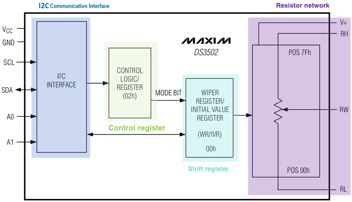
The sliding position of the DS3502 is controlled by the value in the Wiper Register (WR). Upon power-up, the initial value of the sliding position is programmed via the Initial Value Register (IVR); after power-up, the data in the IVR register is loaded into the WR register, thereby setting the initial position of the potentiometer's wiper terminal (RW).

The Control Register (Control Register, CR) is located at address 02h and contains the WR / IVR address mode bit (MODE bit); the MODE bit determines how to write to the I2C WR and IVR data registers:
MODE= 0 : WhenI2Cwrites address 00h, the data is written toWRandIVR(CR= 00h); whenI2Creads from address00h, returns the content ofWR, this mode is slow because it involvesEEPROMregister writing.MODE= 1:When the I2Cwrites to address 00h, onlyWR(CR= 80h) is written;when the I2Creads from address 00h, the content ofWRis still returned. This mode allows fast writing toSRAMwithout waiting for the write delay of theEEPROMregister.
EEPROM and SRAM retain their data when the MODE bit is switched; upon power-up, the default value of the CR control register is 00h.
DS3502 potentiometer consists of 127 series-connected resistors connected between the RH and RL pins. By changing the value (a decimal value ranging from 0 to 127) in the wiper register (Wiper Register, WR), DS3502 's internal decoder controls specific MOS transistors to turn on or off. The MOS transistors act as switches in the resistor network to select which resistor node the wiper terminal (RW) is connected to:
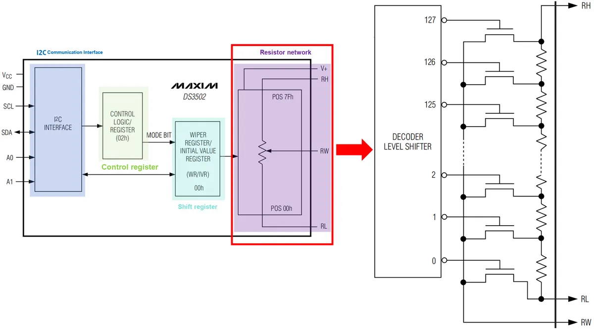
MOStransistor turn-on: When a control signal turns on a certainMOStransistor, the resistor segment corresponding to thisMOStransistor is incorporated into the circuit;MOSturn-off: WhenMOSis turned off, the corresponding node is disconnected from the sliding terminalRW, so that no current can flow through this path, andRWis independent of this resistor segment.
Based on this principle, we can adjust DS3502 the resistance of the potentiometer's wiper terminal to achieve different voltage outputs. If RH, RL and RW are connected in a voltage divider configuration, the voltage across RW can be calculated using the following formula:
Wherein,is the wiper position, expressed in decimal (0-127),is the voltage at the RL terminal,and is the voltage at the RH terminal.
Here, in the electrical characteristics section of the DS3502 chip datasheet, we can see that after the wiper is adjusted to a new resistance value, it takes 1μs (i. e., the Wiper response time tWRS) to stabilize:
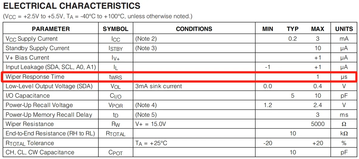
Therefore, theoretically, when the DS3502 acts as a variable voltage divider to adjust the output voltage, its maximum operating frequency is 1 MHz (1/tWRS).
2.4 Performance Parameters
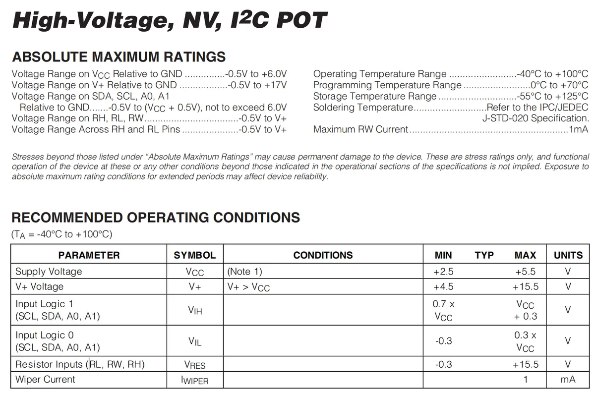
- Absolute Maximum Ratings
- Power supply voltage (
VCCrelative toGND): -0.5V ~ + 6.0V; V+relative toGNDvoltage range: -0.5V ~ + 17V;SDA,SCL,A0,A1relative toGNDvoltage range: -0.5V ~(VCC+ 0.5V)(not exceeding 6.0V);RH,RW,RLpin voltage range relative toGND: -0.5V toV+;RHandRLpin voltage range: -0.5V ~ V+;- Operating temperature range: -40℃ ~ + 100℃;
- Maximum
RWCurrent: 1mA.
- Power supply voltage (
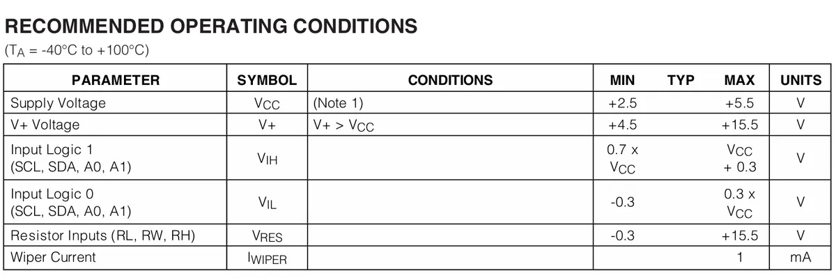
- Recommended Operating Conditions
- Supply Voltage (
Vcc): 2.5V ~ 5.5V; V+voltage (V+>Vcc): 4.5V ~ 15.5V;- Input logic 1 voltage (
SCL,SDA,A0,A1): 0.7 ×VCC~VCC+ 0.3V; - Input logic low voltage (
SCL,SDA,A0,A1): -0.3V ~0.3×Vcc; - Voltage of resistor input (
RL,RW,RH): -0.3V ~ + 15.5V; - Wiper current (
I_WIPER): max. 1 mA.
- Supply Voltage (
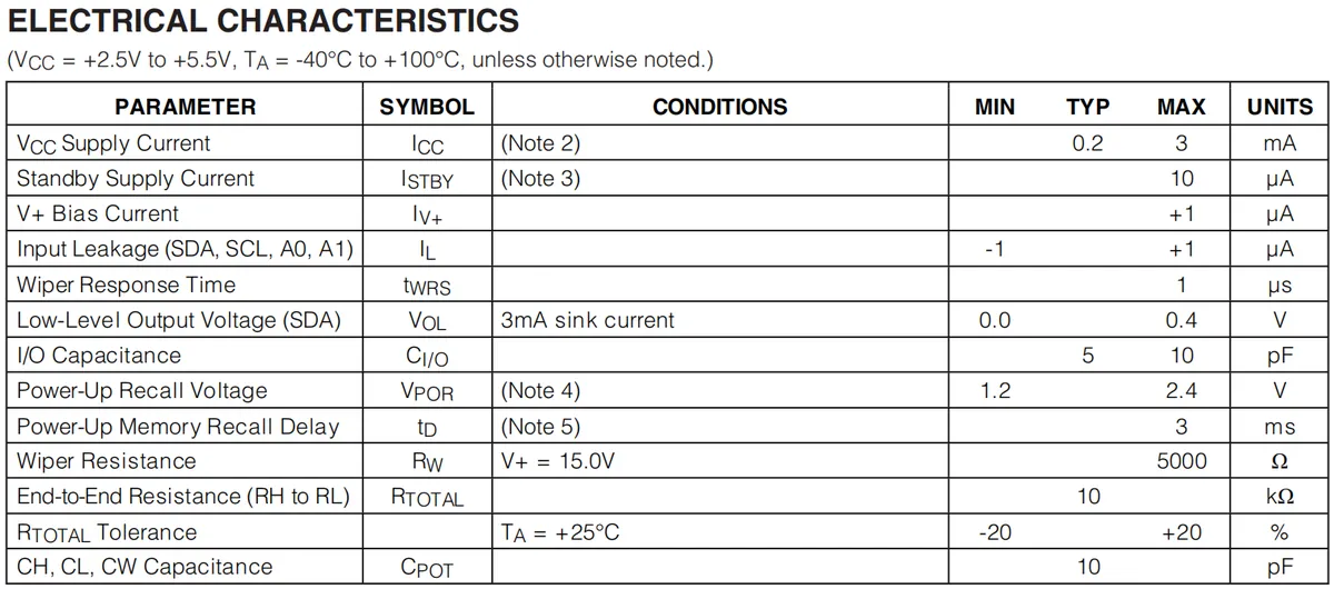
VccSupply Current (I₍CC₎): Refer to Note 2 for test conditions, typical value is 0.2mA, maximum value is 3mA, unit: mA;- Standby supply current (
I₍STBY₎): See Note 3 for conditions, maximum 10 μA; V+Bias Current (I₍V+₎): Max. + 1μA;- Input leakage current (
SDA,SCL,A0,A1)(I₍L₎): Range -1 to + 1 μA; - Slider response time (
t₍WRS₎): max. 1 μs; SDALow-level output voltage (V₍OL₎): 0.0~0.4V at a sink current of 3mA;I/OCapacitance (C₍I/O₎): Typical 5 pF, maximum 10 pF;- Power-on reset voltage (
V₍POR₎): 1.2~2.4V; - Power-on memory access delay (
t₍D₎): max. 3ms; - Slide rheostat (
R₍W₎):When V+= 15.0 V, the maximum resistance is 5000 Ω. - End-to-end resistance (
RHtoRL)(R₍TOTAL₎): typical 10 kΩ; R₍TOTAL₎Tolerance:TA= -20~+ 20% at + 25℃;CH,CL,CWcapacitance (C₍POT₎): typical 10 pF.
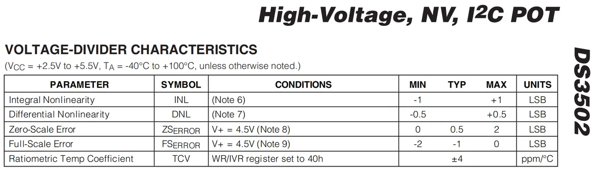
- Integral Nonlinearity (
INL): Refer toNote 6for conditions, ranging from -1 to + 1LSB; - Differential Non-Linearity (
DNL): Conditions refer toNote7, ranging from -0.5 to + 0.5LSB; - Zero-scale error (
ZSError): V+= 4.5V (Note8), 0~2LSB, typical value 0.5LSB; - Full-scale error (
FSError): V+= 4.5V (Note 9), -2 to 0LSB, typical -1LSB; - Ratio Temperature Coefficient (
TCV):WR/IVRregister is set to 40h, typically ±4 ppm/℃.
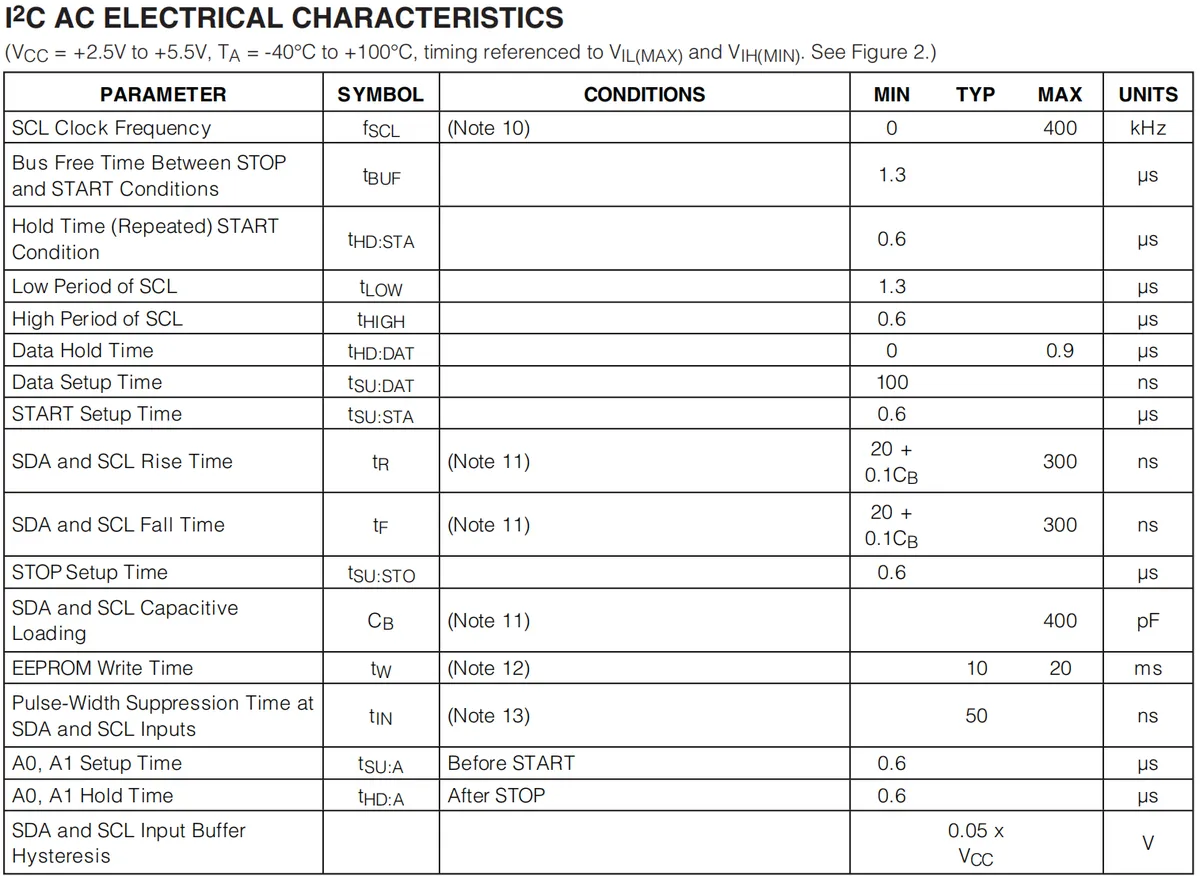
SCLclock frequency (f₍SCL₎): Refer toNote 10for conditions, max. 400 kHz;- The bus between
STOPandSTARTconditions (t₍BUF₎): minimum 1.3 μs; - Repeated
STARTcondition hold time (t₍HD: STA₎): minimum 0.6 μs; SCLLow Period (t₍LOW₎): Minimum 1.3 μs;SCLhigh period (t₍HIGH₎): minimum 0.6 μs;- Data Hold Time (
t₍HD: DAT₎): Typical value 0.9 μs; - Data setup time (
t₍SU: DAT₎): minimum 100 ns; STARTSetup Time (t₍SU: STA₎): Min. 0.6 μs;SDAandSCLrise time (t₍R₎): Refer toNote 11for conditions, formula20 + 0.1C₍B₎, maximum 300 ns;SDAandSCLfall time (t₍F₎): Refer toNote 11for conditions, formula:20 + 0.1C₍B₎, maximum 300 ns;STOPSetup Time (t₍SU: STO₎): Min. 0.6 μs;SDAandSCLcapacitive load (C₍B₎): Refer toNote 11, maximum 400 pF;EEPROMwrite time (t₍W₎): Refer toNote 12for conditions, typical value 10 ms, maximum 20 ms;SDAandSCLinput pulse width suppression time (t₍IN₎): Conditions refer to Note 13, typical value 50 ns;A0,A1Setup Time (t₍SU: A₎):Before START, minimum 0.6 μs;A0,A1Hold Time (t₍HD: A₎):After STOP, minimum 0.6 μs;SDAandSCLinput buffer hysteresis: typical0.05×Vcc.
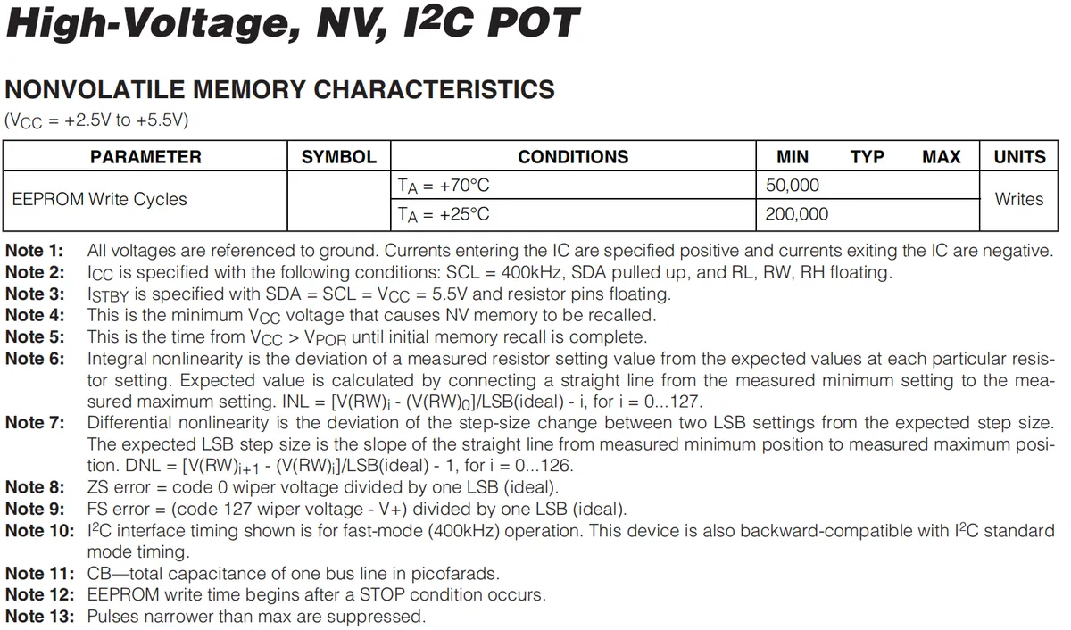
EEPROMWrite Cycle:TA= + 70℃, minimum 50,000 write cycles;TA= + 25℃, minimum 200,000 write cycles
2.5 Reference Circuit
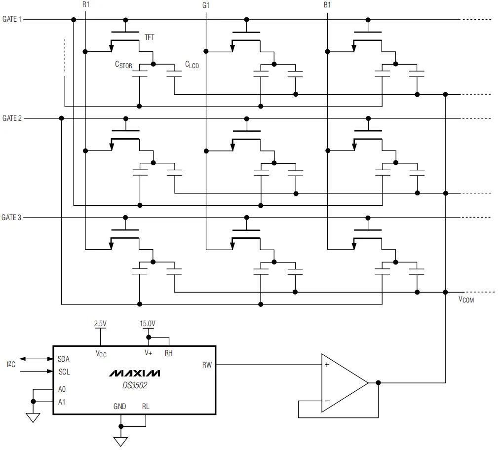
2.6 Chip Configuration
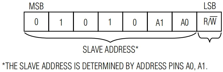
DS3502 chip's I2C communication address is determined by the two pins A1 and A0:
2.7 Communication Interfaces and Related Protocols
When writing single-byte data to the DS3502 chip using a microcontroller, it is necessary to write the device address (pins A0 and AI in the figure below are both connected to GND), the register address and the write data, as shown below:

For example, when writing to the WR register, the communication process is as follows:

When the CR register MODE bit is set to 0, since writing to the EEPROM register requires a certain period of time, the master device can repeatedly address the DS3502 to check whether it responds, so as to determine whether the DS3502 has completed writing to the EEPROM register; alternatively, the master can directly wait for the maximum EEPROM write time (tW), which can be found in the electrical characteristics section of the DS3502 datasheet and is specified as 20ms:

When using a microcontroller to read single-byte data from the DS3502 chip, take reading the value of the CR control register as an example:
- First, send the slave address byte and set the
R/Wbit to 0 to perform a dummy write operation, then the slave will send anACKresponse signal; - Write the memory address to be read
02h, and the slave sends anACKresponse signal; - Generate duplicate
STARTconditions to maintain communication; - Write the slave address again and set
the R/Wbit to 1, indicating that data is to be read; - The slave device sends a single-byte data of the corresponding register, the master device reads the data byte, uses the
NACKsignal to indicate the end of transmission, and generates aSTOPcondition.
When using the DS3502 chip, note that decoupling capacitors of 0.01µF and 0.1µF should be used for the power supply pin (VCC) and the sliding voltage pin (V+), and 4.7kΩ pull-up resistors should be applied to the SDA and SCL pins;additionally, if the voltage of RH is higher than that of VCC, V+ must be kept at the same or a higher voltage level as RH, which means V+ should be connected to RH.
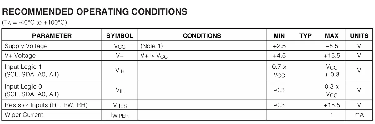
Meanwhile, it should be noted that the voltage range of the sliding voltage pin (V+) is + 4.5V to 15.5V:
2.8 PCB Routing Precautions
None.
III. Instructions for Circuit Engineering and Module Usage
3.1 Circuit Source Engineering
To obtain the source project of the circuit, please follow the official account [Freak Embedded]
3.2 Module Usage Instructions
The schematic diagram of this module is shown below:
SCH_Digital Potentiometer Module Based on DS3502_v1.0_2025-11-23.pdf 1.8 MB
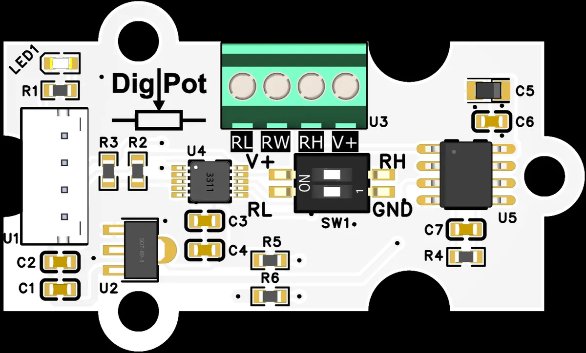
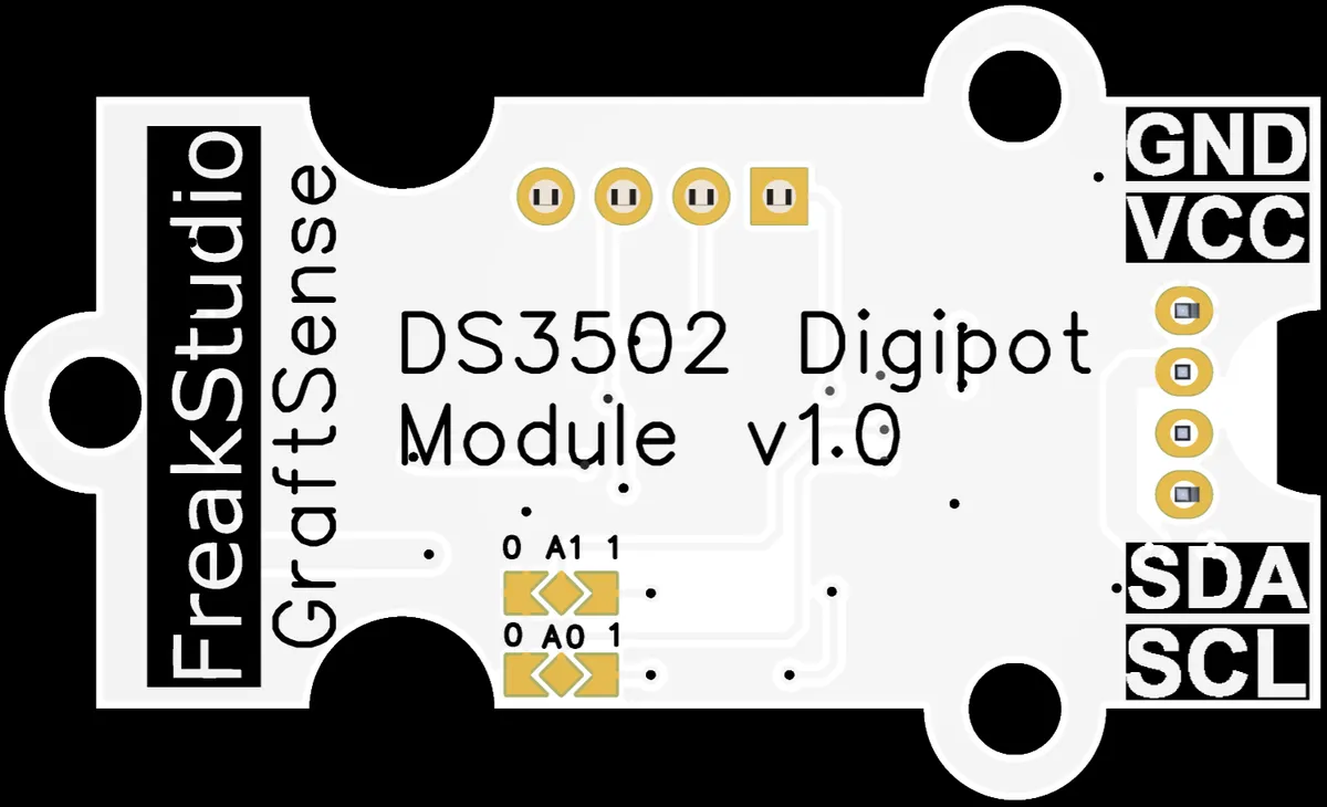
This module provides an I2C interface for communication: it supports a maximum I2C clock frequency of 400kHz, is compatible with I2C standard mode and fast mode, and can realize programmable adjustment of the digital potentiometer through this interface. Meanwhile, with the help of the I2C communication mechanism, it can also realize non-volatile storage of potentiometer settings, ensuring that parameters are permanently retained after power-off, which is suitable for scenarios requiring dynamic and stable resistance adjustment such as circuit debugging and signal conditioning.
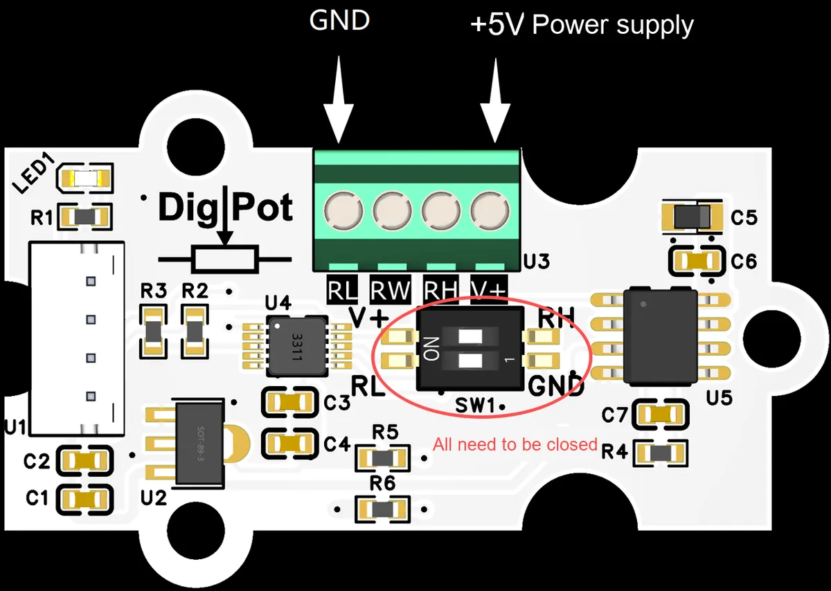
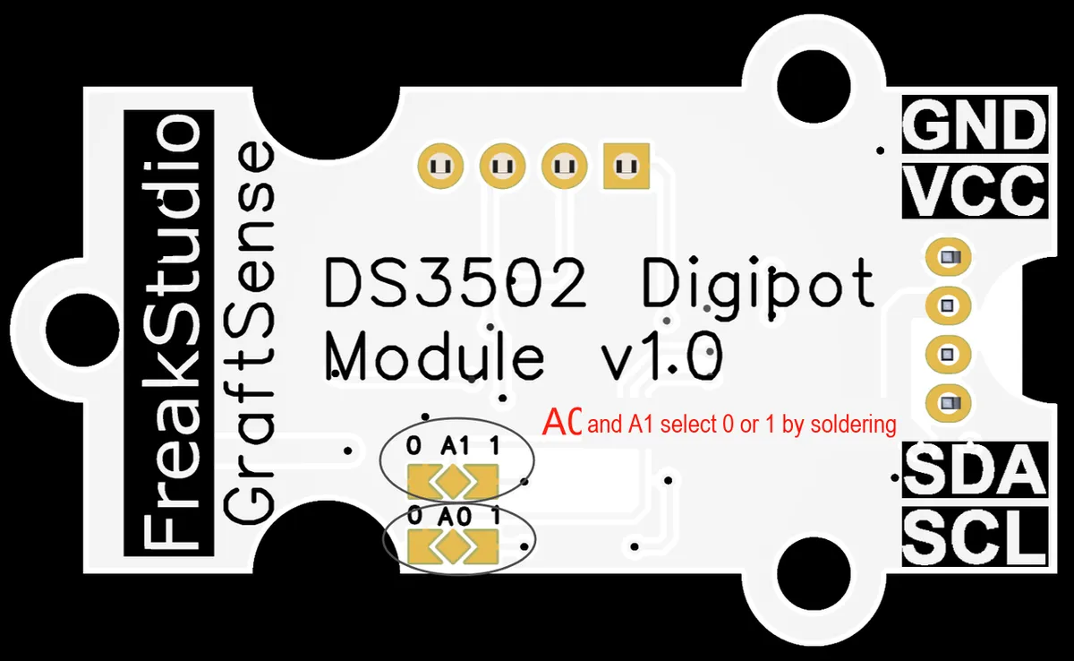
When using this module, you need to short the three sets of pads of the address selection pins A0 and A1 on the back of the module to GND or VCC to configure the device address; in addition, turn on the SW1 DIP switch's RL to short it to GND, turn on its V+ to short it to RH, and connect a power supply (e. g. + 5V) to the U3 terminal's RL and V+ pins:
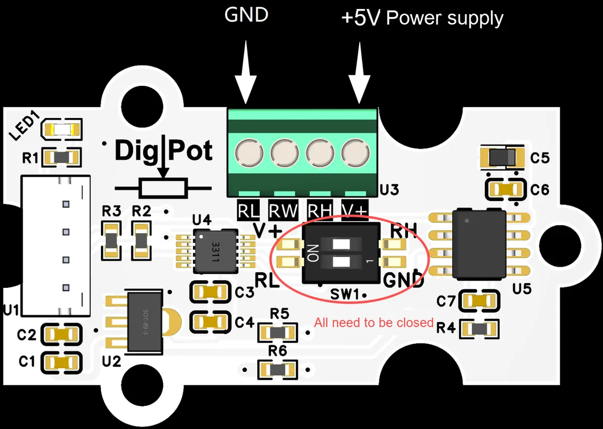
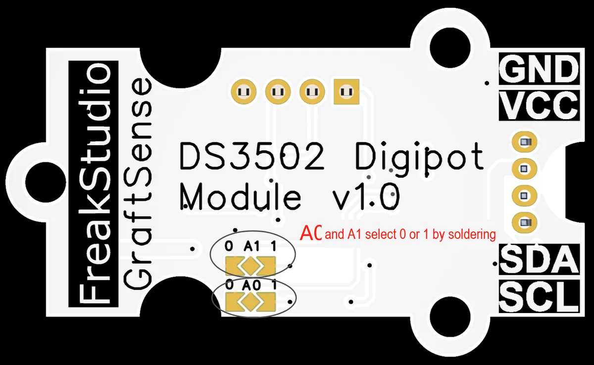
Note that if the voltage at RH is higher than VCC, V+ must be maintained at the same or a higher voltage level as RH; that is, V+ shall be connected to RH.
Meanwhile, it should be noted that the voltage range of the sliding voltage pin (V+) is + 4.5V to 15.5V:
3.3 Application Experiment
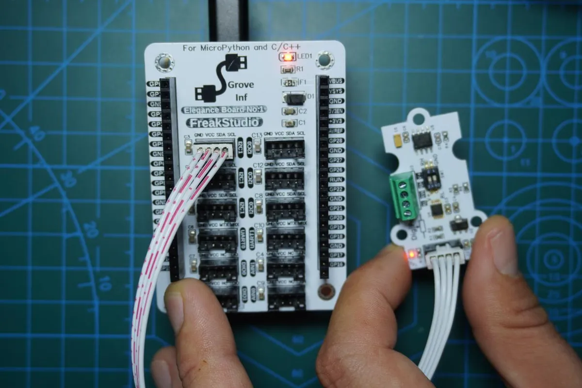
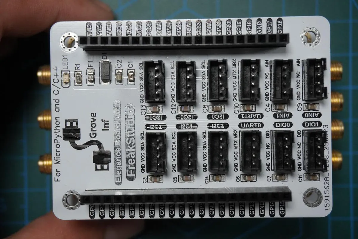
Here, we use the Fengya No. 1 board for testing. First, you need to plug the Fengya No. 1 Board - Grove Interface Expansion Board into the Fengya No. 1 Board - Universal Compatible Expansion Board, and meanwhile use a 4P cable to connect the I2C1 port on the Fengya No. 1 Board - Grove Interface Expansion Board with the I2C port on the GraftSense - DS3502-based Digital Potentiometer Module:
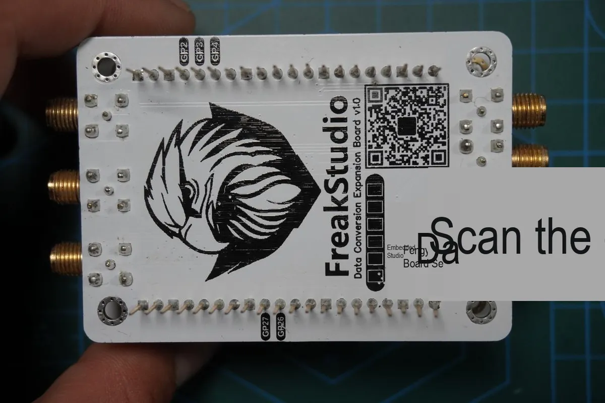
Then insert the Fengya No.1 Board-Universal Compatible Expansion Board into the Fengya No.1 Board-Data Conversion Board , and open the SCL , SDA and RDY options of the Fengya No.1 Board-Data Conversion Board on the SWITCH1 DIP switch, and open the ADC1 switch option of the SWITCH2 DIP switch:
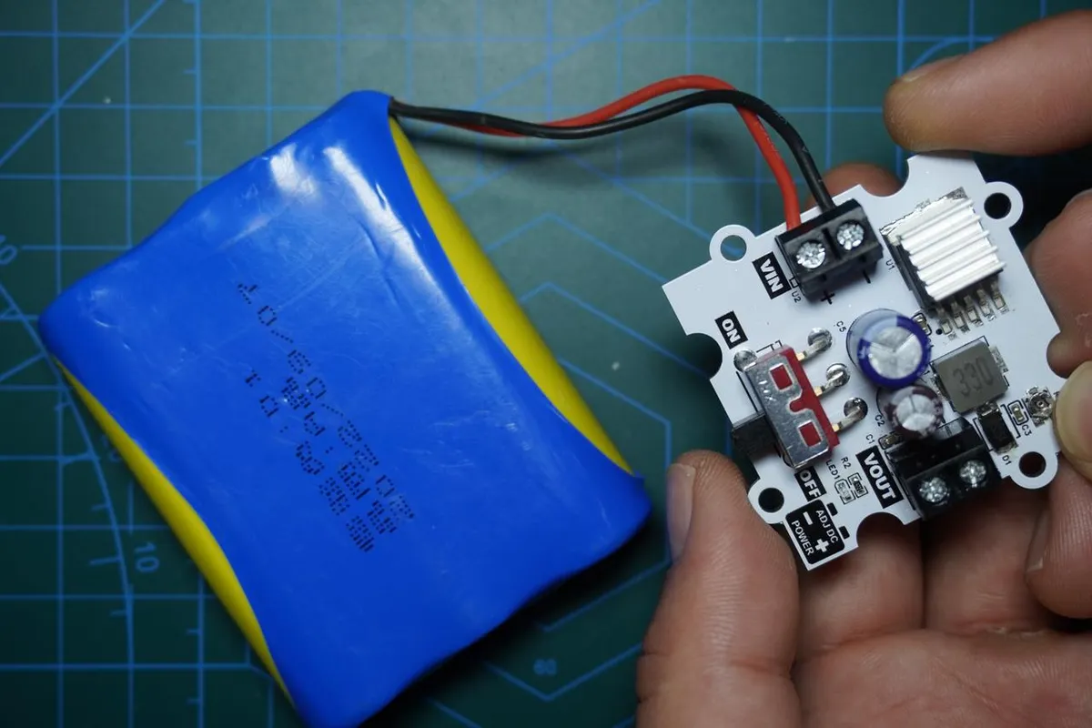
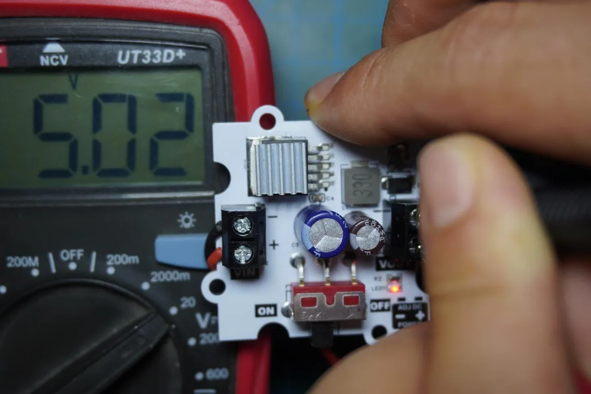
Before conducting application experiments, you need to on the back side of the DS3502-based digital potentiometer module configure the device address by shorting the three pads of the address selection terminals A0 and A1 to GND or VCC; in addition, turn on the RL of the DIP switch SW1 to short it with GND, turn on the V+ to short it with RH, and connect a + 5V power supply to the RL and V+ on the U3 terminal (it is recommended to use the GraftSense - LM2596S-based adjustable power supply module):
The physical image after insertion is as follows:
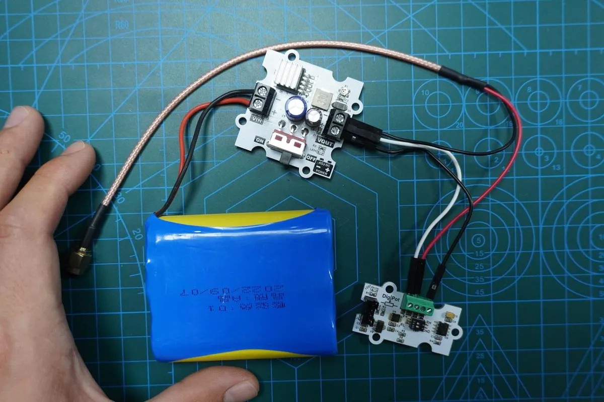
Here, the signal output interface on the DS3502-based digital potentiometer module is the terminal U3 's RW. We also need to use an SMA to DuPont wire adapter to connect the RW signal output interface of terminal U3 on the GraftSense - DS3502-based digital potentiometer module to the ADC0 internal analog-to-digital conversion SMA interface on the Fengya No. 1 Board - Data Conversion Board , as shown in the following figure:
In addition, we first need to connect the MiniUSB data cable to the serial port on the Fengya No. 1 Board - Universal Compatible Expansion Board; here, GP0 and GP1 are the default pins of the Raspberry Pi Pico's hardware serial port UART0:
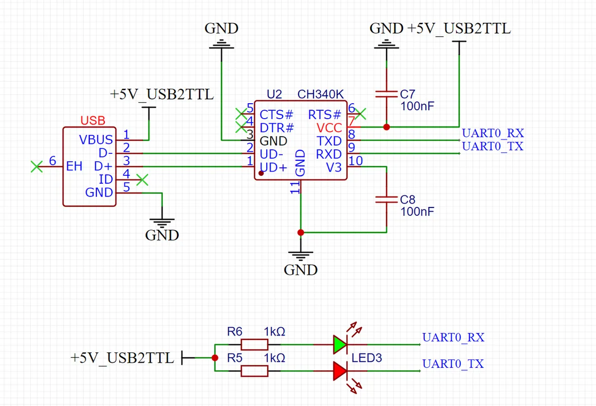
Here, the digital potentiometer module based on DS3502 on the signal output interface is the RW of terminal U3 , we also need to use SMA to DuPont cable adapter to digital potentiometer module based on DS3502 on the terminal U3 of the RW signal output interface and Fengya No.1 board - data conversion board on the ADC0 internal analog-to-digital conversion SMA interface are connected to each other, as shown in the following figure:
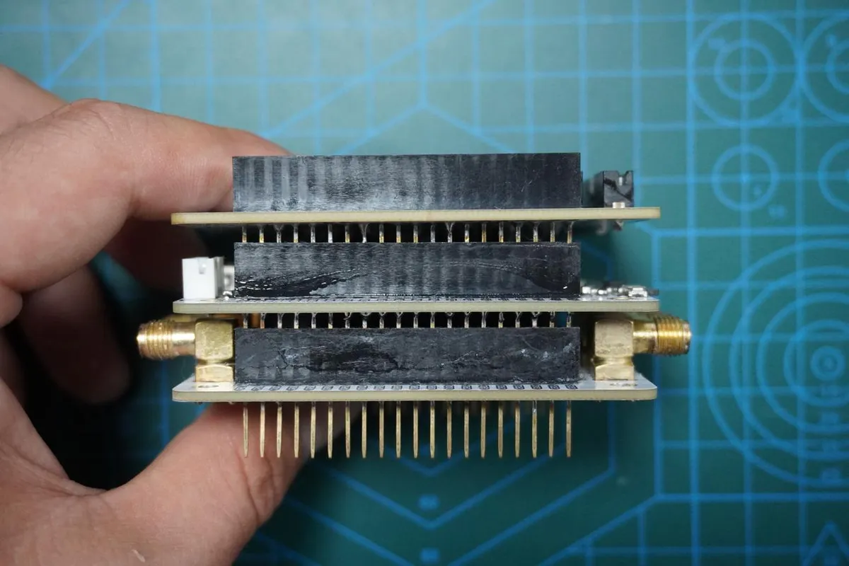
The overall connection diagram is shown as follows:
The wiring conditions of the components are shown in the following table:
| Module / Device | Pin / Interface / Configuration item | Connection target | Target pin / Interface |
| Raspberry Pi Pico (core of the Fengya No. 1 board) | GP10 (I2C1_SDA) | Grove interface expansion board I2C1 | SDA pin |
| Raspberry Pi Pico (core of the Fengya No. 1 board) | GP11 (I2C1_SCL) | Grove interface expansion board I2C1 | SCL pin |
| Grove interface expansion board | I2C1_SDA | DS3502 module I2C | SDA interface |
| Grove interface expansion board | I2C1_SCL | DS3502 module I2C | SCL interface |
| DS3502 module | Address select pin A0 | GND/VCC | Pad shorted |
| DS3502 module | Address select pin A1 | GND/VCC | Pad shorted |
| DS3502 module | SW1 DIP switch RL | Module internal GND | DIP switch shorted |
| DS3502 module | SW1 DIP switch V+ | Module internal RH | DIP switch shorted |
| 3.3V power supply | Output terminal | DS3502 module U3 terminal | RL interface |
| 3.3V power supply | Output terminal | DS3502 module U3 terminal | V+ interface |
| Raspberry Pi Pico (core of the Fengya No. 1 board) | GP0 (UART0_TX) | Universal compatible expansion board serial port | TX pin |
| Raspberry Pi Pico (core of the Fengya No. 1 board) | GP1 (UART0_RX) | Universal compatible expansion board serial port | RX pin |
| Universal compatible expansion board | Serial port interface | MiniUSB cable | USB male end |
| DS3502 module | U3 terminal RW (signal output) | Data conversion board ADC0 | SMA interface |
| Data conversion board | ADC0 interface | Raspberry Pi Pico (core of the Fengya No. 1 board) | GP26 (ADC0) |
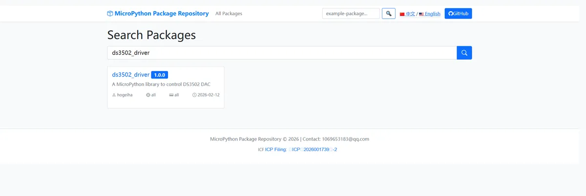
Here, we need to search for the relevant driver packages on uPyPI: https://upypi.net/zh/
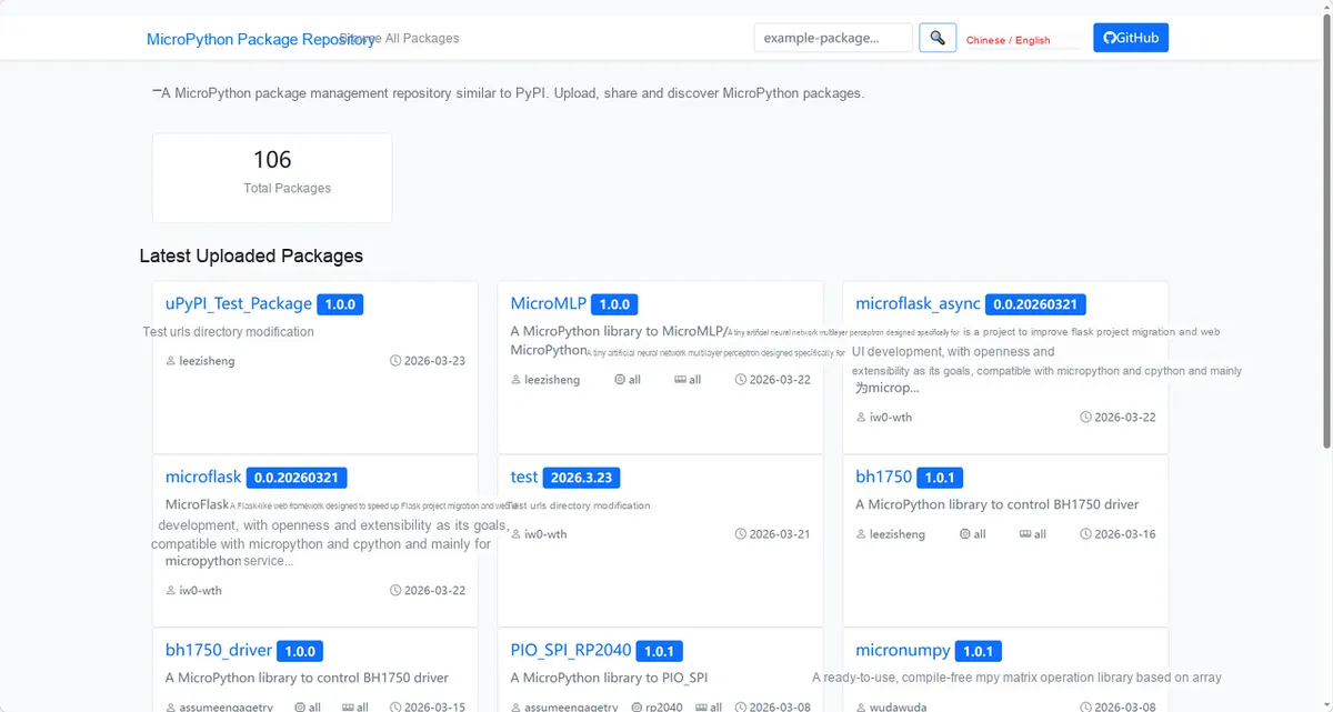
Enter ds3502_driver for search, and the following will be displayed:
Click to copy the local installation command:
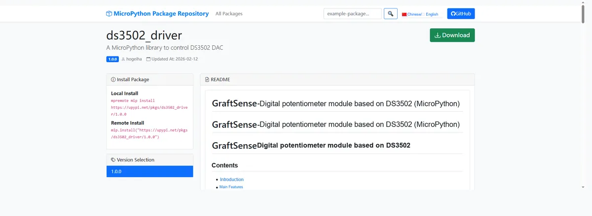
Here, we can use the mip tool to import module driver library code. Below are the usage commands for the mpremote tool:
mpremote mip install github:FreakStudioCN/GraftSense-Drivers-MicroPython/signal_generation/ds3502_driverAfter importing the digital potentiometer module based on DS3502 - MicroPython driver code, copy the following main.py code into our project:
# Python env   : MicroPython v1.23.0
# -*- coding: utf-8 -*-
# @Time    : 2025/3/21 3:04 PM
# @Author  : Li Qingshui
# @File    : main.py
# @Description : Output arbitrary waveforms using the DS3502 digital potentiometer

# ======================================== Import Modules ========================================

# Import the hardware module
from machine import ADC, Timer, Pin, I2C, UART
# Import time-related modules
import time
# Import the module for accessing and controlling MicroPython internals
import micropython
# Import the ds3502 module used to control the digital potentiometer chip
from ds3502 import DS3502
# Import the waveform generation module
from dac_waveformgenerator import WaveformGenerator

# ======================================== Global Variables ============================================

# DS3502 chip address
DAC_ADDRESS = 0x00
# Voltage conversion factor
adc_conversion_factor = 3.3 / (65535)

# ======================================== Functions ============================================

def timer_callback(timer: Timer) -> None:
    """
    Timer callback function, used to read ADC data periodically and call the user-defined callback function.

    Args:
        timer (machine.Timer): Timer instance.

    Returns:
        None: This function has no return value.

    Raises:
        None: This function does not raise exceptions.
    """

    # Declare global variables
    global adc, adc_conversion_factor

    # Read ADC data
    value = adc.read_u16() * adc_conversion_factor
    # Call the user-defined callback function
    micropython.schedule(user_callback, (value))

def user_callback(value: float) -> None:
    """
    User-defined callback function, used to process the voltage value sampled by the ADC and send it over the serial port.

    Args:
        value (float): Voltage value sampled by the ADC.

    Returns:
        None: This function has no return value.

    Raises:
        None: This function does not raise exceptions.
    """
    # Declare global variables
    global uart

    # Get the floating-point number and round it to two decimal places
    formatted_value = "{:.2f}".format(value)
    # Send the sampled voltage data over the serial port
    uart.write(str(formatted_value) + '\r\n')

# ======================================== Custom Classes ============================================

# ======================================== Initialization ==========================================

# Delay 3 s to wait for the device to finish powering up
time.sleep(3)
# Print debug information
print("FreakStudio : Using Digital Potentiometer chip DS3502 to generate differential waveform")

# Create a hardware I2C instance using the I2C1 peripheral, with a clock frequency of 400KHz, SDA pin 2, and SCL pin 3
i2c = I2C(id=1, sda=Pin(2), scl=Pin(3), freq=400000)

# Start scanning for devices on the I2C bus and return a list of slave addresses
devices_list = i2c.scan()
print('START I2C SCANNER')

# If devices_list is empty, no device is connected to the I2C bus
if len(devices_list) == 0:
    print("No i2c device !")
# If not empty, print the slave device addresses
else:
    print('i2c devices found:', len(devices_list))
    # Iterate over the slave device address list
    for device in devices_list:
        # If the device address is between 0x28 and 0x2B, it is a DS3502 chip
        if 0x28 <= device <= 0x2B:
            print("I2C hexadecimal address: ", hex(device))
            DAC_ADDRESS = device

# Create a DS3502 object using the I2C1 peripheral, with address DAC_ADDRESS
dac = DS3502(i2c, DAC_ADDRESS)
# Set the DS3502 to fast mode (write only to the WR register)
dac.set_mode(1)

# Create the serial port object, set the baud rate to 115200
uart = UART(0, 115200)
# Initialize the uart object with a baud rate of 115200, 8 data bits, no parity bit, and 1 stop bit
# Set the serial port timeout to 100ms
uart.init(baudrate=115200,
          bits=8,
          parity=None,
          stop=1,
          tx=0,
          rx=1,
          timeout=100)

# Create an ADC instance: ADC2-GP28
adc = ADC(2)
# Create a software timer object
timer = Timer(-1)
# Start the timer, triggering the timer_callback function every 1ms; the ADC samples the voltage
timer.init(period=10, mode=Timer.PERIODIC, callback=timer_callback)

# ========================================  Main Program  ===========================================

# Generate the sine wave
print("FreakStudio : Generate Sine Waveform : 10Hz, 1.5V, 1.5V")
# Initialize the waveform generator
wave = WaveformGenerator(dac, frequency=5, amplitude=1.5, offset=1.5, waveform='sine')
# Start waveform generation
wave.start()
# Stop generation after running for a while
time.sleep(6)
wave.stop()

# Generate square wave
print("FreakStudio : Generate Square Waveform : 10Hz, 1.5V, 1.5V")
# Initialize the waveform generator
wave = WaveformGenerator(dac, frequency=5, amplitude=1.5, offset=1.5, waveform='square')
# Start waveform generation
wave.start()
# Stop generation after running for a while
time.sleep(6)
wave.stop()

# Generate triangle wave
print("FreakStudio : Generate Triangle Waveform : 10Hz, 1.5V, 1.5V, 0.8")
# Initialize the waveform generator
wave = WaveformGenerator(dac, frequency=5, amplitude=1.5, offset=1.5, waveform='triangle', rise_ratio=0.8)
# Start waveform generation
wave.start()
# Stop generation after running for a while
time.sleep(6)
wave.stop()

# Stop ADC sampling
timer.deinit()
Next, we launch SerialPlot software, select the corresponding port connected to the USB-to-TTL chip, and click the Open button:

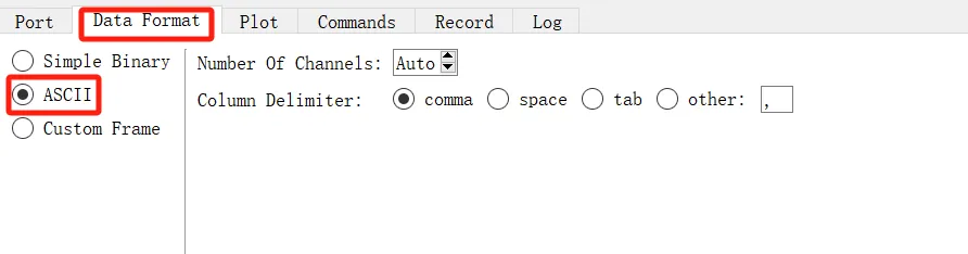
Select the data format ASCII for encoding, and leave other configurations as default:
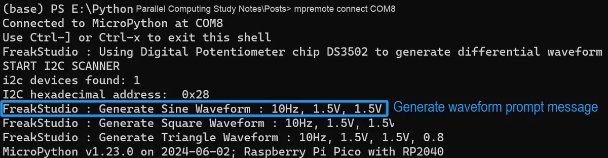
Burn the code, open a terminal, and use the mpremote tool to connect to the main controller; the output is as follows:
Open SerialPlot software, and you can see that the frequency and amplitude of the displayed DAC output voltage are both normal:
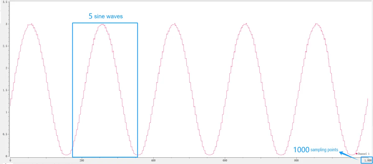
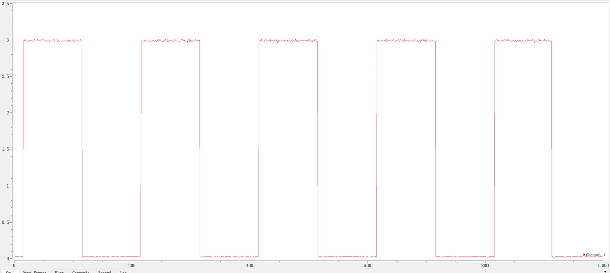
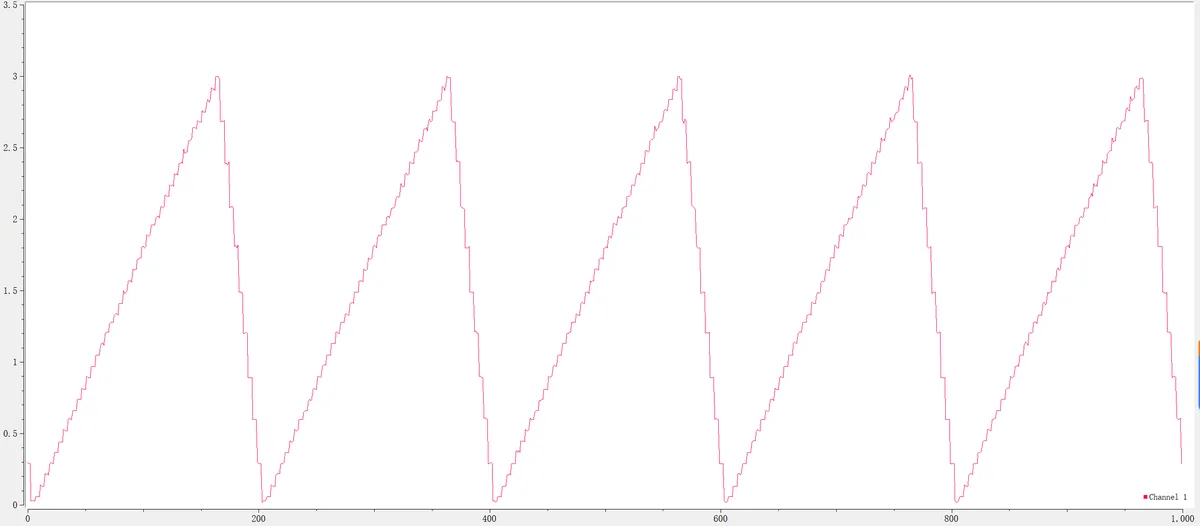
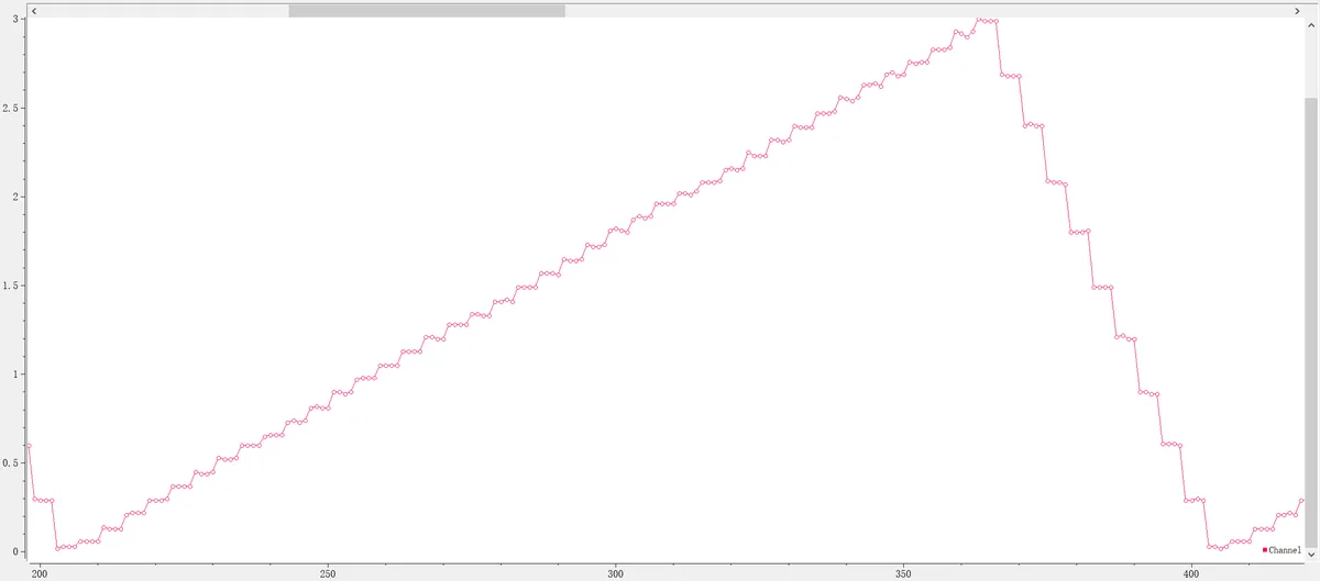
In the generated waveform, it can be seen that due to the low resolution (7-bit) of DS3502, the generated waveform has obvious steps, so it is not suitable for scenarios requiring high frequency or high precision.
IV. Drivers
ds3502_driver.zip 15 KB
5. BOM & Recommended Alternative Parts
None.
VI. Revision History
Document Version | Date of Revision | Modifier | Modified Content |
v1.0 | 2025-11-22 | Li Zisheng | Initialize the document The BOM sheet has not been finally checked, the driver has not been re-verified, and the 3.3 application experiment Not yet specified. |
v1.1 | 2025-12-29 | Li Zisheng | Added application experiments and production files |
v1.2 | 2025-12-31 | Xin Ruili | Create an open version of the document based on the internal document version v1.1. |
v1.3 | 2026-03-29 | Xin Ruili | Modified the application experiment section |
VII. Relevant Materials
7.1 Chip Datasheet
DS3502 Digital Potentiometer Datasheet.pdf 157 KB
7.2 Unique Icons for PCB Silkscreen