Contents
- I. Module Introduction
- II. Introduction to Major Chips
- 2.1 Chip Overview
- 2.2 Pin Definition
- 2.3 Functional Block Diagram
- 2.4 Performance Parameters
- 2.5 Reference Circuit
- 2.6 Chip Configuration
- 2.7 Communication Interfaces and Related Protocols
- 2.8 PCB Routing Precautions
- III. Circuit Engineering
- 3.1 Circuit Source Engineering
- 3.2 Module Usage Instructions
- 3.3 Application Experiment
- IV. Drivers
- 5. BOM & Recommended Alternative Parts
- VI. Revision History
- VII. Relevant Materials
- 7.1 Chip Datasheet
- 7.2 Unique Icons for PCB Silkscreen
I. Module Introduction
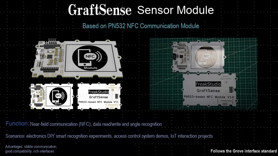
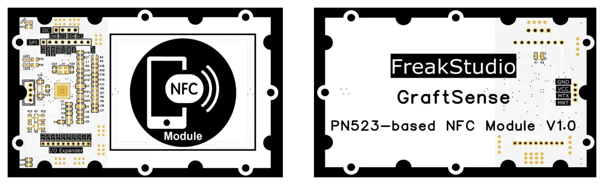
The PN532-based NFC communication module uses the PN5321A3HN/C106,55 as its main control chip, supports multiple communication modes including I2C, HUS, and SPI (switchable via pin configuration of SEL0 and SEL1), and is equipped with expansion interfaces, I2C interface, SPI interface, UART wiring terminals, etc. It also integrates a filter circuit, a crystal oscillator circuit, an antenna circuit, and a 5V-to-3.3V level conversion circuit.This module is an RFID reader that supports reading and writing Mi, UID, CUID, FUID, as well as bracelets and mobile phones with NFC function. It is compatible with 3.3V communication level, with the main communication mode being HSU (UART) at a baud rate of 115200. It is suitable for scenarios such as NFC tag reading and writing, access control identification, and mobile payment, providing a flexible and reliable hardware solution for near-field wireless communication applications.
II. Introduction to Major Chips
PN5321A3HN/C106,55 is a high-performance NFC controller chip from NXP, which supports the 13.56MHz frequency band, is compatible with multiple contactless protocols, and can implement modes such as card reader and card emulation. It is equipped with SPI, I2C, and UART interfaces, featuring high integration and low power consumption, and is suitable for near-field communication scenarios such as payment terminals and access control systems.
2.1 Chip Overview
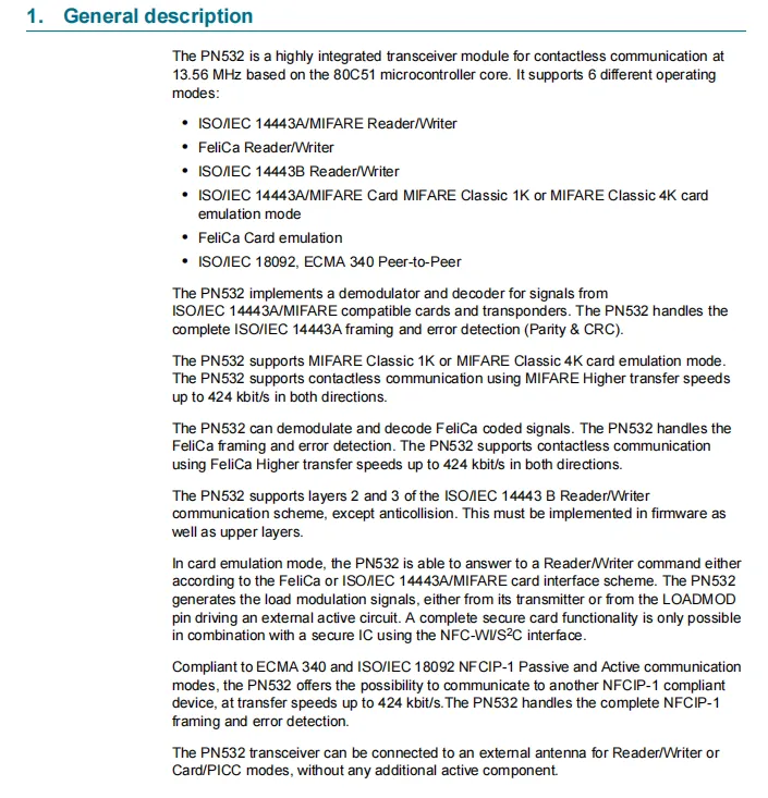
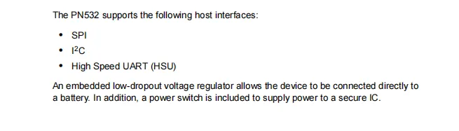
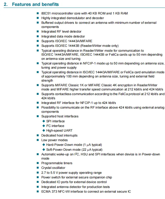
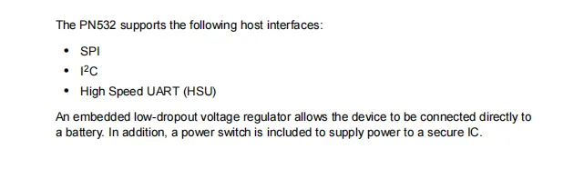

PN532 is a 13.56MHz contactless communication transceiver module based on the 80C51 microcontroller core. It supports 6 operating modes including card reader/writer, card emulation, and peer-to-peer communication, and is compatible with protocols such as ISO / IEC 14443A / MIFARE and Felica. It integrates functions such as demodulation/decoding and RF level detection, with a maximum communication rate of up to 424kbit/s;It supports SPI, I²C, and high-speed UART as three host interfaces, featuring a low-power mode, a wide 2.7-5.5V power supply range and other characteristics; it can also be externally connected to a security IC, making it suitable for scenarios such as mobile portable devices and consumer applications.
2.2 Pin Definition
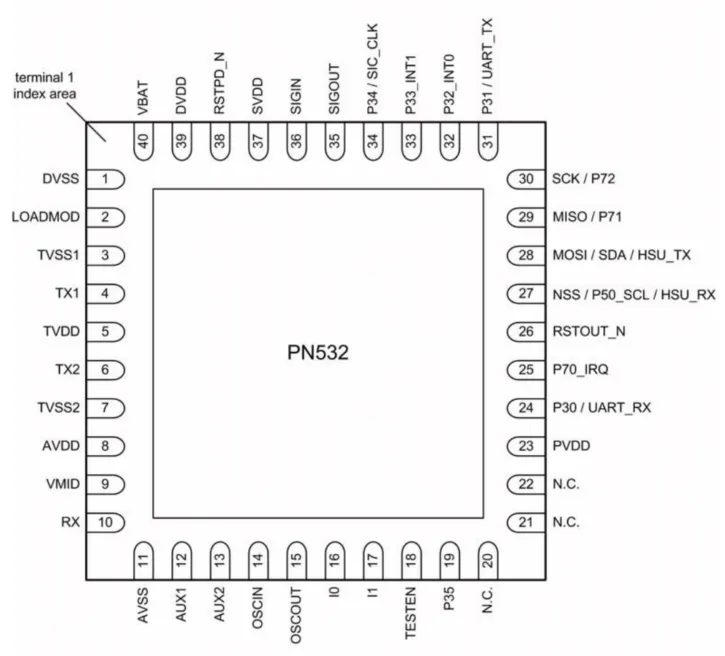
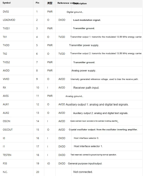
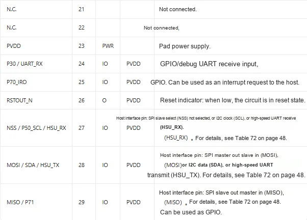
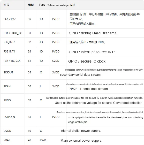
2.3 Functional Block Diagram
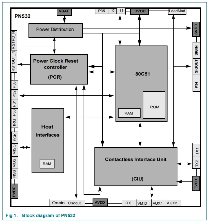
- Power Distribution Module (
Power Distribution): responsible for power distribution and management of all internal modules of the chip, ensuring reasonable power supply, such asVBAT,DVDD, etc. - Power Supply Clock Reset Controller (
Power Clock Reset controller,PCR): It manages the power supply, clock and reset logic of the chip, and coordinates clock synchronization and reset operations of each module. 80C51processor module: built-in withROMandRAM, it serves as the core arithmetic unit of the chip, responsible for executing instructions, processing data, and realizing the control and logical operation of the entire chip.- Host Interface Module (
Host Interfaces): Equipped withRAM, it provides communication interfaces with external hosts (such asSPI, etc.) to realize data interaction and instruction transmission between the chip and the external main controller. - Contactless Interface Unit (CIU): responsible for the contactless communication function, and transmits, receives and interacts with external contactless devices (such as NFC tags, etc.) through pins including
TX1,TX2andRX. - Clock and Analog Power Module:
Oscin,Oscoutprovide clock signals, andAVDDsupplies power to the analog circuit, ensuring the normal operation of the clock and analog parts of the chip.
Typical Scenarios (Taking NFC Communication as an Example):
- Communication initiation: The external host sends commands via the host interface →
80C51processor processes the command → controls theCIUunit to initiate contactless communication. - Data Interaction:
CIUtransmits signals viaTX1,TX2, and receives theRXsignal from an external NFC device → after being processed by80C51, the data is posted back to the external host through the host interface.
2.4 Performance Parameters
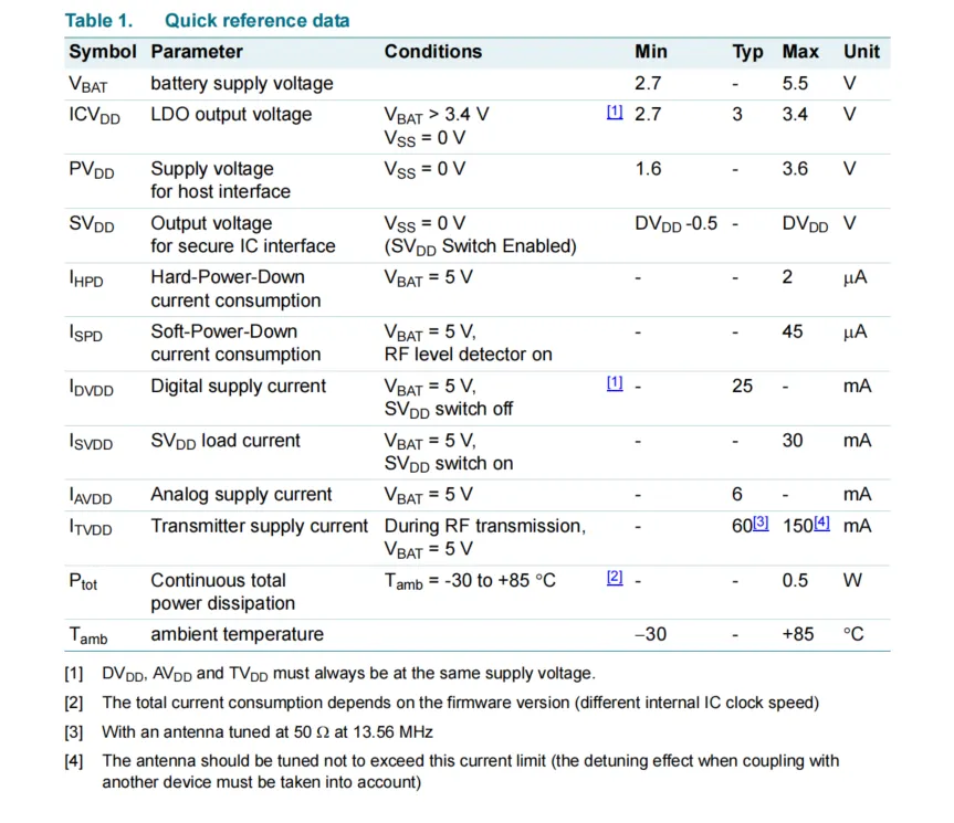
The key points in the table are as follows:
- Battery supply voltage (
V_BAT): 2.7~5.5V. LDOOutput Voltage (I_CVDD):V_BAT> 3.4V,V_SS= 0V: 2.7~3.4V.- Host interface supply voltage (
P_VDD):V_SS= 0V, 1.6~3.6V. - Safety
ICinterface output voltage (S_VDD):V_SS= 0V, when the switch is enabled, it ranges fromDVDD-0.5toDVDDV. - Power Consumption Current: Hard Power-Down Current (
I_HPD) max. 2μA; Soft Power-Down Current (I_SPD) max. 45μA; Digital Supply Current (I_DVDD) typ. 25mA;S_VDDLoad Current (I_SVDD) max. 30mA; Analog Supply Current (I_AVDD) typ. 6mA; Transmitter Supply Current (I_TVDD) typ. 60mA, max. 150mA. - Continuous total power consumption (
P_tot): Max. 0.5 W. - Ambient temperature (
T_amb): -30 to + 85°C.
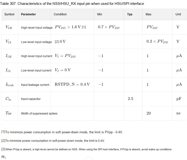
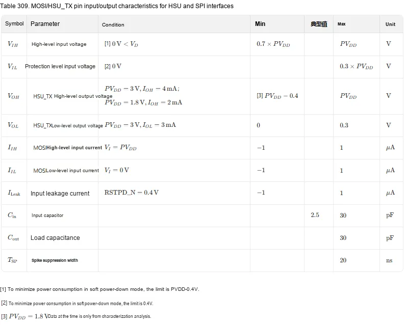
2.5 Reference Circuit
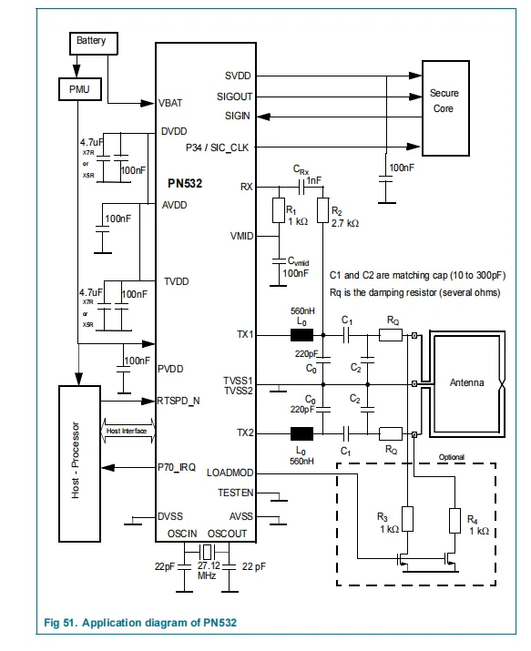
This is PN5321A3HN/C106,55 the application circuit of the chip, and the functions of each part are as follows:
- Power Supply and Filtering Section:
- The battery supplies
PMU(Power Management Unit) to provideVBATpower for the PN532. The peripheral 4.7μF and 100nF capacitors are used for power filtering, voltage stabilization and ripple interference reduction. DVDD,AVDD,TVDDand others supply power to different functional modules (digital, analog, transmitter) inside the chip respectively, ensuring the stable operation of each module.
- The battery supplies
- Clock Section:
- An external clock circuit is formed by connecting a 27.12MHz crystal oscillator and 22pF capacitors to
OSCINandOSCOUT, which provides the operating clock signal for the chip to ensure normal timing operation of the chip.
- An external clock circuit is formed by connecting a 27.12MHz crystal oscillator and 22pF capacitors to
- Host Interface Section:
- The PN532 communicates via pins including
PVD,RTS_PD_N, andP70_IRQto connect to an externalHost - Processor, enabling command interaction and data transmission between the chip and the host, so that the host can control the operating mode of the PN532.
- The PN532 communicates via pins including
- Non-contact communication interface section:
- Receive (RX): A receive matching circuit is formed by external components such as
Cpx,R₁,R₂, andCvmid, which processes the radio frequency signal received from the antenna and feeds it into the contactless interface unit inside the chip. - Transmission (TX1, TX2): An external transmission matching circuit is composed of
inductor L₀, capacitorC₁,C₂, damping resistorRQ, etc. The radio frequency signal generated inside the chip is amplified and matched, then transmitted through the antenna to realize communication with external contactless devices (such as NFC tags).
- Receive (RX): A receive matching circuit is formed by external components such as
- Security Core Interface Component:
SVDD,SIGOUT,SIGNpins are connected to theSecure Coreto implement security-related communication and data exchange, ensuring the security of contactless communication.
- Optional circuit section:
- The components within the dashed box, including
R₃,R₄and others, form an optional circuit that can be configured according to actual application scenarios (such as antenna tuning and damping control) to optimize communication performance.
- The components within the dashed box, including
2.6 Chip Configuration
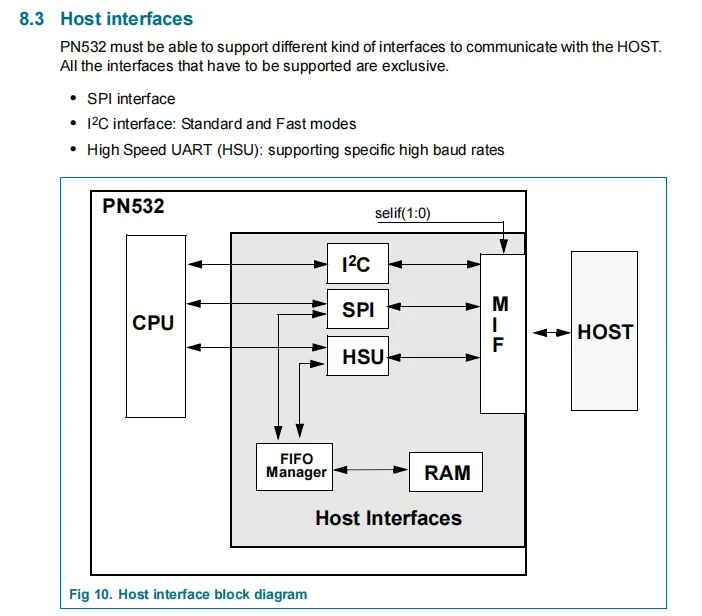
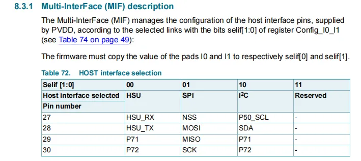
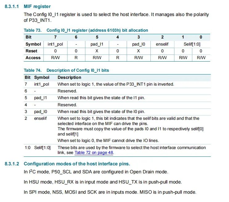
PN532 supports switching among three host interfaces: HSU, SPI, and I²C, which is implemented through the coordination of the pin levels of I0 / I1 and the Config I0_I1 register: first, the Config I0_I1 register reads the actual levels of the pad_I0 and pad_I1 bits corresponding to the I0 and I1 pins, then copies them to the selif[1:0] bits.Select the interface according to the combination of selif[1:0](00 corresponds to HSU, 01 corresponds to SPI, 10 corresponds to I2C). Meanwhile, set the enselif bit of the register to 1 to enable the MIF module to drive the corresponding pins; finally, the pins of different interfaces will automatically switch to the corresponding working modes (e. g. I²C is in open-drain mode, SPI is in input/push-pull mode), so as to complete the switching of the three Communication Protocols.
2.7 Communication Interfaces and Related Protocols
This paper mainly introduces the High-Speed Universal Asynchronous Receiver/Transmitter (HSU); as for IIC and SPI, only partial contents are presented herein. For relevant materials, please refer to the datasheet in the attachment.
2.7.1 High Speed Universal Asynchronous Receiver/Transmitter (HSU)
High-speed Universal Asynchronous Receiver/Transmitter (HSU) provides a high-speed link to the host (up to 1.288 Mbit/s).
HSU is a full-duplex serial port. Equipped with a receive buffer, this serial port, in combination with the FIFO manager, can receive multiple bytes without being restricted by the CPU real-time constraints. However, if the receive FIFO remains unread by the CPU and the number of received bytes exceeds the capacity of the receive FIFO, the newly incoming bytes will be lost.
Both the receive and transmit data registers of the HSU are accessed by firmware via the FDATA register of the FIFO manager. Writing data to FDATA loads the transmit register, while reading data from FDATA accesses the separate receive register.
This Universal Asynchronous Receiver/Transmitter (UART) features the following characteristics:
- Full-duplex serial port
- receive buffer that can receive new bytes while the previous bytes are being stored in the FIFO manager
- 8-bit data transmission
- Programmable baud rate generator with prescaler for transmission and reception
- Based on a 27.12 MHz clock
- Specialized Preamble Filter for Protocols
- Wake-up Generator
2.7.1.1 Operation Mode
HSU only supports one operating mode, which has the following characteristics:
- Start bit: A start bit is detected when a logic 0 appears on the HSU_RX line.
- 8 data bits:
- Data bits are transmitted or received in a least significant bit (LSB) first manner.
- Stop bit:
- During reception, a stop bit is detected when all data bits have been received and the stop bit is sampled as logic 1. The number of stop bits is programmable and can be either 1 or 2.
- During transmission, after the transmission of the complete data bits, a variable number of stop bits will be transmitted, and this number can be programmed to be between 1 and 4.
2.7.1.2 HSU Baud Rate Generator
To achieve high-speed transmission rates, the HSU has its own baud rate generator, which consists of a prescaler and a counter. The prescaler is located before the counter, and its function is to frequency-divide the count signal to expand the range of the counter (at the cost of reducing resolution). The division coefficient of the prescaler is equal to 2 to the power of HSU_PRE [8:0](see Table 113 on page 77), so the division coefficient ranges from 1 (2^0) to 256 (2^8). The combination of these two modules defines the bit duration and bit sampling.
2.7.1.3 HSU Preamble Filter
After three consecutive characters (00,00, FF) are received, the received characters will be sent to the FIFO manager. When a frame ends and before a new frame arrives, the firmware shall write a logic 1 to the frame start bit of the HSU_CTR register to reactivate the preamble filter. If the firmware does not write a logic 1, all characters of the frame, including the preamble, will be sent to the FIFO manager.
2.7.1.4 HSU Wakeup Generator
The HSU wake-up generator is a 3-bit counter that increments on each rising edge of the HSU_RX pin. When the counter reaches 5, the hsu_on signal is set to logic 1 to wake up the PN532. This module is extremely useful in soft power-down mode. Firmware should reset this counter by writing a logic 1 to the res_wu bit of the HSU_CTR register before entering soft power-down mode.
2.7.1.5 HSU_STA Register
The special function register (SFR) HSU_STA is the status register of the HSU.
HSU_STA Register (SFR: Address ABh) Bit Allocation
| Bit | 7 | 6 | 5 | 4 | 3 | 2 | 1 | 0 |
| Symbol | set_bit | - | - | disable_preamb | irq_rx_over_en | irq_rx_fer_en | irq_rx_over | irq_rx_fer |
| Reset | 0 | 0 | 0 | 0 | 0 | 0 | 0 | 0 |
| Access | RW | R | R | RW | RW | RW | RW | RW |
HSU_STA bit description
| Bit | Symbol | Description |
| 7 | set_bit | During a write operation, if set to logic 0, bits set to logic 1 in the write command are written as logic 0 to the register; if set to logic 1, bits set to logic 1 in the write command are written as logic 1 to the register. |
| 6 to 5 | - | Reserved |
| 4 | disable_preamb | Preamble filter disable. When set to logic 1, this bit disables preamble filtering, i.e. any byte received on the HSU_RX line is transferred to the FIFO manager. |
| 3 | irq_rx_over_en | FIFO overflow interrupt enable. When set to logic 1, this bit enables interrupt generation when irq_rx_over is set to logic 1. Bit IE1_5 of register IE1 must also be set to logic 1 to enable the corresponding CPU interrupt. |
| 2 | irq_rx_fer_en | Framing error interrupt enable. When set to logic 1, this bit enables interrupt generation when irq_rx_fer is set to logic 1. Bit IE1_5 of register IE1 must also be set to logic 1 to enable the corresponding CPU interrupt. |
| 1 | irq_rx_over | Receive FIFO overflow interrupt. Set to logic 1 when the FIFO manager is full (rcv_jack set to logic 0) and the HSU shift register is ready to send another byte to the FIFO manager. |
| 0 | irq_rx_fer | Framing error interrupt. Set to logic 1 when a framing error is detected. Framing error detection is based on stop bit sampling. This bit is set to logic 1 when the stop bit is expected to be logic 1 but is sampled as logic 0. |
2.7.1.6 HSU_CTR Register
This register controls the configuration of the HSU.
Bit allocation of HSU_CTR register (SFR: address ACh)
| Bit | 7 | 6 | 5:04 | 3 | 2 | 1 | 0 |
| Symbol | hsu_wu_en | start_frame | tx_stopbit[1:0] | rx_stopbit | tx_en | rx_en | soft_reset_n |
| Reset | 0 | 0 | 0 | 0 | 0 | 0 | 1 |
| Access | RW | RW | RW | RW | RW | RW | RW |
HSU_CTR bit description
| Bit | Symbol | Description |
| 7 | hsu_wu_en | HSU wake-up enable. When set to logic 1, this bit re-activates the NSS/SCL/HSU_RX rising edge counter. When the counter reaches 5, the hsu_on signal is activated. This signal is one of the possible wake-up event signals in the PCR module. Firmware should set this bit in the PCR register to logic 1 before requesting soft power-down mode. In soft power-down mode, bit HSU_on_en of the PCR wake-up register (see Table 144 on page 97) must also be set to logic 1 to enable the corresponding PN532 wake-up. |
| 6 | start_frame | Enable the preamble filter for the current frame. When set to logic 1, this bit indicates that a new frame is about to arrive. This re-activates the preamble filter (if enabled), meaning the first three "00 00 FF" characters are not sent to the FIFO manager. |
| 5:04 | tx_stopbit[1:0] | Defines the number of stop bits during transmission. These two bits define the number of stop bits inserted at the end of a transmitted frame. The number of stop bits transmitted equals tx_stopbit + 1. |
| 3 | rx_stopbit | Defines the number of stop bits during reception. This bit defines the number of stop bits expected at the end of a received frame. The number of stop bits expected during reception equals rx_stopbit + 1. |
| 2 | tx_en | Enable HSU transmission. When set to logic 1, this bit enables character transmission. When set to logic 0, transmission is disabled only after the current transfer completes. |
| 1 | rx_en | Enable HSU reception. When set to logic 1, this bit enables character reception. When set to logic 0, reception is disabled only after the current reception completes. |
| 0 | soft_reset_n | HSU reset. When set to logic 0, this bit disables the clocks of the HSU_RX control, HSU_TX control and baud rate generator modules. |
2.7.1.7 HSU_PRE Register
This register is used to configure the prescaler of the baud rate generator. The prescaler can expand the range of the counter at the cost of reducing resolution. The division coefficient of the prescaler ranges from 1 (2^0) to 256 (2^8).
Table 115. Bit Allocation of HSU_PRE Register (SFR: Address A4h)
| Bit | 7 | 6 | 5 | 4 | 3 | 2 | 1 | 0 |
| Symbol | 0 | 0 | 0 | hsu_prescaler[7:0] | 0 | 0 | 0 | 0 |
| Reset | 0 | 0 | 0 | 1 | 0 | 0 | 0 | 0 |
| Access | RW | RW | RW | RW | RW | RW | RW | RW |
HSU_PRE bit description
| Bit | Symbol | Description |
| 7 to 0 | hsu_prescaler[7:0] | Combined with HSU_CNT, defines the HSU baud rate. Baud rate = fclk / ((hsu_prescaler + 1) * hsu_counter) |
2.7.1.8 HSU_CNT Register
This register is used to configure the counter of the baud rate generator.
Bit allocation of HSU_CNT register (SFR: address A5h)
| Bit | 7 | 6 | 5 | 4 | 3 | 2 | 1 | 0 |
| Symbol | 0 | 0 | 0 | hsu_counter[7:0] | 0 | 0 | 0 | |
| Reset | 0 | 0 | 0 | 1 | 0 | 0 | 0 | 0 |
| Access | RW | RW | RW | RW | RW | RW | RW | RW |
Table 118. Bit Description of HSU_CNT
| Bit | Symbol | Description |
| 7 to 0 | hsu_counter[7:0] | Combined with HSU_PRE, defines the HSU baud rate. Baud rate = fclk / ((hsu_prescaler + 1) * hsu_counter) |
The following is the recommended table for HSU data rates:
Table 119. Recommended HSU Data Rate Table
| Target data rate | HSU_CNT value | HSU_PRE value | Actual HSU data rate | Minimum recommended host HSU frequency | Maximum recommended host HSU frequency |
| 9600 | 0x71 | 0x18 | 9516 | 9326 | 9706 |
| 19200 | 0x9D | 0x0B | 19189 | 18592 | 19726 |
| 38400 | 0x65 | 0x06 | 38363 | 37610 | 39126 |
| 57600 | 0x9D | 0x02 | 57579 | 56428 | 58730 |
| 115200 | 0xEB | 0x00 | 115404 | 113096 | 117712 |
| 230400 | 0x76 | 0x00 | 229831 | 225234 | 234427 |
| 460800 | 0x3B | 0x00 | 459661 | 450467 | 468854 |
| 921600 | 0x1D | 0x00 | 959172 | 916468 | 963875 |
| 1288000 | 0x15 | 0x00 | 1291429 | 1265600 | 1317257 |
2.7.2 IIC Communication
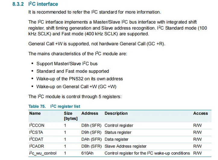
This section describes the PN532 I2C interface: it is a master/slave mode I2C bus interface (with built-in shift register, timing generation, and slave address recognition functions), supporting the 100kHz I2C standard mode and 400kHz fast mode; it supports wake-up via the " General Call + W " command, but does not support the hardware version of General Call (GC+ R).
Its I2C interface has the following key features: it supports master/slave I2C bus, is compatible with standard/fast modes, can wake up the PN532 via its own address, and can wake up the device with the " General Call + W " command.
In addition, this I2C module is controlled by 5 readable and writable registers, including the control register (I2CCON), the status register (I2CSTA), the data register (I2CDAT), the slave address register (I2CADR), and the I2C wake-up condition control register (I2C_wu_control).
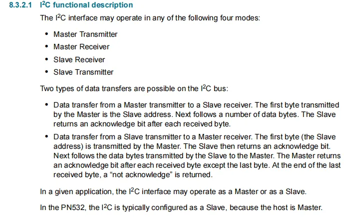
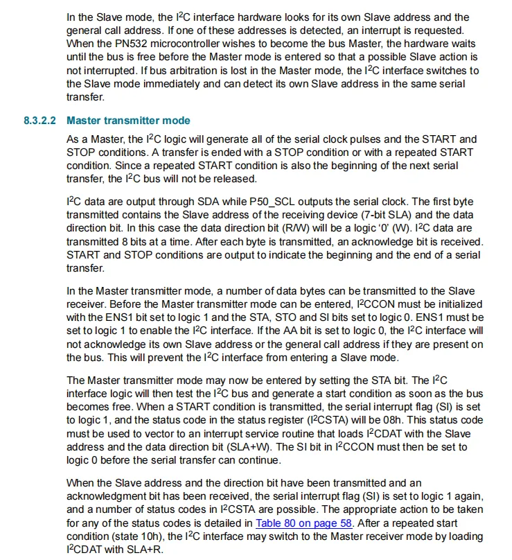
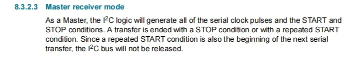
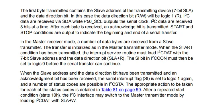
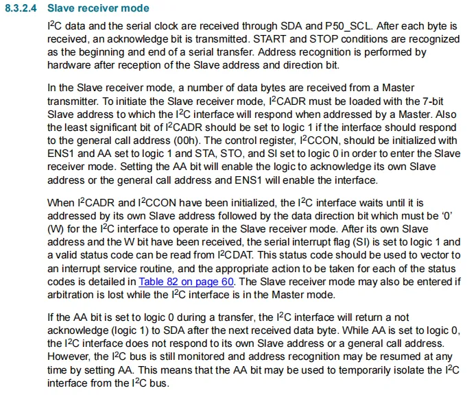
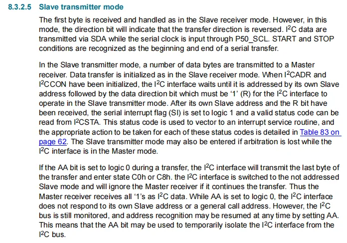
PN532 I2C supports four modes: master transmit, master receive, slave receive, and slave transmit, and features two transmission modes: "master sends data to slave (the master sends the slave address first, and the slave acknowledges byte by byte)" and "slave sends data to master (the master sends the slave address first, the slave sends data after acknowledging, and the master acknowledges byte by byte except for the last byte)"; in practical applications, the PN532 I2C is usually configured as a slave. In slave mode, it monitors its own address and the general call address to trigger an interrupt, and can also switch to master mode when the bus is idle; if arbitration is lost in master mode, it will switch back to slave mode.In the master transmission mode, PN532 generates clocks and start/stop signals. It is required to initialize the registers before entering this mode, first transmit the "slave address + write bit", and receive an acknowledgment after each byte transmitted; the entire process is handled via interrupts and status codes.
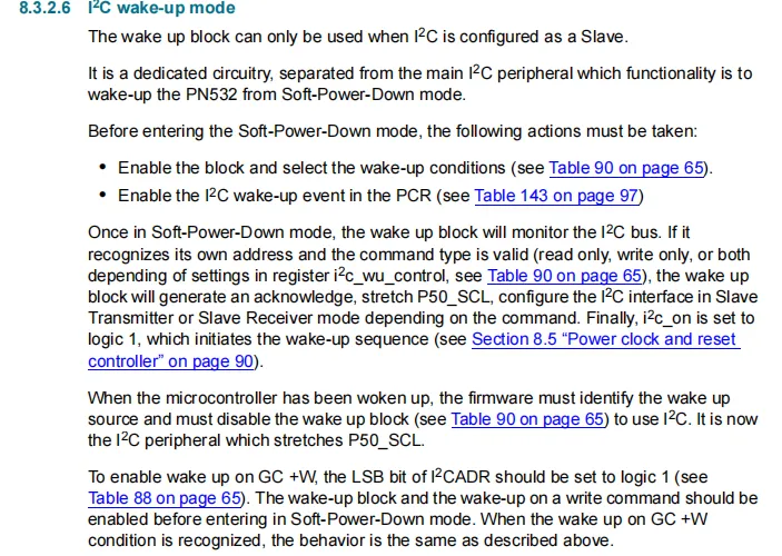
PN532 's I2C wake-up mode is only available when its I2C is configured as a slave, and it is a dedicated circuit designed to wake the device from soft power-down mode; before entering soft power-down, this wake-up module must be enabled, the wake-up condition selected, and the PCR has the I2C wake-up event enabled; during soft power-down, this module monitors the I2C bus, and after recognizing its own address and a valid command, it generates an acknowledge, pulls low SCL, configures I2C as slave transmit/slave receive mode and triggers wake-up; after wake-up, the firmware must identify the wake-up source and disable this module before the normal I2C can be used;To enable GC+ W wake-up, you need to set the I2CADR LSB to 1, and enable the write command wake-up function before entering soft power-down mode.
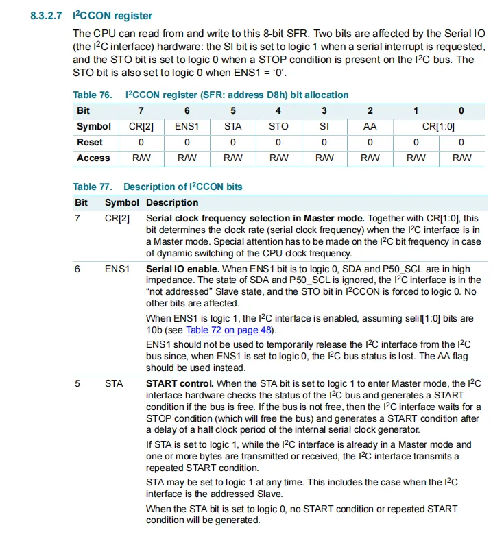
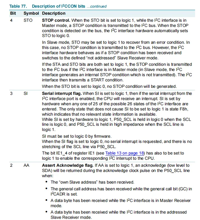
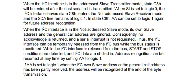
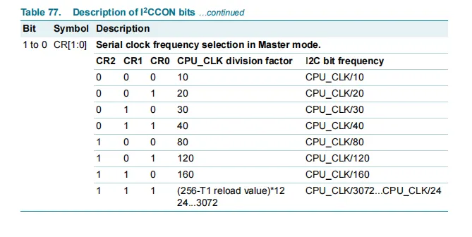
I2CCON is an PN532 8-bit read-write register used to control the core logic of the I2C interface: among them, CR[2] and CR1[1:0] jointly determine the clock frequency in master mode;ENS1 controls the enable of the I2C interface (set to 0 to disable the interface and put it in high-impedance state, set to 1 to enable it);STA controls the start condition (setting it to 1 in master mode will detect bus idle and generate a start signal);STO controls the stop condition (setting it to 1 in master mode sends a stop signal, which can be used for error recovery in slave mode);SI is the serial interrupt flag (hardware sets it to 1 to trigger an interrupt, which requires firmware to set it back to 0);AA is the acknowledge flag (when set to 1, it will return an acknowledge in scenarios such as receiving its own address and general call address), and these bits collectively implement the enable, clock, start/stop control, interrupt and acknowledge management of I2C.
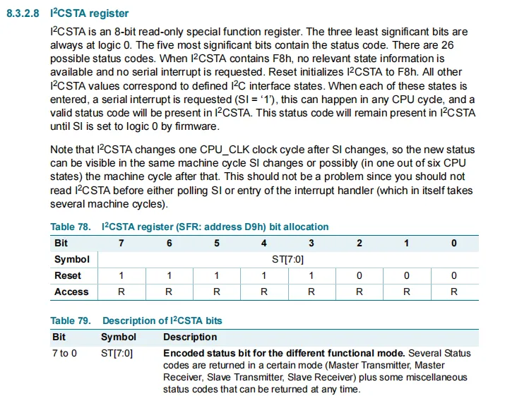
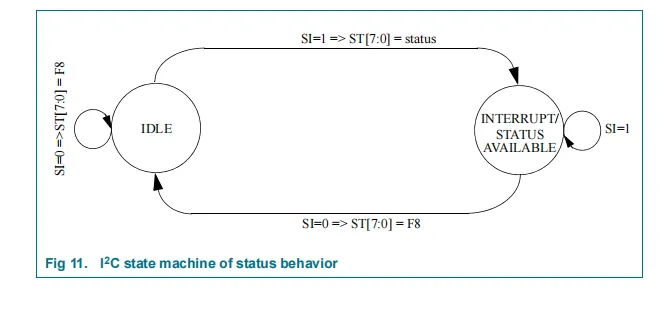
I2CSTA is an PN532 8-bit read-only register: its lower 3 bits are fixed to 0, and the upper 5 bits store the status codes of the I2C interface (there are 26 types in total, and the value after reset is F8h, indicating no valid status); when I2C enters the corresponding status, hardware will set the SI interrupt flag to 1. At this point, I2CSTA presents a valid status code and triggers an interrupt, and this status code will remain until the firmware clears SI to 0. Its status change lags behind that of SI by one CPU cycle.
The corresponding finite-state machine logic is: in idle state, SI = 0, and I2CSTA is F8h; when SI = 1, it enters the "interrupt / status available" state, and I2CSTA loads the corresponding status code; after firmware processing, SI is set to 0, and the system returns to the idle state.
2.7.3 SPI Communication
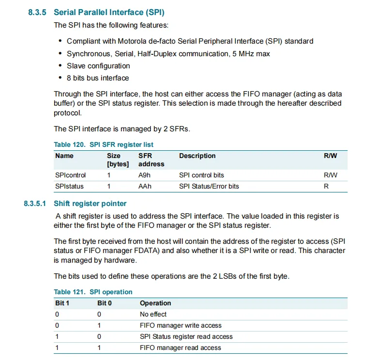
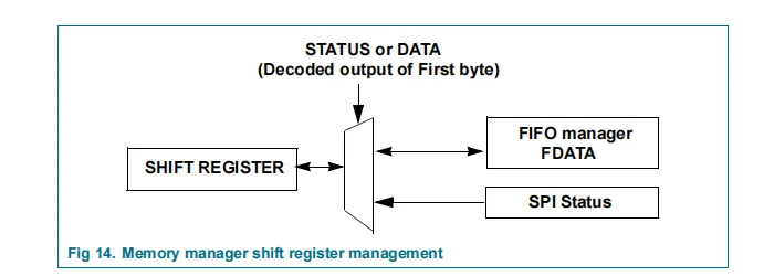
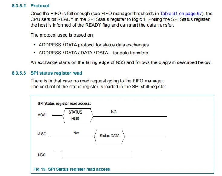
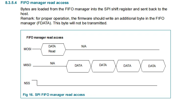
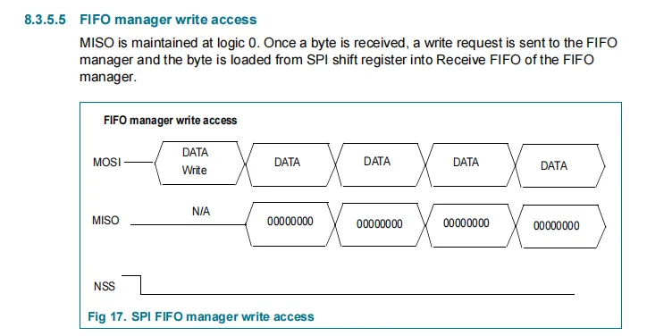
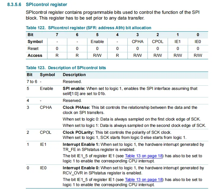
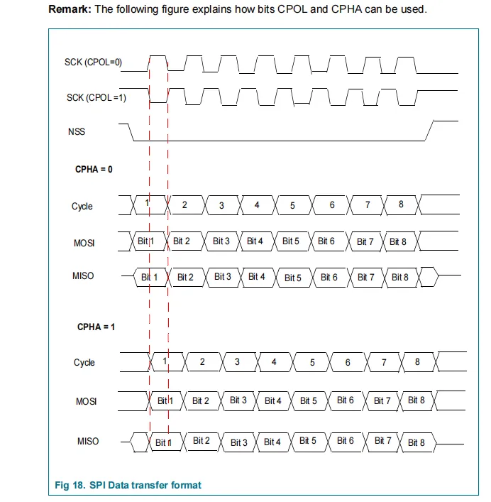
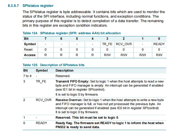
PN532 SPI Communication: It operates in slave mode, complies with Motorola SPI standard, and supports synchronous half-duplex 8-bit bus communication (max. 5MHz), which is managed by two registers: SPIControl (for control enable, clock phase/polarity, and interrupt) and SPIstatus (for monitoring the FIFO empty, overflow, and ready status).
Communication selects operations (write FIFO, read status, read FIFO, etc.) via the lower 2 bits of the first byte, and is initiated by the falling edge of NSS; when reading the status, the status is loaded into the shift register and returned, reading FIFO means fetching data from the FIFO and sending it to the host, writing FIFO means the host sends data to be stored in the receive FIFO (with MISO held at 0);SPIstatus the "ready" flag is set to 1 by the firmware to prompt the host that data transmission is available.
2.8 PCB Routing Precautions
None.
III. Circuit Engineering
3.1 Circuit Source Engineering
To obtain the source project of the circuit, please follow the official account [Freak Embedded]
3.2 Module Usage Instructions
SCH_Schematic1_BeiDou Navigation Module Based on Air530Z-V1.0.0_2025-11-10.pdf 2.2 MB
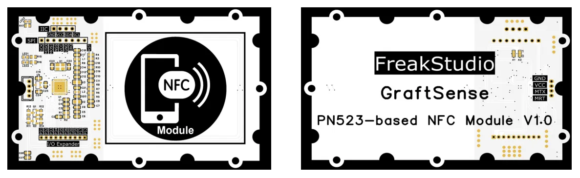
In this module, MRX (corresponding to the UART RXD pin of the MCU) is physically connected to the PN5321A3HN/C106,55 TXD pin, and MTX (corresponding to the UART TXD pin of the MCU) is physically connected to the PN5321A3HN/C106,55 RXD pin;This is because UART serial communication follows the "cross-transmit-receive" rule — the transmit end (TX) of both communication parties needs to be connected to the receive end (RX) of the other party; this design ensures correct bidirectional transmission of UART serial data between the MCU and PN5321A3HN/C106,55.
It is particularly important to note that when using this module, MRX is directly connected to the UART RXD of the MCU, and MTX is directly connected to the UART TXD of the MCU. Do not cross-connect them under any circumstances.
NFC (Near Field Communication) is a short-range wireless technology operating at 13.56 MHz with a communication distance of no more than 4 centimeters, jointly developed by Philips (now NXP), Nokia and Sony. It is essentially an upgraded version of RFID (Radio Frequency Identification) technology, but integrates the three functions of reader, card and peer-to-peer communication onto a single chip.

NFC has three operating modes:
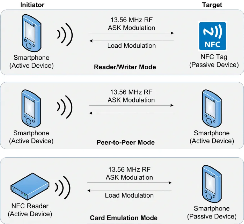
- Card mode: The device functions as an
ICcard. For example, you can still tap to pay for public transport or access controlled areas even when your phone is out of power (powered by the card reader); - Reader/writer mode: The device acts as a card reader to read
NFCcard information (PN532commonly uses this mode); - Peer-to-peer mode: two
NFCdevices transmit data directly (e. g., a phone transferring photos).
The main categories of NFC cards are as follows:
| Protocol type | Common name | Common card examples | Typical use |
| ISO/IEC 14443 Type A | Type A card | Mifare Classic (S50/S70), Mifare Ultralight | Access cards, campus cards, NFC stickers |
| ISO/IEC 14443 Type B | Type B card | ID cards, some bank IC cards | Government, finance |
| ISO/IEC 15693 | Long-range card | I-Code series | Product traceability, warehouse management |
| Felica | Sony card | Suica (Japanese transit card), Felica Lite | Japanese payment, transit |
To ensure compatibility across devices such as mobile phones, NFC Forum has defined Tag 1 to Tag 5 five types of tags, which are essentially "wrappers" for the aforementioned protocols:
| Tag type | Underlying protocol | Features | Common uses |
| Tag1 | Type A | Low cost, small capacity | Disposable tags |
| Tag2 | Type A | Rewritable, small capacity | NFC stickers (most common) |
| Tag3 | Felica | High security | Japanese devices |
| Tag4 | Type A/B | Large capacity, strong encryption | Financial IC cards, high-end access control |
| Tag5 | ISO15693 | Long-range identification | Product tags |
Classified by encryption capability (which determines whether read/write operations are supported), NFC cards can be categorized into the following types:
- Unencrypted / weakly encrypted cards: such as
Mifare Ultralight,Topaz, which have no hardware encryption and are suitable forNFCstickers; - Encrypted logic encrypted card: e. g.
Mifare Classic (S50/S70), which features simple password protection (default password:0xFFFFFFFFFFFF); - Smart
CPUcards: such asMifare DESFire, ID cards, with built-inCPUand operating system, featuring extremely high security.
PN532 is a multifunctional NFC chip from NXP, built on the 8051 microcontroller, supporting 6 operation modes and 3 host interfaces (SPI / I2C / USART), making it the top choice for DIY enthusiasts. PN532 supports almost all mainstream NFC cards, as it can emulate a wide range of card readers:
- Fully supports
ISO/IEC 14443 Type A(the most commonly used):Mifare ClassicSeries:S50(1K),S70(4K) — common cards used for residential access control and company employee badgesMifare Ultralightseries:UltraLight,UltraLight C——NFCstickers, disposable tickets;Topaz/Jewel:Tag1tag card.
- Supports
ISO/IEC 14443 Type B:- It can read ID cards and some bank
ICcards, but the corresponding key and parsing logic are required to obtain complete information.
- It can read ID cards and some bank
- Supports
ISO/IEC 15693:- Reads
I-Codeseries cards, suitable for warehouse inventory and commodity anti-counterfeiting.
- Reads
- Supports
Felica:- Capable of reading Japanese-standard
FeliCacards (such as Japanese transit cards), making it suitable for compatibility projects involving Japanese-brand devices.
- Capable of reading Japanese-standard
- Fully support
NFC Forum Tag 1 to Tag 5- It supports reading and writing to both low-cost
NFCstickers (Tag2) and high-end financialICcards (Tag4).
- It supports reading and writing to both low-cost
However, there are also some NFC cards that PN532 does not support:
- Low-frequency
RFIDcards: 125kHz/134.2kHz (e. g., old-style access control cards likeEM4100); - UHF
RFIDCard: 860~960MHz (for logistics); - Non-standard private protocol card: A niche card that does not conform to the four mainstream protocols listed above.
Simply put, PN532 only supports IC cards rather than ID cards:
| Comparison | IC card | ID card |
| Operating frequency | Mostly 13.56MHz (high frequency) | Mostly 125kHz (low frequency) |
| Read/write characteristics | Readable and writable, with built-in memory chip and encryption logic | Read-only, stores only a fixed unique card number, no storage / write capability |
| Security attributes | Supports encryption algorithms (e.g. MIFARE encryption logic), enables data exchange | No encryption, card number easily copied, identification only |
| Core function | Identification + data storage / transactions (e.g. access control + payment) | Basic identification only (e.g. plain access control, attendance) |
We can make a distinction through the following methods:
- Check the labels / instructions:
ICcards are usually marked withISO/IEC 14443,MIFARE,NFCand other words;IDcards are mostly marked withEM4100,125kHz,read-only IDand the like. - Read-write test: Use the corresponding card reader to try writing small amounts of data (such as access control permissions); those that support writing are
ICcards; those that can only read the card number but cannot write data areIDcards.
Also, when using PN532, the following points should be noted:
PN532can only read and writeNFCcards with known or default passwords, and cannot crack encrypted cards:The default password for Mifare Classiccards is0xFFFFFFFFFFFF(for all blocks except block 0);- If the card password is modified, the corresponding block cannot be accessed without the correct password;
- The stronger the encryption of the card (such as
CPUcards), the more complex the required keys and permissions will be.
PN532cannot duplicate all cards:- Cannot duplicate the encrypted card: unless all block ciphers remain unmodified (which is practically impossible);
- Non-duplicable
UIDunchangeable cards: Many access control systems verify the uniqueIDof the card; - Copying is only applicable to: default passwords, and simple access control/attendance cards without special encryption.
PN532can emulate a card, but there is a key limitation:- Simulated card
ID(4 bytes): the first byte is fixed at0x08; - This means the original card cannot be perfectly copied
ID, and many access control systems will reject such emulated cards.
- Simulated card
3.3 Application Experiment
Here, we use the GraftPort-RP2040 development board for testing, and the PN532-based NFC communication module uses the UART interface to communicate with the main controller.
Here, we first use the HY2.0-4P cable to connect the module to the GraftPort-RP2040 development board's UART0 interface:
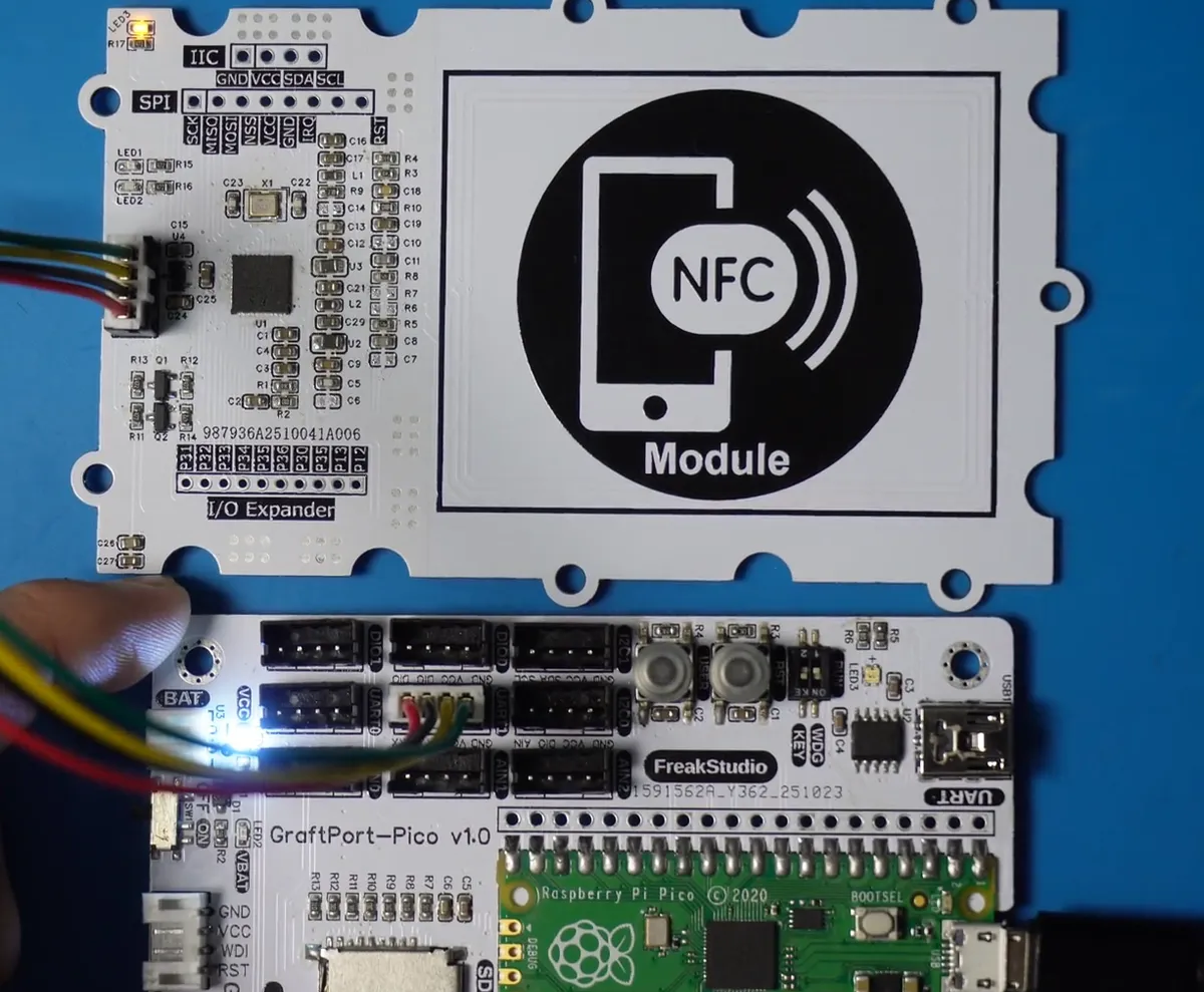
The module connections are shown in the following table:
Development Board Pins | Module Pins | Description |
Pin 8 |
|
|
Pin 9 |
|
|
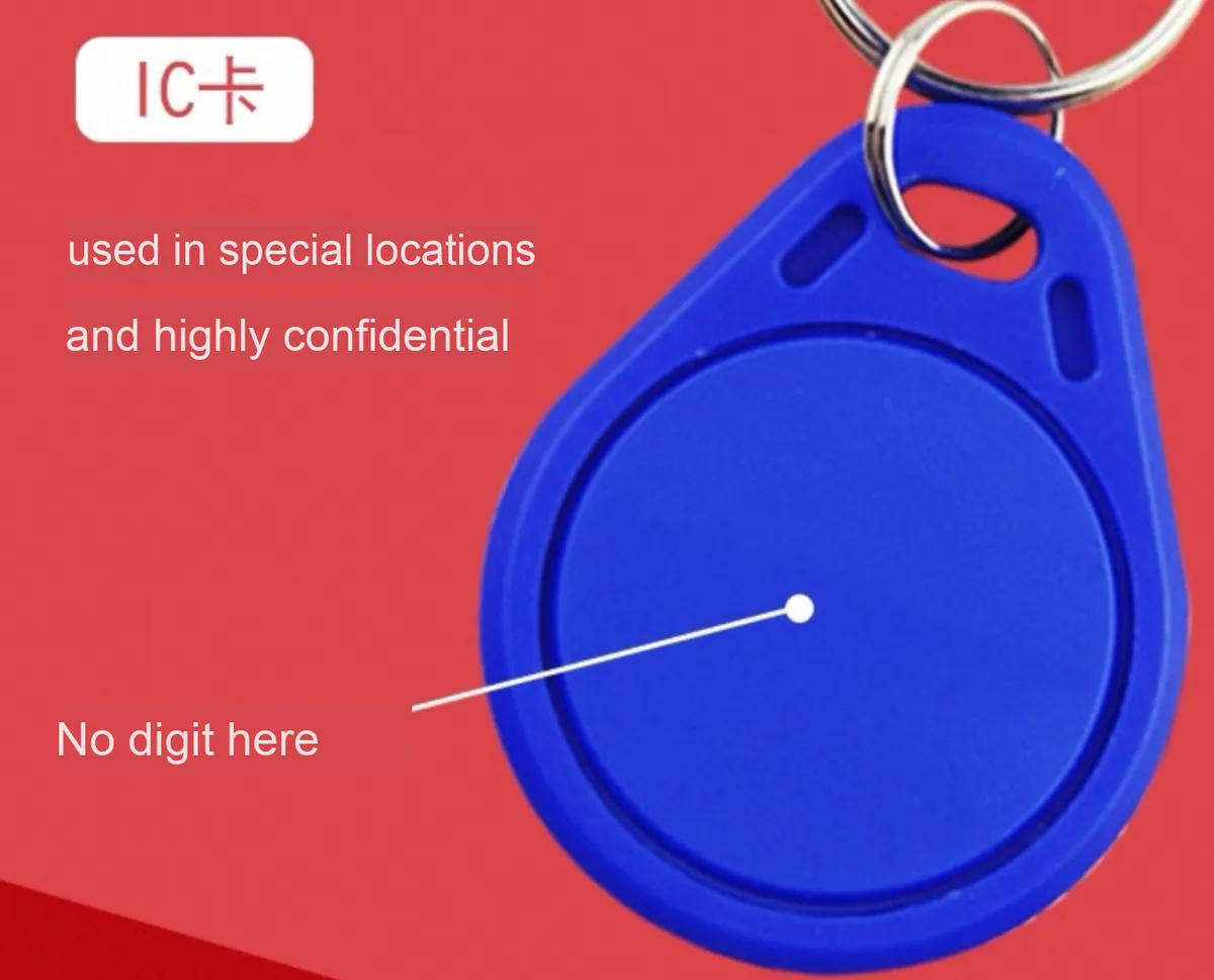
At the same time, we also need to purchase one in advance IC card for read-write verification test:
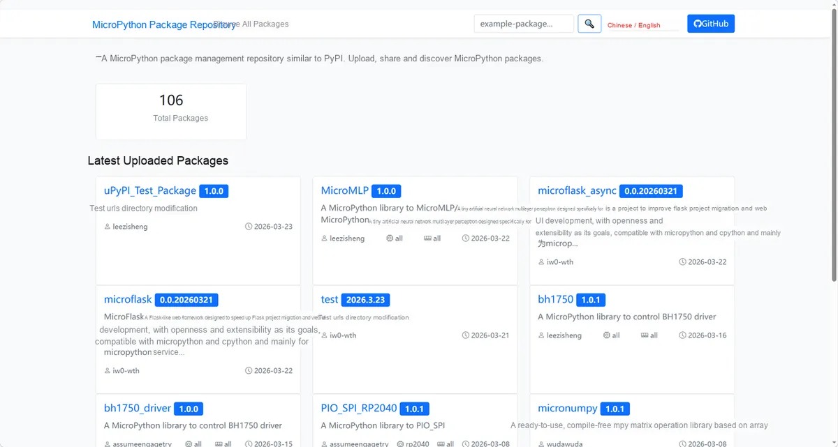
Here, we need to search for the relevant driver packages on uPyPI: https://upypi.net/zh/
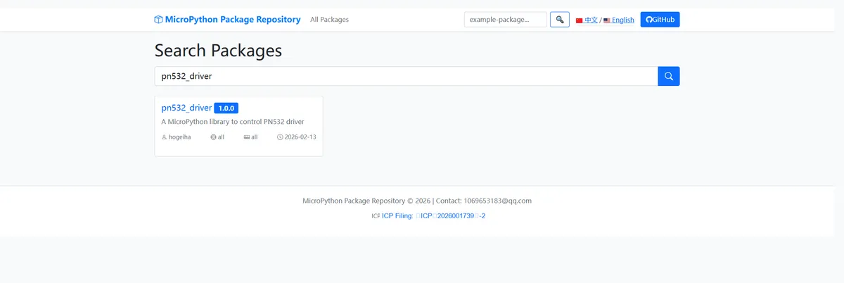
Enter pn532_driver to search, and the following will be displayed:
Click to copy the local installation command:
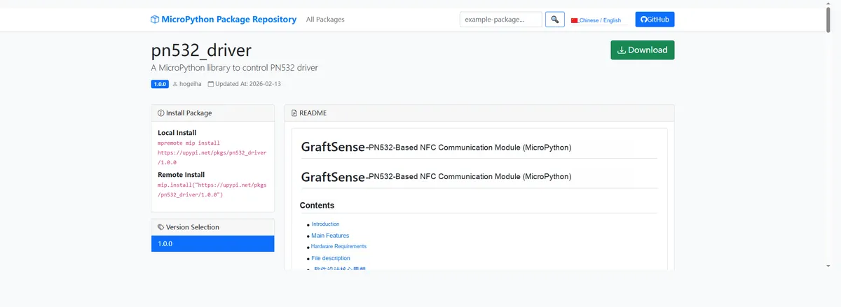
Import the module driver library code via the mip tool. Below are the usage commands for the mpremote tool:
mpremote mip install https://upypi.net/pkgs/pn532_driver/1.0.0Import the PN532 NFC module driver - MicroPython test code, then copy the following main.py code into our project:
# MicroPython v1.23.0
# -*- coding: utf-8 -*-
# @Time    : 2025/9/4 3:50 PM
# @Author  : 缪贵成
# @File    : main.py
# @Description : Driver test file for the PN532-based NFC module. Tests Mifare Classic cards (e.g., transit cards): ID reading, Block4 authentication, read/write

# ======================================== Import Modules =========================================

import time
from machine import UART, Pin
from uart import PN532_UART
from pn532 import MIFARE_CMD_AUTH_A

# ======================================== Global Variables ============================================

# ======================================== Functions ============================================

# ======================================== Custom Classes ============================================

# ======================================== Initialization configuration ===========================================

time.sleep(3)
print("FreakStudio: Test NFC module functionality")

# UART initialization (adjust to the actual hardware pins)
uart = UART(1, baudrate=115200, tx=Pin(8), rx=Pin(9))
# Optional: Reset pin
# reset_pin = Pin(15, Pin.OUT)

# Create a PN532 instance
nfc = PN532_UART(uart, reset=None, debug=True)

# Initialize the PN532
print("Initializing PN532...")
# nfc.reset()

# Get the firmware version
try:
    version = nfc.firmware_version
    print("PN532 firmware version:", version)
except RuntimeError as e:
    print("Failed to read firmware version:", e)
    time.sleep(3)

# Configure SAM (for card reading)
nfc.SAM_configuration()
print("PN532 SAM configured")
time.sleep(3)

# ======================================== Main Program =============================================

while True:
    try:
        print("---- Waiting for card (Mifare Classic) ----")
        uid = nfc.read_passive_target(timeout=1000)

        if uid is None:
            print("No card detected")
            time.sleep(2)
            continue

        print("Card detected UID:", [hex(i) for i in uid])
        time.sleep(2)

        # ==================== Mifare Classic Test ====================
        key_default = b"\xFF\xFF\xFF\xFF\xFF\xFF"
        block_num = 4

        if nfc.mifare_classic_authenticate_block(uid, block_num, MIFARE_CMD_AUTH_A, key_default):
            print(f"Block {block_num} authentication successful")
            time.sleep(1)

            data = nfc.mifare_classic_read_block(block_num)
            if data:
                print(f"Read block {block_num} data:", [hex(i) for i in data])
            time.sleep(1)

            test_data = bytes([0x01] * 16)
            if nfc.mifare_classic_write_block(block_num, test_data):
                print(f"Successfully wrote block {block_num}: {[hex(i) for i in test_data]}")
            time.sleep(1)
        else:
            print(f"Block {block_num} authentication failed")
            time.sleep(1)

        # ==================== Low Power Test ====================
        print("Entering low power mode...")
        if nfc.power_down():
            print("PN532 entered low power mode")
        time.sleep(2)

        print("Waking up...")
        nfc.reset()
        print("Wake up complete")
        time.sleep(2)

    except Exception as e:
        print("Error:", e)
        time.sleep(2)
In the code above, it is mainly used to verify the interaction capability of Mifare Classic type IC cards: the program first initializes the PN532 module, obtains its firmware version and configures the card reading mode, then waits for a card in a loop. After detecting a card, it reads the card's unique identifier UID, then authenticates the 4th Block Storage area of the card with the default key. After the authentication is completed, it reads the data of this area, writes test data, and finally tests the low-power mode switching of the module (waking it up after entering low-power mode).
To flash the code, open a terminal and use the mpremote tool to connect to the main controller; the output is as follows:
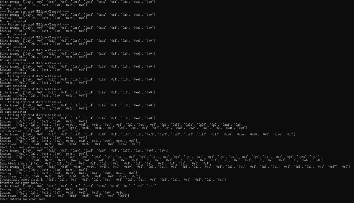
It can be seen that when our IC card is placed on top of the module, the Raspberry Pi Pico successfully reads the NFC and prints the result to the terminal:
As can be seen from the terminal output, the program repeatedly executes the "wait for card - detect card" loop, and no card is detected in some rounds (displayed as No card detected);When a Mifare Classic card is detected, the card's UID is successfully read, authentication of Block4 is completed using the default key, after reading the original data of this block, test data consisting entirely of 0x01 is written, then the PN532 is successfully made to enter low-power mode and wake up, which practically verifies the functional validity of the PN532 in terms of target IC card identification, storage area authentication, data read/write, and power consumption control.
IV. Drivers
pn532_driver.zip 19 KB
5. BOM & Recommended Alternative Parts
None.
VI. Revision History
Document Version | Date of Modification | Modifier | Modified Content |
v1.0 | 2025-11-11 | Ling Gaoxing | Initialize the document |
v1.1 | 2025-12-29 | Li Zisheng | Added application experiments and production files |
v1.2 | 2025-12-31 | Xin Ruili | Create an open version of the document based on the internal document version v1.1. |
v1.3 | 2026-03-29 | Xin Ruili | An application experiment section has been added |
VII. Relevant Materials
7.1 Chip Datasheet
PN532_C1.pdf 1.7 MB
7.2 Unique Icons for PCB Silkscreen