Contents
- I. Module Introduction
- II. Introduction to Major Chips
- 2.1 Chip Overview
- 2.2 Pin Definition
- 2.3 Functional Block Diagram
- 2.4 Performance Parameters
- 2.5 Reference Circuit
- 2.6 Chip Configuration
- 2.7 Communication Interfaces and Related Protocols
- 2.8 PCB Routing Precautions
- III. Circuit Engineering
- 3.1 Circuit Source Engineering
- 3.2 Module Usage Instructions
- 3.3 Application Experiment
- IV. Drivers
- 5. BOM & Recommended Alternative Parts
- VI. Revision History
- VII. Relevant Materials
- 7.1 Chip Datasheet
- 7.2 Unique Icons for PCB Silkscreen
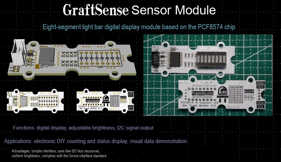
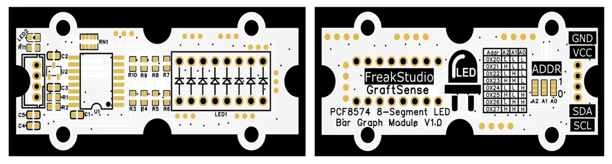
I. Module Introduction
8-segment bar digital tube module based on PCF8574 chip, with PCF8574T/TR IO expansion chip as the core, realizes the control of the 8-segment bar digital tube through the I2C interface, and only needs two communication pins to complete the driving. The module is equipped with chip address selection bits. Each I/O pin can sink a maximum current of about 10mA, which is suitable for the display expansion scenario of bar digital tubes in embedded devices, and provides a concise multi-segment bar display control solution for the system.
II. Introduction to Major Chips
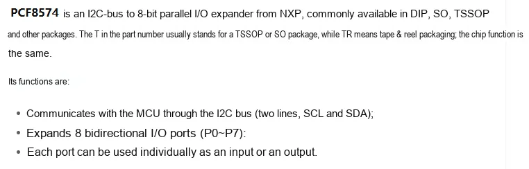
PCF8574DWR is an I²C bus expander chip that can expand the 2-wire I²C interface into an 8-bit parallel I/O port, requires no additional clock or control signals, and supports bidirectional data transmission. It is compatible with a wide supply voltage range of 2.5V to 6V, operates at a temperature range of -40°C to 85°C, features strong output drive capability (can directly drive LEDs), integrates a power-on reset circuit, and comes in a 16-pin SOIC package. With its compact size and high compatibility, it is widely used in scenarios requiring additional parallel interfaces such as microcontroller I/O port expansion, industrial control, and smart homes.
2.1 Chip Overview
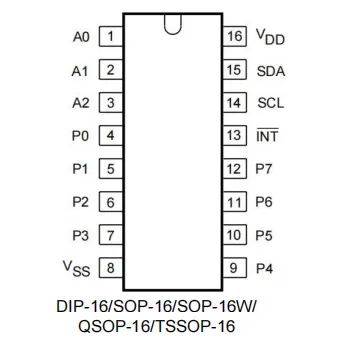
2.2 Pin Definition
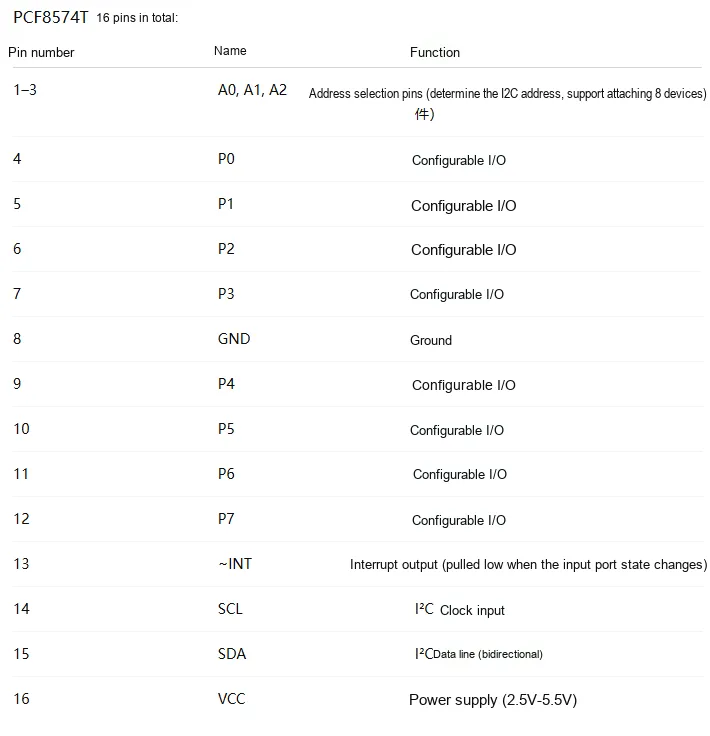
2.3 Functional Block Diagram
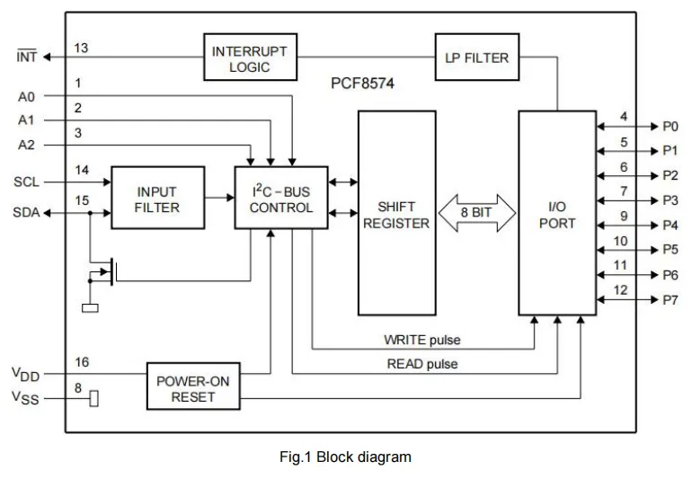
PCF8574DWR The functional block diagram is described as follows:
- Address and Interrupt Module
- A0, A1, A2: Address pins, which are used to set the address of the chip on the I²C bus to realize multi-device addressing.
- INTERRUPT LOGIC (Interrupt Logic): processes interrupt signals, and outputs interrupts to the outside through the INT pin, so as to implement trigger notification for external events.
- I²C Communication Module
- INPUT FILTER (Input Filtering): Filters the I²C signals input to the SCL and SDA pins to reduce noise interference.
- I²C-BUS CONTROL (I²C Bus Control): it serves as the core Control Unit for I²C communication, responsible for parsing I²C commands and coordinating data transmission timing.
- Data Processing and I/O Module
- SHIFT REGISTER: It realizes the serial-to-parallel conversion of data, and cooperates with I/O ports to complete data transmission and reception.
- I/O PORT (I/O Port, P0-P7): An 8-bit bidirectional I/O port that can function as an input or output interface for data interaction with external devices such as sensors and actuators.
- Power and Reset Module
- POWER-ON RESET (Power-On Reset): Provides a reset signal when the chip is powered on to initialize the internal state and ensure stable startup of the chip.
- Filtering and Time Series Module
- LP FILTER (Low-Pass Filter): Performs low-pass filtering on the signal to stabilize the internal signal quality.
- WRITE pulse, READ pulse: Read-write pulse generation module, which provides timing control for the read and write operations of shift registers and I/O ports.
Typical Scenario (Taking I/O Expansion as an Example):
- Data Writing: The main controller sends a write command via the I²C bus → the I²C-BUS CONTROL parses the command → the data is sent to the SHIFT REGISTER → and output to an external device through an I/O PORT (such as P0-P7).
- Data Reading and Interrupt: External device triggers input change of I/O PORT → INTERRUPT LOGIC generates INT interrupt → The main controller responds to the interrupt, reads the data of I/O PORT via I²C → completes the acquisition of external signals.
2.4 Performance Parameters
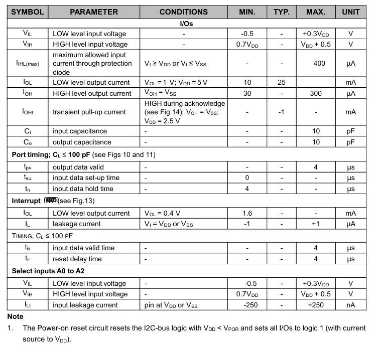
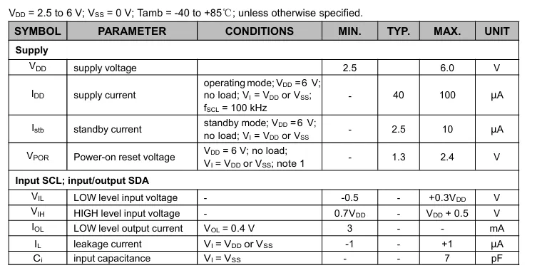
PCF8574DWR Some of the parameter descriptions are as follows:
- Power supply characteristics: Power supply voltage
- VDD supply voltage 2.5-6.0V
- IDD supply current Typical value: 40uA, maximum value: 100uA
- Power-on Reset Voltage Typical Value: 1.3V, Maximum Value: 2.4V
- Input/Output Characteristics (I/Os):
- Input level: low level V IL ≤ + 0.3 VDD, high level V IH ≥ 0.7 VDD; input leakage current I IH (max) is 400μA maximum.
- Output current: Low-level output current I OL, typical value 25 mA (V OL = 1 V, VDD = 5 V);
- Capacitance: Input and output capacitance C i, C o, maximum 10 pF.
- Port Timing: Output Data Valid Time t pv max. 4μs; Input Data Hold Time $t_{\text{h}}$ 4μs.
- Interrupt Characteristics: Low-level output current I OL min. 1.6 mA (V OL = 0.4 V); Leakage current I L -1 to + 1 μA; Input data valid time t pv, Reset delay time t r max. 4 μs.
- SCL/SDA Characteristics: Low-level output current I OL min. 3 mA (V OL = 0.4 V); Leakage current I L -1 to + 1 μA; Input capacitance C i max. 7 pF.
- Select Input (A0~A2): Low level V IL ≤ + 0.3 VDD, High level V IH ≥ 0.7 VDD; Input leakage current I LI: -250 ~ + 250 nA (pin connected to VDD or V SS).
2.5 Reference Circuit
None.
2.6 Chip Configuration
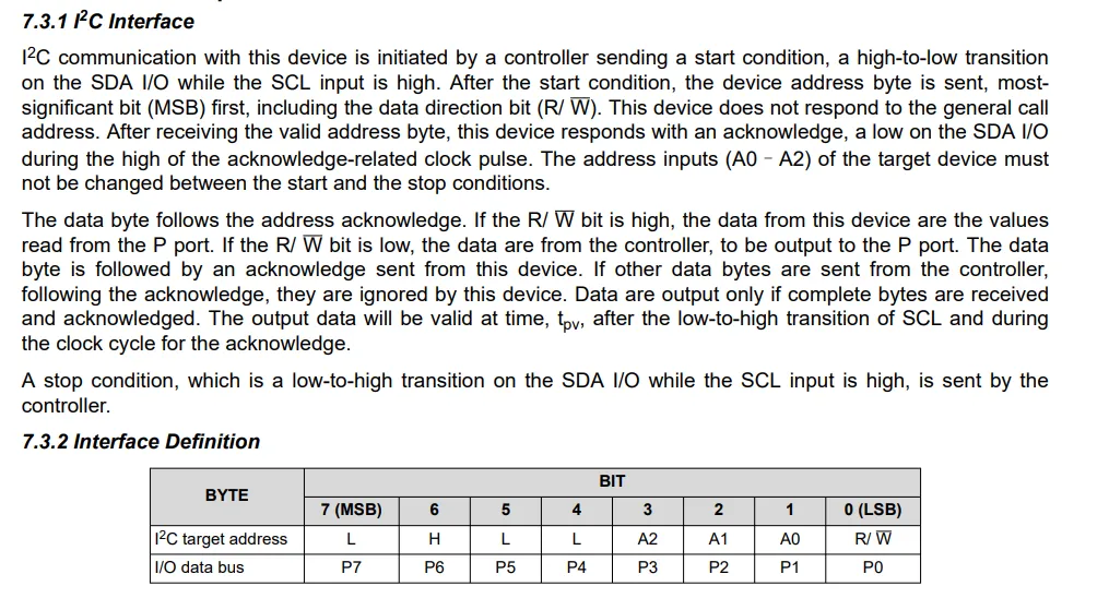
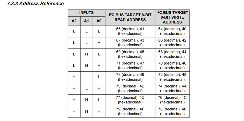
- Structure of I²C Target Address Byte
The I²C target address byte of the PCF8574DWR is 8 bits in total: the first 5 bits are fixed as "L, H, L, L"(i. e., binary 0100), the last 3 bits are determined by the levels of the chip's A2, A1, and A0 pins (L = low level, H = high level), and the final 1 bit is the read/write bit (R/ W, high for read, low for write).
- Correspondence Between I²C Target Addresses and Pins
The eight level combinations of A2, A1 and A0 correspond to different 8-bit read/write addresses:
When A2= A1= A0= L, the read address is decimal 65 (hexadecimal 41), and the write address is decimal 64 (hexadecimal 40);
When A2= A1= L and A0= H, the read address is 67 (43) and the write address is 66 (42);
By that analogy, each time the level of the A2/A1/A0 group is changed, the address increments according to the rule, and finally covers 8 different read and write address groups (for example, when A2= A1= A0= H, the read address is 79 (4F) and the write address is 78 (4E)).
- The levels of the address pins A0-A2 must not be modified during the START-STOP cycle of I²C communication; otherwise, address matching will fail.
2.7 Communication Interfaces and Related Protocols
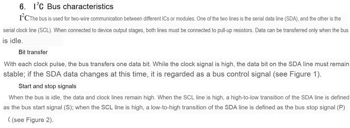
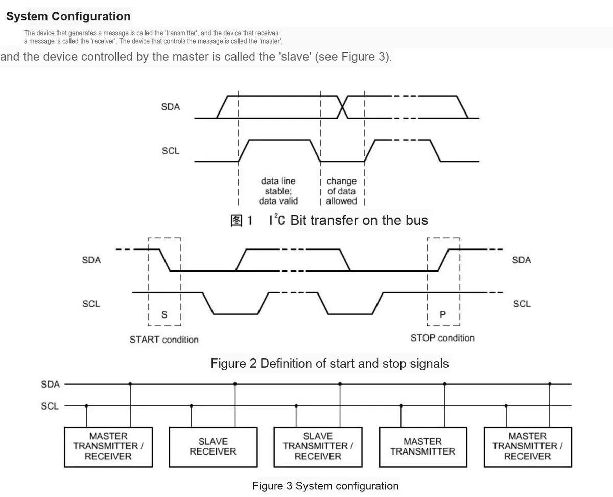
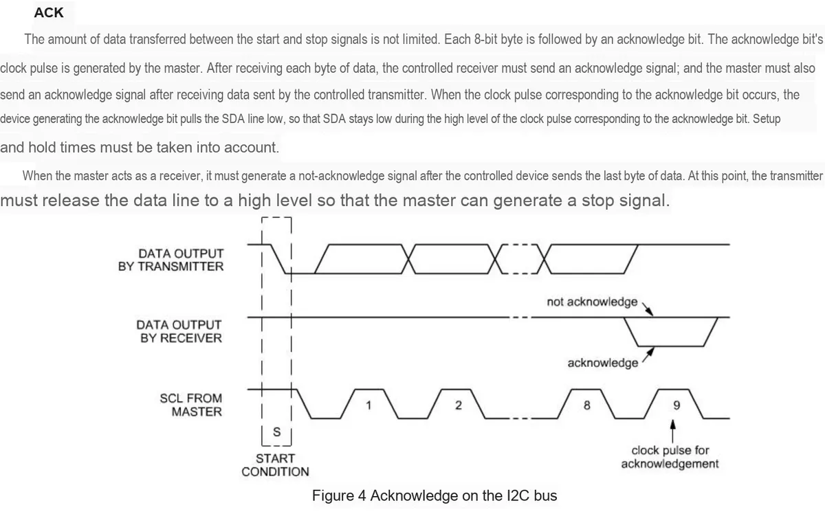
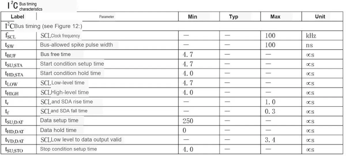
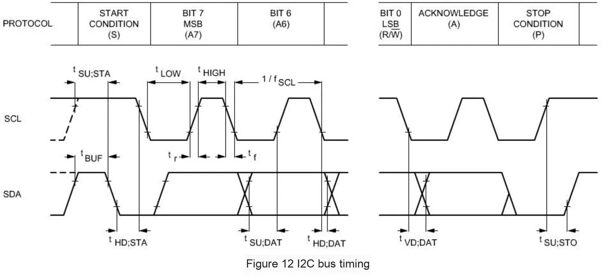
This chip adopts I2C communication interface.
2.7.1 I2C Communication Related
2.7.2 Quasi-bidirectional IO
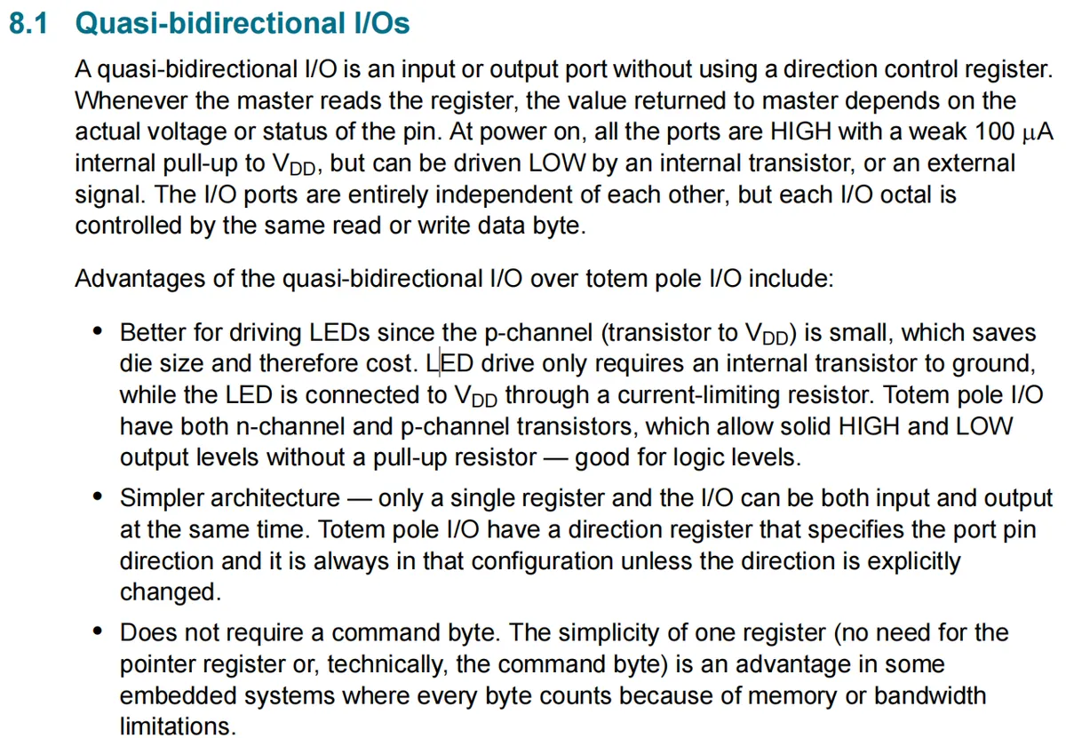
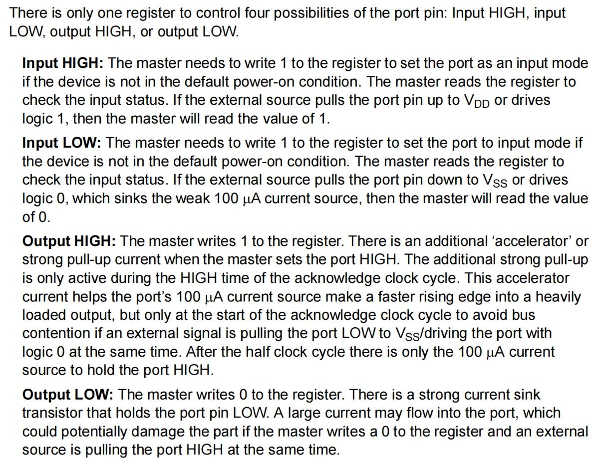
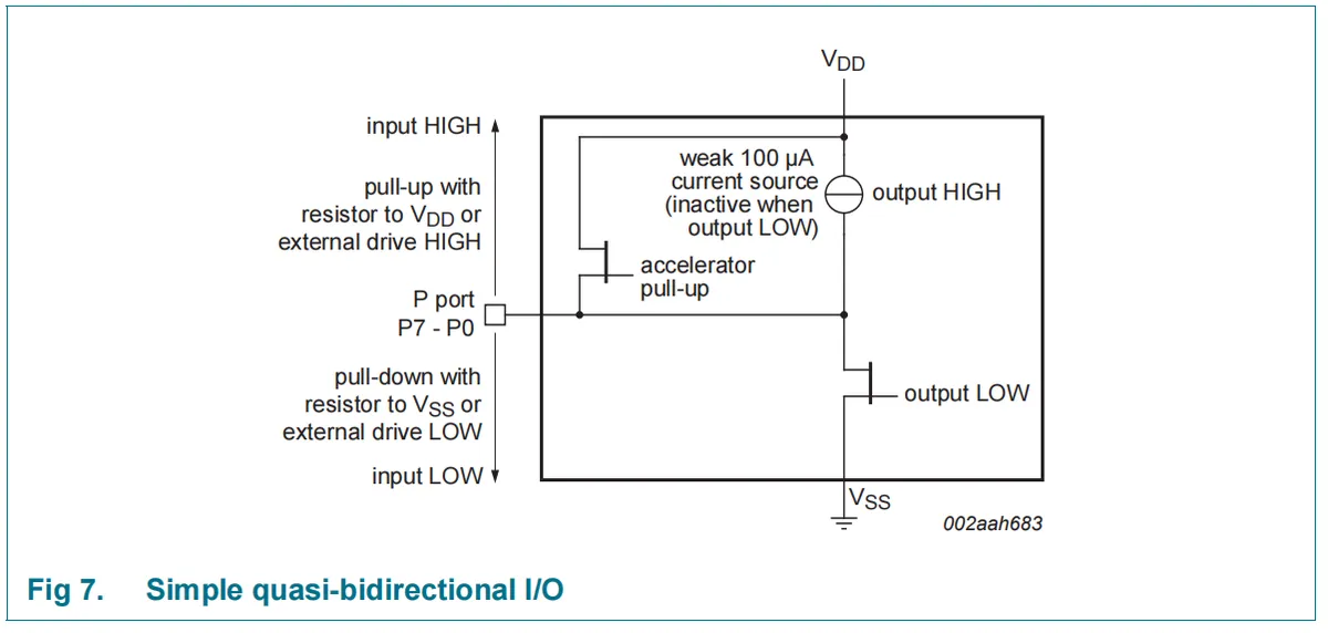
The PCF8574 adopts a quasi-bidirectional IO design, eliminating the need for a separate direction register, and can control four states of IO — input high, input low, output high, and output low — through a single register:
- By default upon power-up, all
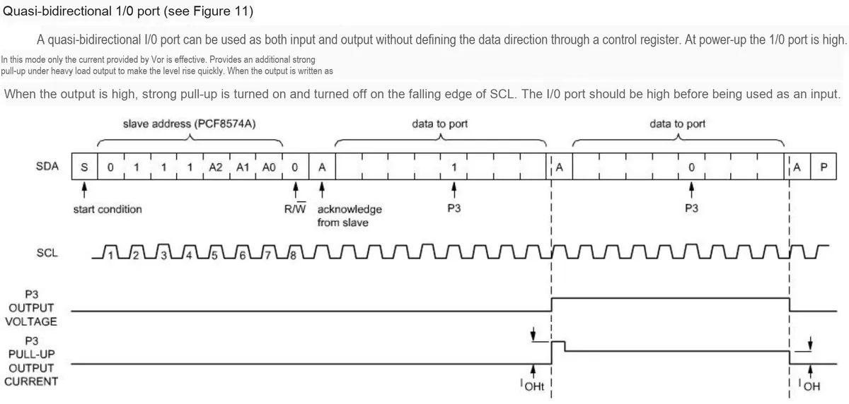
IOpins are at high level (with a 100μA weak pull-up); to configure a pin as input, write 1 to the corresponding register, and the host can read the external level by reading the register (reads 1 if the external pin is pulled high, reads 0 if pulled low); - Outputting a high level involves writing a 1 to the register; during the acknowledge clock cycle, an "accelerated pull-up" is triggered to make the auxiliary voltage rise rapidly, after which it is maintained solely by a weak pull-up.
- When outputting a low level, 0 is written to the register, and the level is pulled low by the strong current-sinking transistor; however, it is necessary to avoid external forced pulling-up of the IO which may cause device damage.
Compared with the totem-pole IO, this design has the advantages of being adaptable to LED driving, simple architecture, and no need for command bytes (saving memory/bandwidth), and its functions are implemented in the circuit by the cooperation of a weak pull-up current source, an accelerated pull-up transistor, and an output low-sink current transistor.
2.7.3 Writing to and Reading from Ports
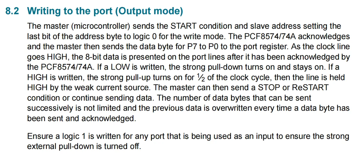
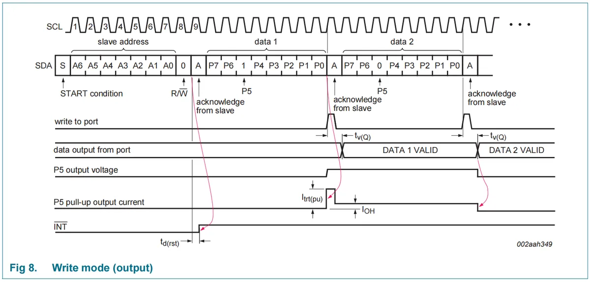

PCF8574 write port (output mode) follows the I²C communication process: the master first sends a START condition, then transmits the slave address (with the last bit set to 0 to indicate write mode); after the device acknowledges, the master sends 8-bit data from P7 to P0; once the clock line is pulled high and the device acknowledges, the data takes effect — when writing 0, the strong pull-down transistor remains continuously on; when writing 1, the strong pull-up only assists the voltage rise for half a clock cycle, and the high level is subsequently maintained by a 100μA weak pull-up.The master can continuously send multi-byte data (new data will overwrite old data), and finally send STOP / ReSTART to terminate;meanwhile, note that if the port is configured as an input, you must write 1 to it to turn off the strong pull-down transistor.
Combined with the Sequence Diagram and code examples, this process can be simplified as " START → Slave Address + Write → ACK → Data → ACK (repeatable) → STOP ", and the timing also reflects details such as the valid delay of data output and the dynamic change of pull-up current.
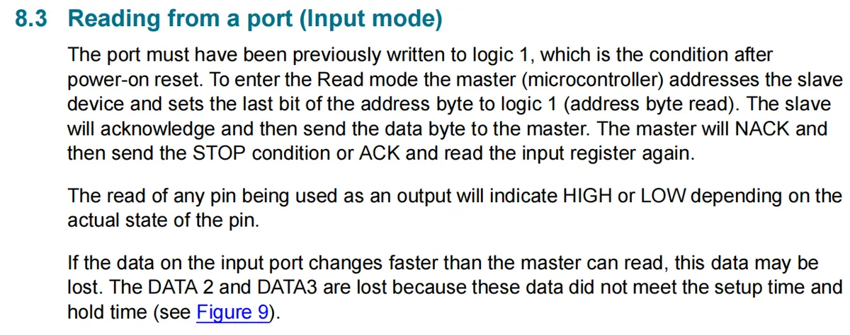
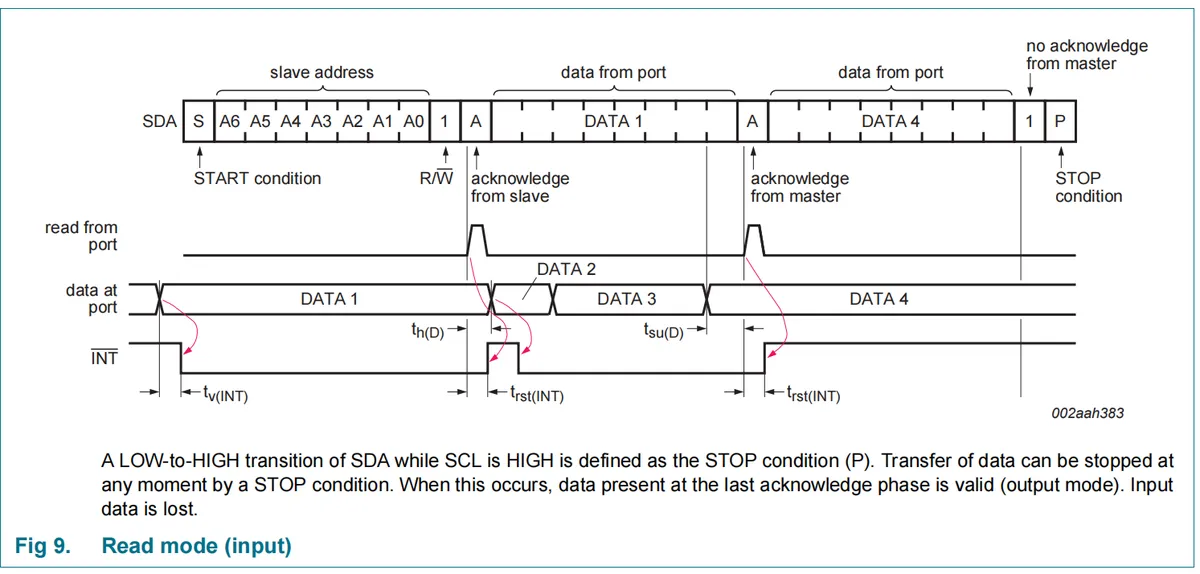

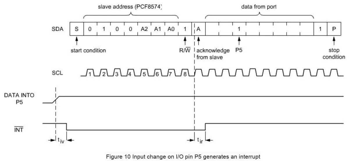
PCF8574 ’s port reading (input mode) is subject to a prerequisite: the port must be pre-written with 1 (this is the default state after power-on reset); its operation follows the I²C protocol: the master first sends a START condition, then transmits the slave address (with the last bit set to 1 to indicate read mode), and after the device acknowledges, it sends the port data byte to the master; the master can either send a NACK followed by a STOP to terminate the read, or send an ACK to continue reading the next byte.Note: Reading an output pin returns its actual logic level. If the input data changes faster than the host's reading pace, data will be lost due to failure to meet setup/hold time requirements. Combined with the Sequence Diagram and code examples, the process can be simplified as " START → Slave Address + Read → ACK → Data → ACK (repeatable) → Data → NACK → STOP ", and the timing also reflects the delay relationship between interrupts and data changes.
2.7.5 Power-on Reset
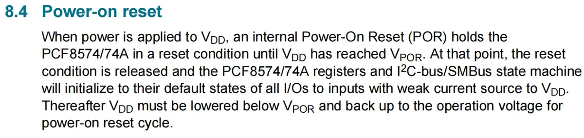
PCF8574 has the following power-on reset (POR) function logic: when VDD starts supplying power, the internal power-on reset circuit keeps the chip in a reset state until the VDD voltage reaches the power-on reset threshold VPOR; at this point the reset is released, and the chip's registers, I²C / SMBus finite-state machine will be initialized to the default state — all IO ports are configured as input mode with a weak current source pulled up to VDD. If you need to re-trigger the power-on reset subsequently, you must lower VDD below VPOR and then raise it back to the operating voltage to complete the reset cycle.
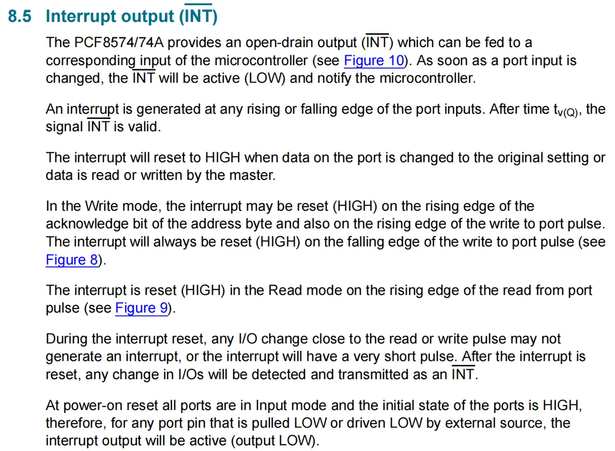
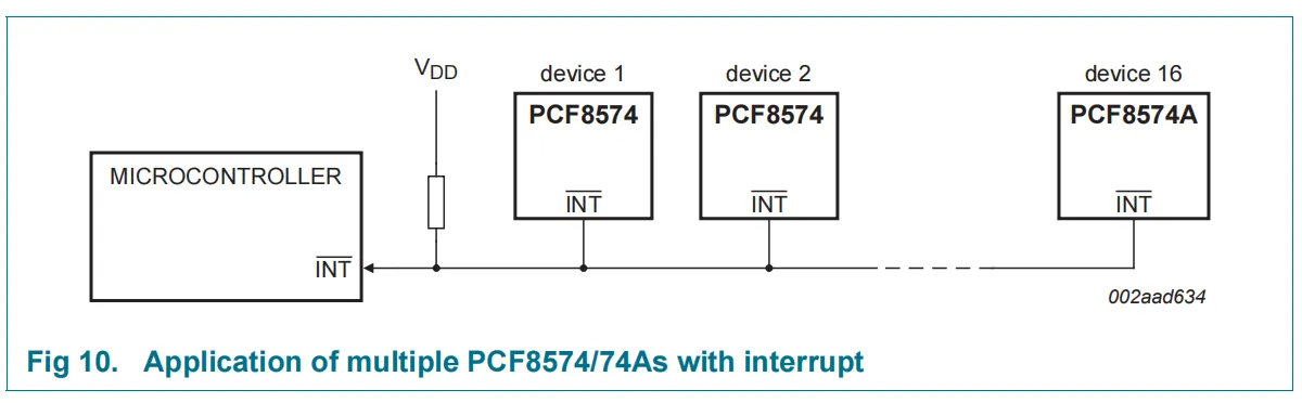
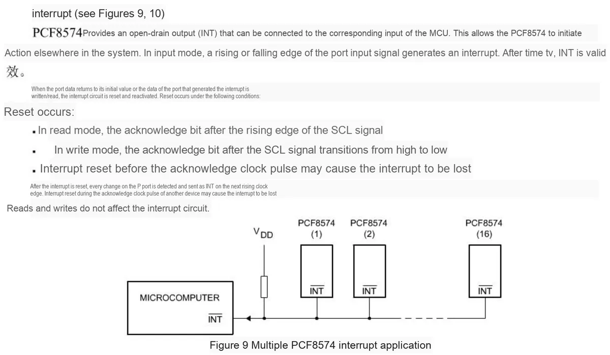
2.7.6 Interrupt Function
2.8 PCB Routing Precautions
None.
III. Circuit Engineering
3.1 Circuit Source Engineering
To obtain the source project of the circuit, please follow the official account [Freak Embedded]
3.2 Module Usage Instructions
SCH_Schematic1_8-Segment Light Bar Display Module Based on PCF8574 Chip-V1.0.0_2025-11-17.pdf 2.2 MB
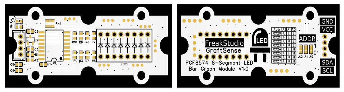
This module provides an I2C communication interface: it supports the standard I2C communication rate (100kHz), and can flexibly configure 8 types of A0, A1, A2 address selection bits to configure 0X20 - 0X27 and other I2C device addresses. It is compatible with 3.3V/5V logic levels, and can stably implement single-byte write of 8-bit data to control the on-off state of the 8-segment bar nixie tube (each bit of data corresponds to the on/off of one light bar). It is suitable for scenarios such as status indication of embedded devices, bar visualization of sensor values, and interactive display for maker projects, providing the system with simple and efficient multi-segment light bar display control capability.
3.3 Application Experiment
Here, we use the GraftPort-RP2040 development board for testing, and connect the 8-segment bar digital tube module based on the PCF8574 chip to communicate with the main controller via the I2C interface.
Here, we first use the HY2.0-4P cable to connect the module to the GraftPort-RP2040 development board's I2C0 interface:
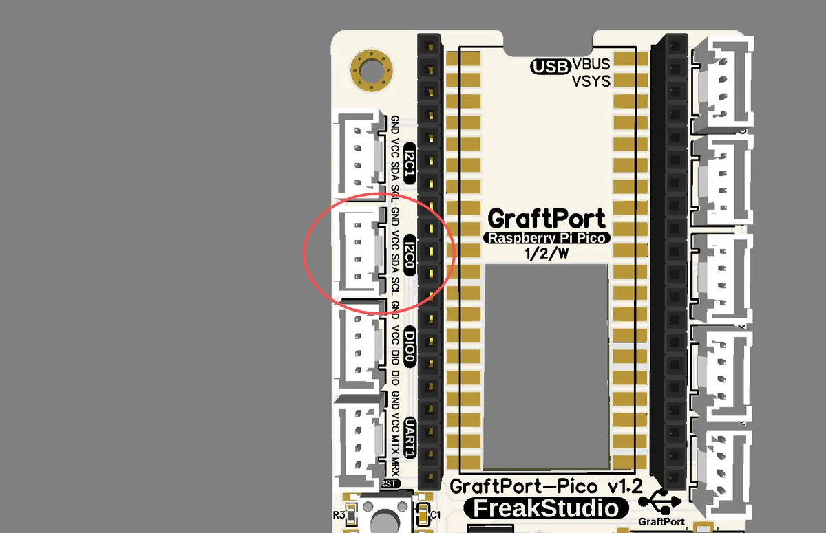
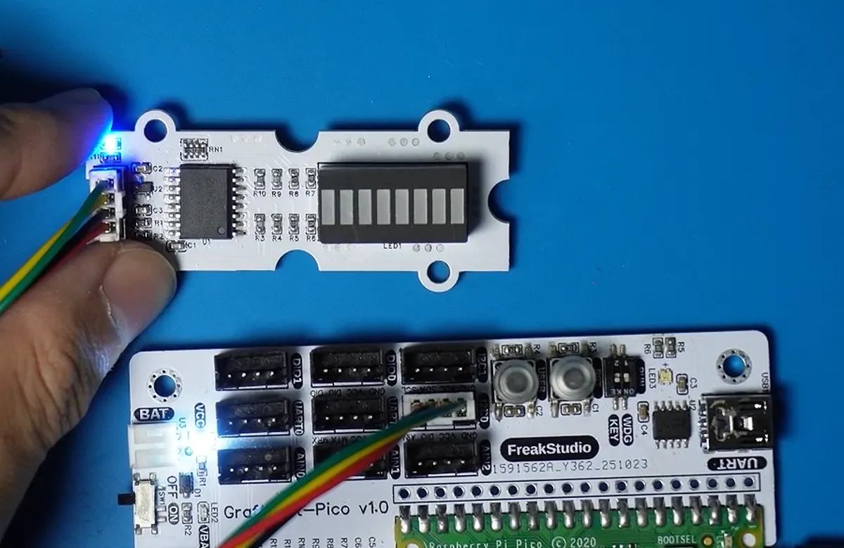
The module connections are shown in the following table:
Development Board Pins | Module Pins | Description |
Pin 4 |
| I2C data transmission line, corresponding to |
Pin 5 |
| I2C clock signal line, corresponding to |
Here, we need to search for the relevant driver packages on uPyPI: https://upypi.net/zh/
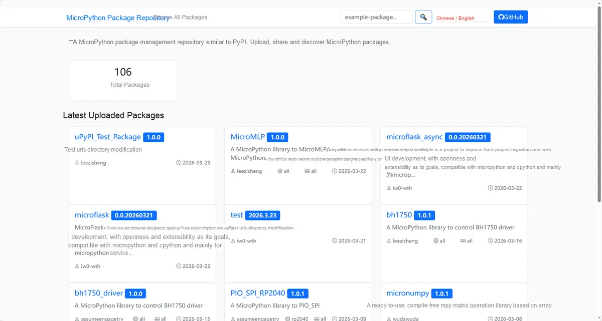
Enter pcf8574_led_driver to search, and the following will be displayed:

Click to copy the local installation command:
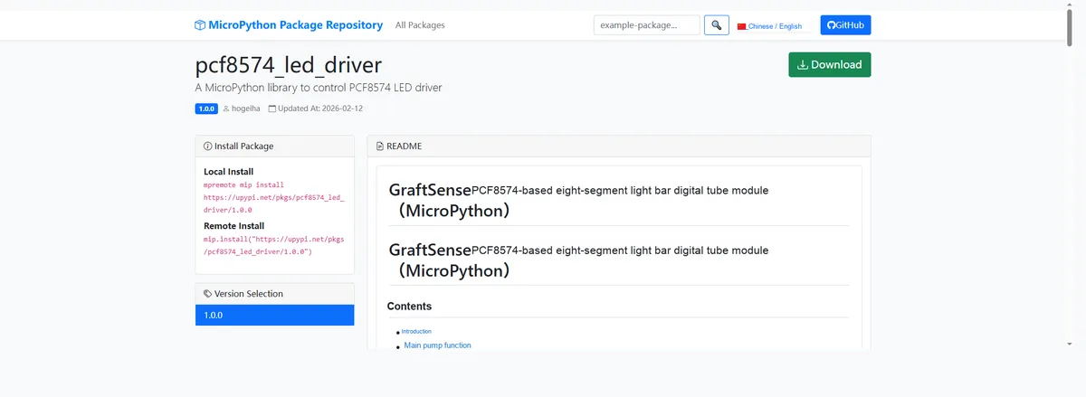
Here, we can use the mip tool to import module driver library code. The following are the usage commands for the mpremote tool:
mpremote mip install github:FreakStudioCN/GraftSense-Drivers-MicroPython/lighting/pcf8574_led_driverAfter importing the 8-segment bar digital tube module based on PCF8574 chip - MicroPython driver code, copy the following main.py code into our project:
# Python env   : MicroPython v1.23.0
# -*- coding: utf-8 -*-
# @Time    : 2025/09/08 10:00
# @Author  : 侯钧瀚
# @File    : main.py
# @Description : Eight-segment light bar digital tube module based on the PCF8574 chip

# ======================================== Import Modules =========================================

from machine import I2C, Pin
#Import the pcf8574 module
from pcf8574 import PCF8574
#Import the eight-segment light bar digital tube module based on the PCF8574 chip
from led_bar import LEDBar
#Time-related module
import time

# ======================================== Global Variables ============================================

# ======================================== Functions ============================================

# ======================================== Custom Classes ============================================

# ======================================== Initialization ==========================================

# Power-on delay of 3 s
time.sleep(3)
# Print debug message
print("FreakStudio: Test PCF8574 Eight-Segment LED Display Module ")

i2c = I2C(id=0, sda=Pin(4), scl=Pin(5), freq=100000)
# Start scanning for devices on the I2C bus and return a list of slave addresses
devices_list = i2c.scan()
print('START I2C SCANNER')

# If devices_list is empty, no device is connected to the I2C bus
if len(devices_list) == 0:
    print("No i2c device !")
# If not empty, print the slave device addresses
else:
    print('i2c devices found:', len(devices_list))
    # Iterate over the slave device address list
    for device in devices_list:
        # Check whether the device address is the PCF8575 address
        if device >= 0x20 and device <= 0x27:
            print("I2C hexadecimal address: ", hex(device))

# Initialize PCF8574, assuming address 0x20
pcf = PCF8574(i2c, address=device)
# Create an LEDBar instance
ledbar = LEDBar(pcf)

# ========================================  Main Program  ===========================================

# 1. Turn on a single LED (turn on the 3rd LED)
ledbar.set_led(2, True)
time.sleep(1)

# 2. Turn off a single LED (turn off the 3rd LED)
ledbar.set_led(2, False)
time.sleep(1)

# 3. Set all LEDs (e.g., turn on the first 4)
ledbar.set_all(0b00001111)
time.sleep(1)

# 4. Display level (e.g., turn on the first 6 LEDs)
ledbar.display_level(6)
time.sleep(1)

# 5. Running light effect
for i in range(8):
    ledbar.set_all(1 << i)
    time.sleep(0.2)

# 6. Turn all off
ledbar.clear()
To flash the code, open a terminal and use the mpremote tool to connect to the main controller; the output is as follows:
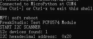
It can be seen that the lights will illuminate sequentially in accordance with the process specified in the code.
IV. Drivers
pcf8574_led_driver.zip 11 KB
5. BOM & Recommended Alternative Parts
None.
VI. Revision History
Document Version | Date of Modification | Modifier | Modified Content |
v1.0 | 2025-11-17 | Ling Gaoxing | Initialize the document |
v1.1 | 2025-12-29 | Li Zisheng | Added application experiments and production files |
v1.2 | 2025-12-31 | Xin Ruili | Create an open version of the document based on the internal document version v1.1. |
v1.3 | 2026-03-29 | Xin Ruili | Modified the application experiment section. |
VII. Relevant Materials
7.1 Chip Datasheet
PCF8574 Manual.pdf 3.4 MB
7.2 Unique Icons for PCB Silkscreen