Contents
- I. Module Introduction
- II. Introduction to Main Chips
- 2.1 Chip Overview
- 2.2 Pin Definition
- 2.3 Functional Block Diagram
- 2.4 Performance Parameters
- 2.5 Reference Circuit
- 2.6 Chip Configuration
- 2.7 Communication Interfaces and Related Protocols
- 2.8 PCB Routing Precautions
- III. Circuit Engineering
- 3.1 Circuit Source Engineering
- 3.2 Module Usage Instructions
- 3.3 Application Experiment
- IV. Drivers
- 5. BOM & Recommended Alternative Parts
- VI. Revision History
- VII. Relevant Materials
- 7.1 Chip Datasheet
- 7.2 Unique Icons for PCB Silkscreen
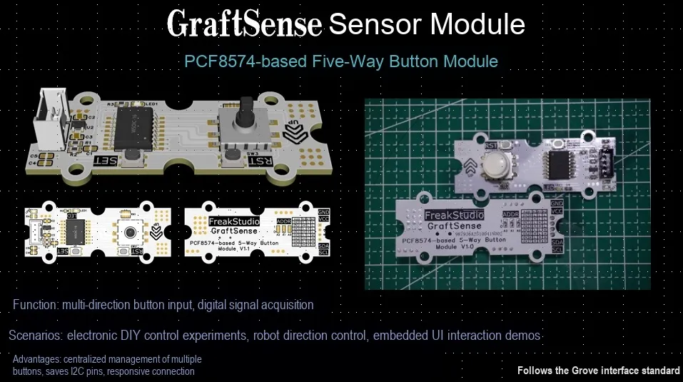
I. Module Introduction
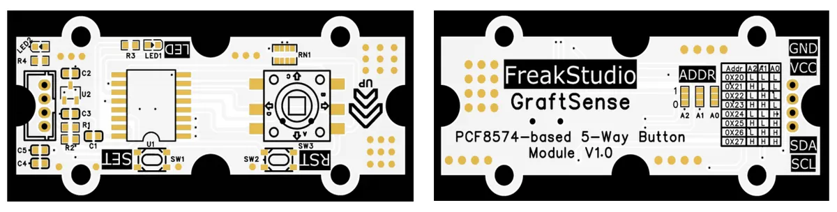
5-direction key module based on PCF8574, with the PCF8574DWR chip as the core, connects to the microcontroller via the I2C interface (communication voltage level: 3.3V). Equipped with a 5-direction key (with independent contacts for center, up, down, left and right), tact switches and LED indicators, the module also features chip address selection, MCU interface, power filtering and indicator lights, which is suitable for key input expansion scenarios of embedded devices and provides a flexible human-computer interaction key control solution for the system.
II. Introduction to Main Chips
PCF8574DWR is an I²C bus expansion chip that can extend the 2-wire I²C interface to an 8-bit parallel I/O port, supporting bidirectional data transmission without requiring additional clock or control signals. It is compatible with a wide supply voltage range of 2.5V to 6V, operates at a temperature range of -40°C to 85°C, features strong output drive capability (can directly drive LED s), incorporates a built-in power-on reset circuit, and comes in a 16-pin SOIC package. With compact size and high compatibility, it is widely used in scenarios requiring additional parallel interfaces such as microcontroller I/O port expansion, industrial control, and smart homes.
A five-way key is a common input device, typically used in the control interfaces of electronic products such as remote controls, game controllers and mobile devices. It contains five internal contacts: a common contact at the center, with multiple fixed contacts distributed around it. Its operating principle relies on the movable contact spring to connect with the common contact and the surrounding fixed contacts, so as to realize the switching of multiple states. When the operating lever is moved, the movable contact spring comes into contact with the corresponding contact, thereby forming a circuit connection.
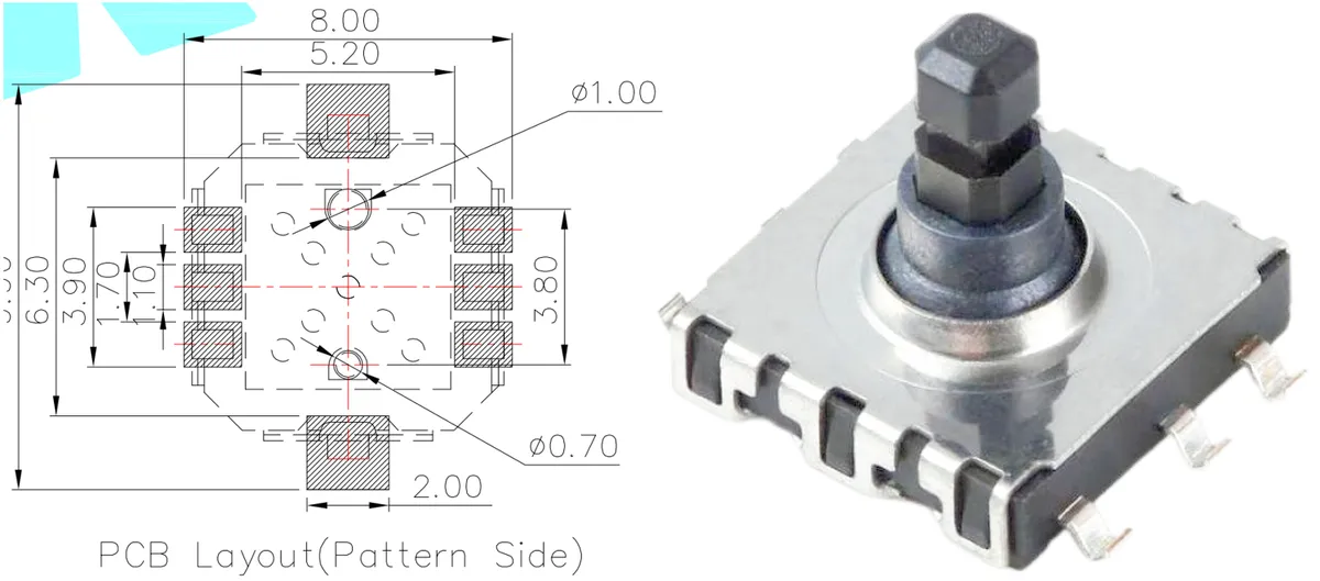
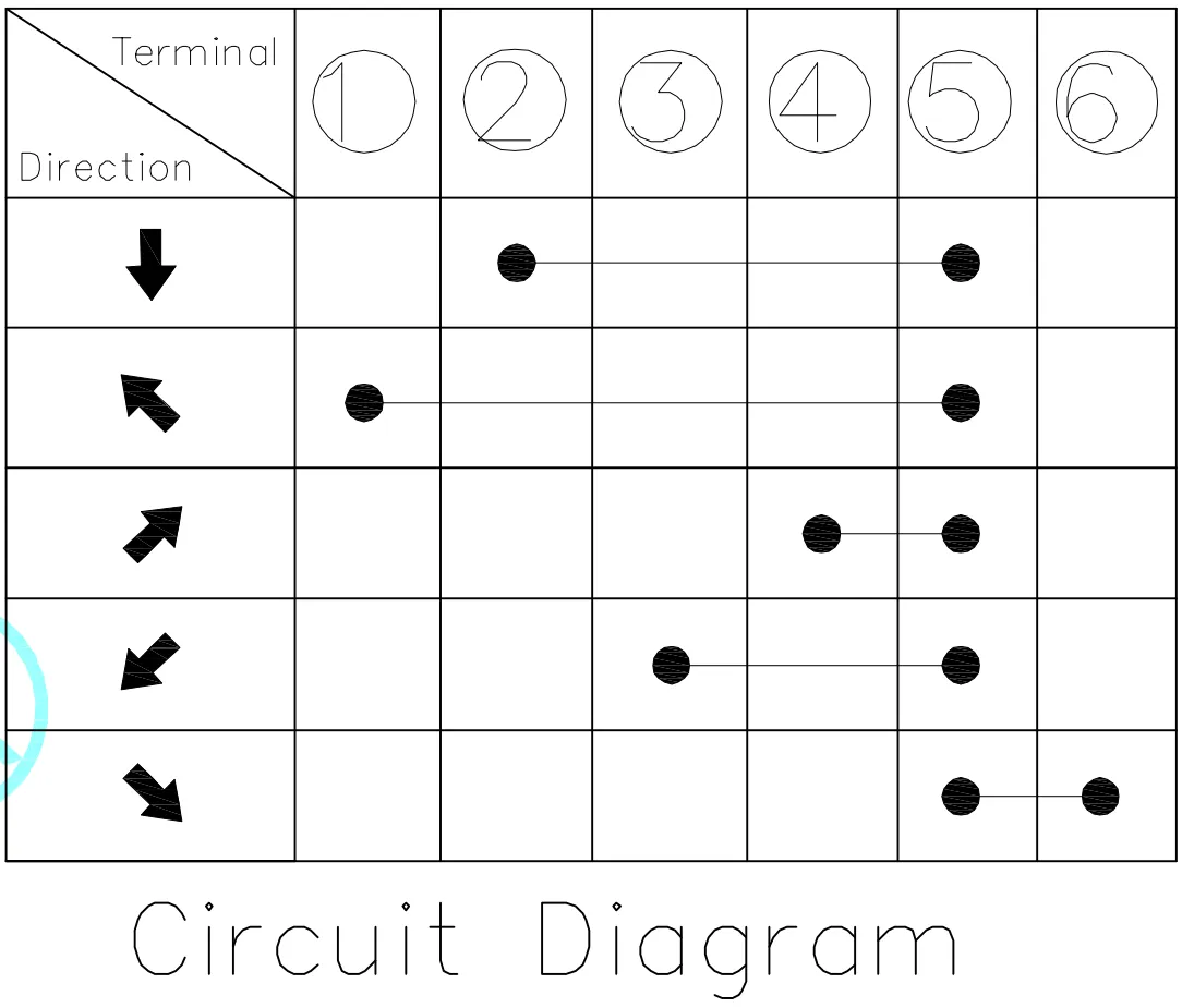
A 5-way key looks like a single key, but it actually contains five distinct key states. By pressing it in different directions, users can switch between multiple functions. Here, we connect the common contact (COM terminal) of the 5-way key to the + 5V power supply. When none of the keys is pressed, the voltage measured at any key is 0V, because all contacts are in an open circuit state and no current flows; when any key is pressed, the movable contact spring of that key will connect with the common contact to form a closed circuit, and the voltage of the corresponding key measured at this time will rise to the supply voltage (5V).
2.1 Chip Overview
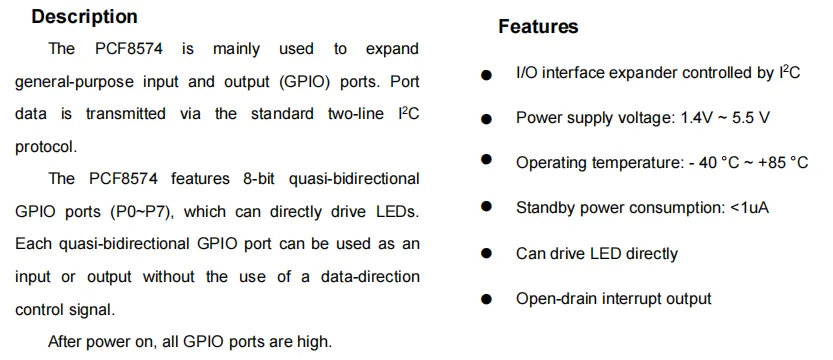
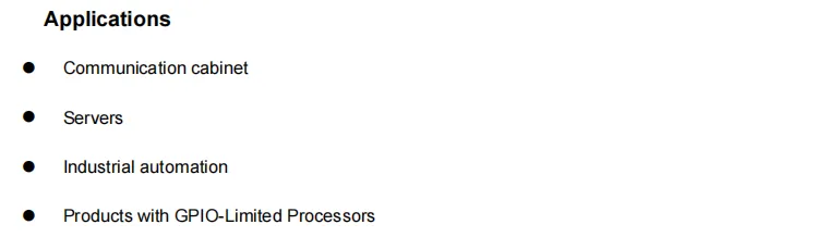
PCF8574 is a chip that implements general-purpose I²C protocol-based I/O port expansion, equipped with 8-bit quasi-bidirectional GPIO ports (P0 to P7), which can be flexibly used as input/output without direction control signals. After power-on, the GPIO pins default to high level, can directly drive LED s, and also support open-drain interrupt output;It is compatible with 1.4V~5.5V power supply, operates within the temperature range of -40℃~+ 85℃, and has a standby power consumption of <1μA. It is mainly applied to communication cabinets, servers, industrial automation and GPIO processor devices with insufficient resources to meet the I/O port expansion requirements.
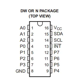
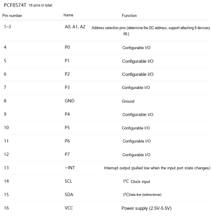
2.2 Pin Definition
2.3 Functional Block Diagram
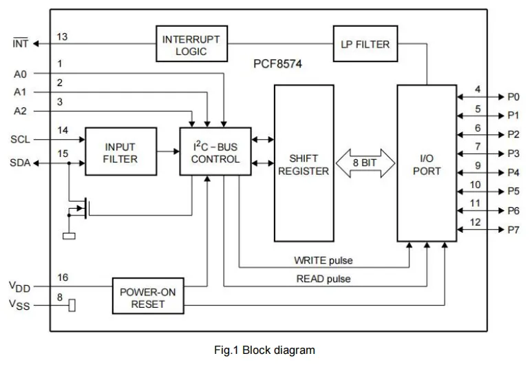
PCF8574DWR The functional block diagram is described as follows:
- Address and Interrupt Module
- A0, A1, A2: Address pins, which are used to set the address of the chip on the I²C bus to realize multi-device addressing.
- INTERRUPT LOGIC (Interrupt Logic): processes interrupt signals, and outputs interrupts to the outside through the INT pin, so as to implement trigger notification for external events.
- I²C Communication Module
- INPUT FILTER (Input Filtering): Filters the I²C signals input to the SCL and SDA pins to reduce noise interference.
- I²C-BUS CONTROL (I²C Bus Control): it serves as the core Control Unit for I²C communication, responsible for parsing I²C commands and coordinating data transmission timing.
- Data Processing and I/O Module
- SHIFT REGISTER: It realizes the serial-to-parallel conversion of data, and cooperates with I/O ports to complete data transmission and reception.
- I/O PORT (I/O Port, P0-P7): An 8-bit bidirectional I/O port that can function as an input or output interface for data interaction with external devices such as sensors and actuators.
- Power and Reset Module
- POWER-ON RESET (Power-On Reset): Provides a reset signal when the chip is powered on to initialize the internal state and ensure stable startup of the chip.
- Filtering and Time Series Module
- LP FILTER (Low-Pass Filter): Performs low-pass filtering on the signal to stabilize the internal signal quality.
- WRITE pulse, READ pulse: Read-write pulse generation module, which provides timing control for the read and write operations of shift registers and I/O ports.
Typical Scenario (Taking I/O Expansion as an Example):
- Data Writing: The main controller sends a write command via the I²C bus → the I²C-BUS CONTROL parses the command → the data is sent to the SHIFT REGISTER → and output to an external device through an I/O PORT (such as P0-P7).
- Data Reading and Interrupt: External device triggers input change of I/O PORT → INTERRUPT LOGIC generates INT interrupt → The main controller responds to the interrupt, reads the data of I/O PORT via I²C → completes the acquisition of external signals.
2.4 Performance Parameters
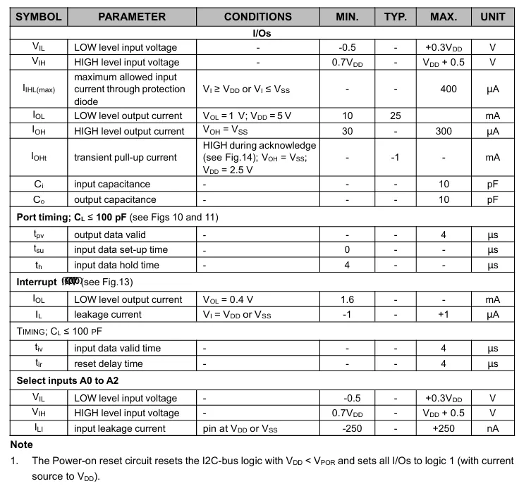
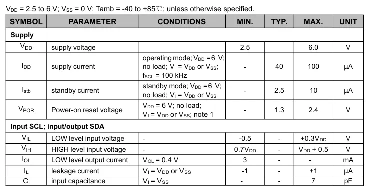
PCF8574DWR Some of the parameter descriptions are as follows:
- Power supply characteristics: Power supply voltage
- VDD supply voltage 2.5-6.0V
- IDD supply current Typical value: 40uA, maximum value: 100uA
- Power-on Reset Voltage Typical Value: 1.3V, Maximum Value: 2.4V
- Input/Output Characteristics (I/Os):
- Input level: low level V IL ≤ + 0.3 VDD, high level V IH ≥ 0.7 VDD; input leakage current I IH (max) is 400μA maximum.
- Output current: Low-level output current I OL, typical value 25 mA (V OL = 1 V, VDD = 5 V);
- Capacitance: Input and output capacitance C i, C o, maximum 10 pF.
- Port Timing: Output Data Valid Time t pv max. 4μs; Input Data Hold Time $t_{\text{h}}$ 4μs.
- Interrupt Characteristics: Low-level output current I OL min. 1.6 mA (V OL = 0.4 V); Leakage current I L -1 to + 1 μA; Input data valid time t pv, Reset delay time t r max. 4 μs.
- SCL/SDA Characteristics: Low-level output current I OL min. 3 mA (V OL = 0.4 V); Leakage current I L -1 to + 1 μA; Input capacitance C i max. 7 pF.
- Select Input (A0~A2): Low level V IL ≤ + 0.3 VDD, High level V IH ≥ 0.7 VDD; Input leakage current I LI: -250 ~ + 250 nA (pin connected to VDD or V SS).
2.5 Reference Circuit
None.
2.6 Chip Configuration
None.
2.7 Communication Interfaces and Related Protocols
2.7.1 I²C Bus Features
I²C bus is used for bidirectional two-wire communication between different ICs or modules. The two wires are the Serial Data Line (SDA) and the Serial Clock Line (SCL) respectively. When connected to the output stage of a device, both wires must be connected to the positive power supply via pull-up resistors. Data transmission can only be initiated when the bus is idle.
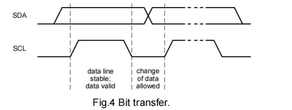
2.7.2 Bit Transmission
One bit of data is transmitted per clock pulse. During the high level of the clock pulse, SDA line must remain stable, as any change on the data line at this time will be interpreted as a control signal.
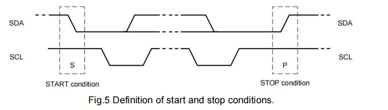
2.7.3 Start and Stop Conditions
When the bus is idle, both the data line and the clock line remain at a high level. When the clock is at a high level, the transition of the data line from high to low is defined as a start condition (S). When the clock is at a high level, the transition of the data line from low to high is defined as a stop condition (P).
2.7.4 System Configuration
The device that generates messages is the "transmitter", and the device that receives messages is the "receiver". The device that controls messages is the "master device", and the device controlled by the master device is the "slave device"(see the figure below).
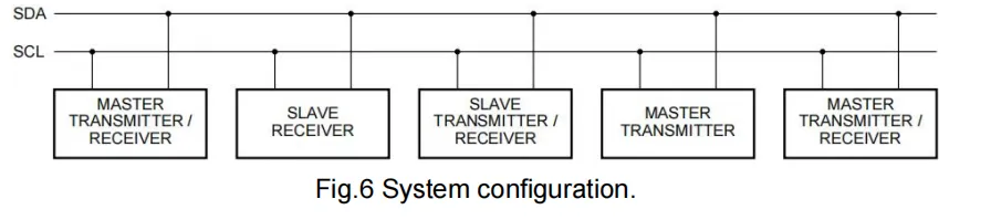
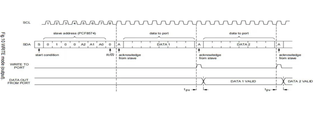
Between the start condition and the stop condition, there is no limit on the number of data bytes transmitted from the transmitter to the receiver. Each 8-bit byte is followed by 1 acknowledge bit. The acknowledge bit is a high level driven onto the bus by the transmitter, while the master device generates an additional acknowledge-related clock pulse.
The addressed slave receiver must generate an acknowledge after the reception of each byte. Also a master must generate an acknowledge after the reception of each byte that has been clocked out by the slave transmitter. The device that acknowledges must pull down the SDA line during the acknowledge clock pulse, so that the SDA line is stable low during the HIGH period of the acknowledge related clock pulse, taking into account the setup and hold times.
The master receiver must signal the end of data to the transmitter by not generating an acknowledge for the last byte of the clock output from the slave device. In this case, the transmitter must hold the data line high to allow the master to generate a stop condition.
Write Mode Sequence Diagram:
Read Mode Sequence Diagram:
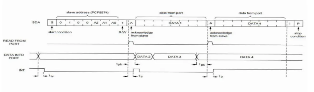
When SCL is at a high level, a high-to-low transition of SDA is defined as the stop condition (P). Data transmission can be stopped at any time via the stop condition. When this occurs, the valid data from the last acknowledge phase (in output mode) remains valid, while the input data will be lost.
2.7.5 I²C Bus Timing Characteristics
| Symbol | Parameter | Min | Typ | Max | Unit |
| fSCL | SCL clock frequency | - | - | 100 | kHz |
| tSW | Tolerable spike width on the bus | - | - | 100 | ns |
| tBUF | Bus free time | 4.7 | - | - | μs |
| tSU:STA | Start condition setup time | 4.7 | - | - | μs |
| tHD:STA | Start condition hold time | 4 | - | - | μs |
| tLOW | SCL low time | 4.7 | - | - | μs |
| tHIGH | SCL high time | 4 | - | - | μs |
| tr | SCL and SDA rise time | - | - | 1 | μs |
| tf | SCL and SDA fall time | - | - | 0.3 | μs |
| tSU:DAT | Data setup time | 250 | - | - | ns |
| tHD:DAT | Data hold time | 0 | - | - | ns |
| tVD:DAT | SCL low to data output valid time | - | - | 3.4 | μs |
| tSU:STO | Stop condition setup time | 4 | - | - | μs |
Note: All timing values are valid within the range of operating power supply voltage and ambient temperature, and refer to V SS to V DD for the input voltage swing, corresponding to V IL and V IH.
The Sequence Diagram of the IIC bus is as follows:
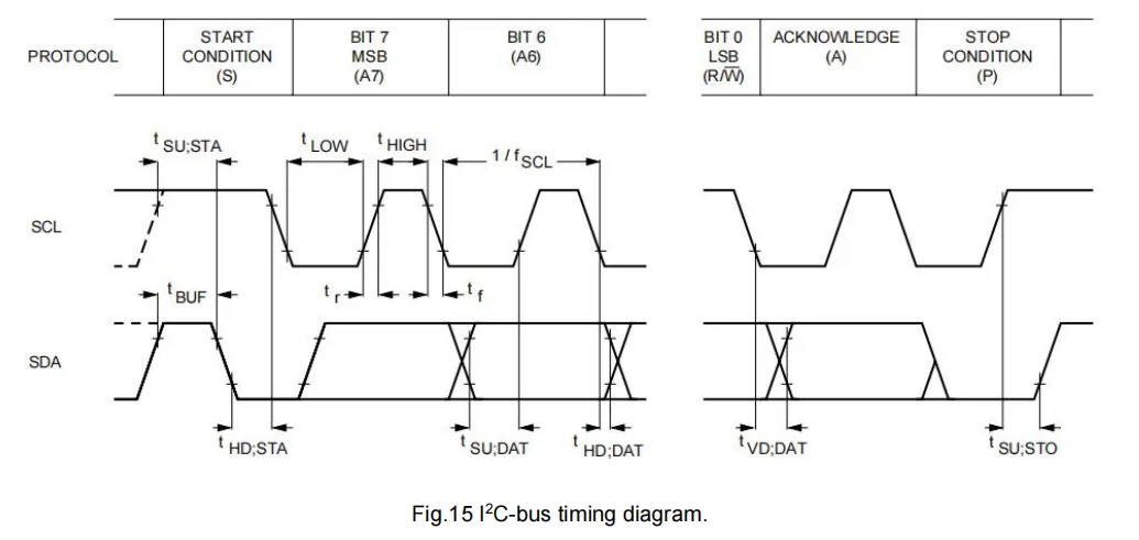
2.8 PCB Routing Precautions
None.
III. Circuit Engineering
3.1 Circuit Source Engineering
To obtain the source project of the circuit, please follow the official account [Freak Embedded]
3.2 Module Usage Instructions
SCH_Schematic1_0.96-inch SSD1306-OLED Module-V1.1_2025-11-13.pdf 1.9 MB
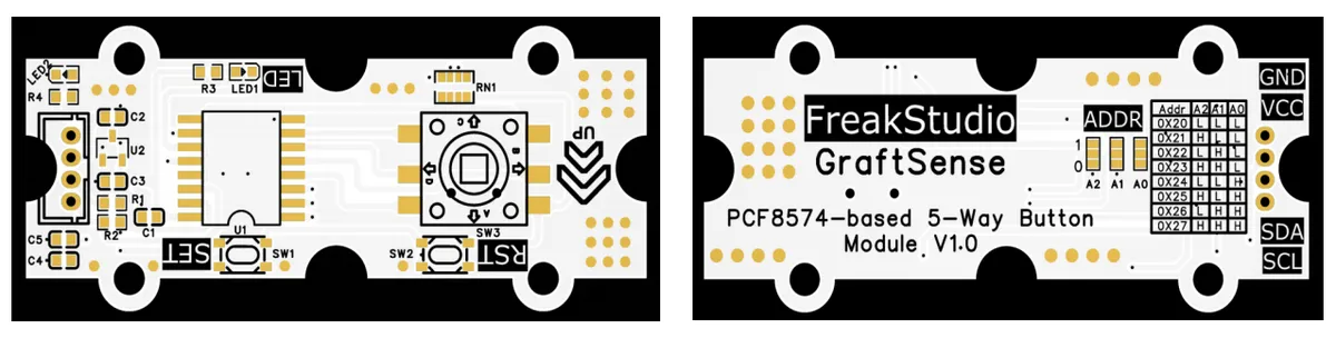
This module provides an I2C pins. It is compatible with 3.3V communication level, and can stably transmit the input signals of the 5-way buttons (center, up, down, left, right) and tact switches. It is suitable for scenarios such as human-computer interaction button expansion for embedded devices and button input control for maker projects, providing the system with flexible I2C communication rates, and can flexibly configure 8 types of I2C device addresses ranging from 0x20 to 0x27 via the A0, A1, and A2 pins. It is compatible with 3.3V communication level, and can stably transmit the input signals of the 5-way buttons (center, up, down, left, right) and tact switches. It is suitable for scenarios such as human-computer interaction button expansion for embedded devices and button input control for maker projects, providing the system with flexible I/O extended button interaction capabilities.
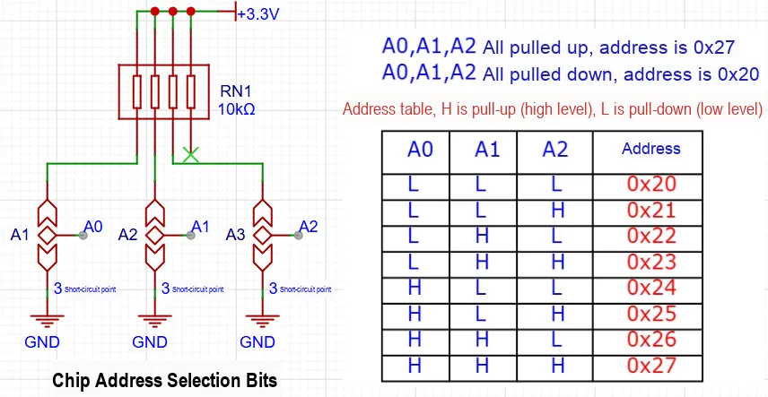
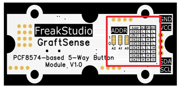
PCF8574DWR 's IIC address can be selected via the 3 short-circuit points on the back of the physical device, and the address truth table is shown in the following figure.
3.3 Application Experiment
Here, we use the GraftPort-RP2040 development board for testing, and connect the 5-way button module based on PCF8574 to communicate with the main controller via the I2C interface.
Here, we need to set the address bits in advance by soldering two short-circuit points:
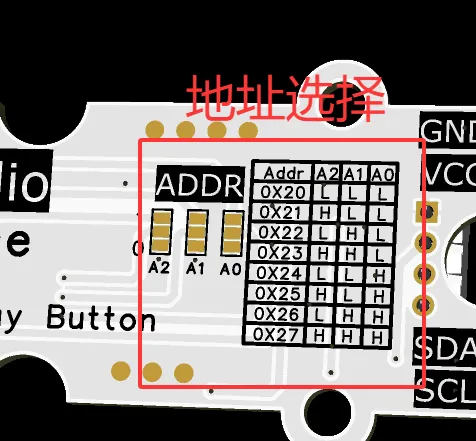
Here, we first use the HY2.0-4P cable to connect the module to the GraftPort-RP2040 development board's I2C0 interface:
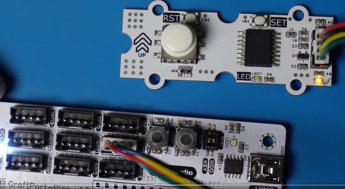
The module connections are shown in the following table:
Development Board Pins | Module Pins | Description |
Pin 4 |
|
|
Pin 5 |
|
|
Here, we need to search for the relevant driver packages on uPyPI: https://upypi.net/zh/
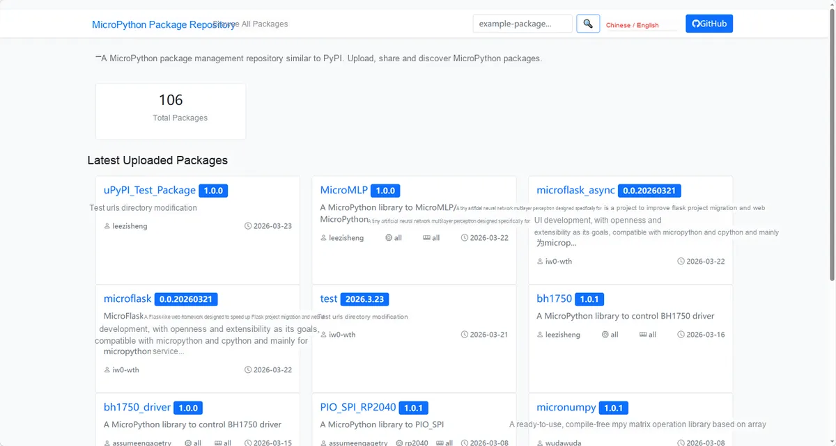
Enter pcf8574keys_driver to search, and the following will be displayed:
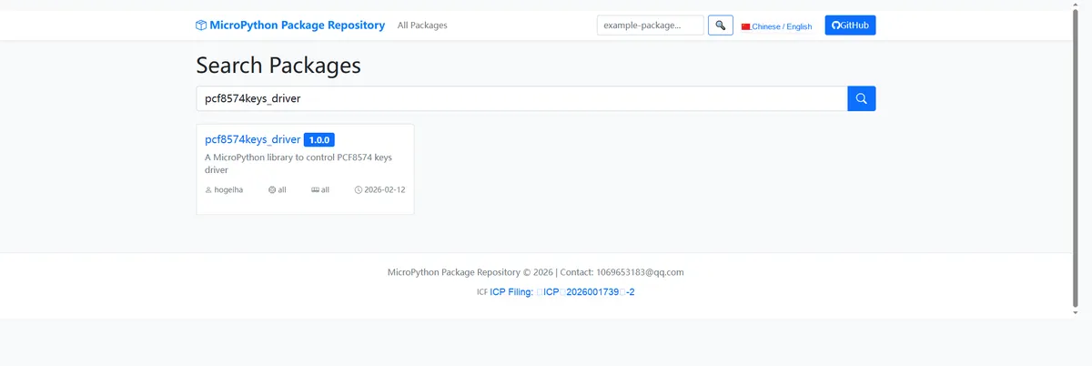
Click to copy the local installation command:
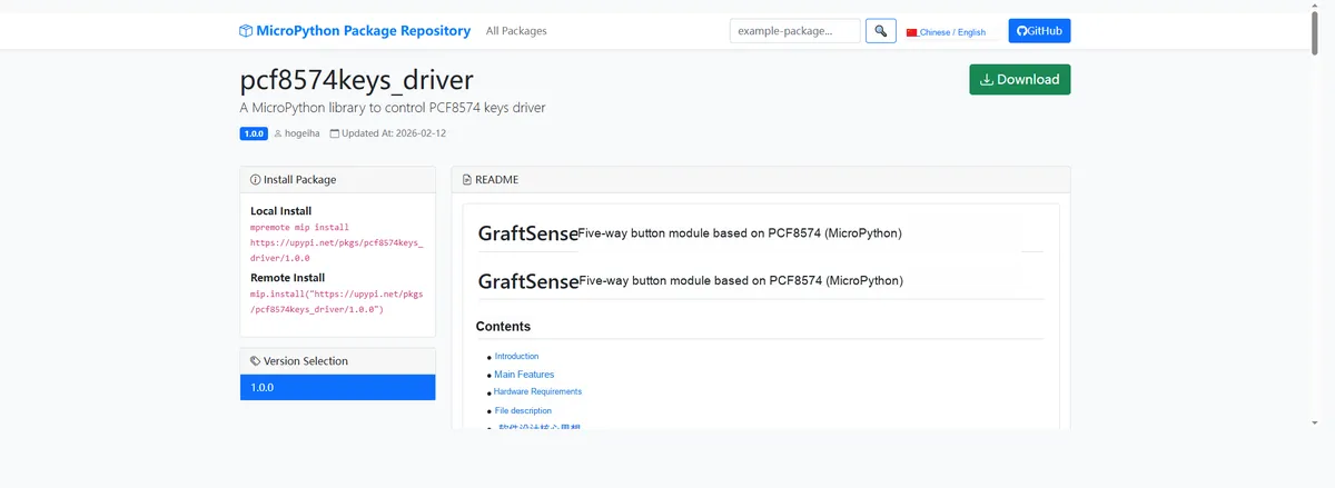
Here, we can use the mip tool to import module driver library code. The following are the usage commands for the mpremote tool:
mpremote mip install github:FreakStudioCN/GraftSense-Drivers-MicroPython/input/pcf8574keys_driverAfter importing the PCF8574 5-way button module - MicroPython driver code, copy the following main.py code into our project:
# Python env   : MicroPython v1.23.0
# -*- coding: utf-8 -*-
# @Time    : 2025/9/8 AM 11:42
# @Author  : 缪贵成
# @File    : main.py
# @Description : Five-way button test file

# ======================================== Import Modules =========================================

from machine import I2C, Pin
import time
from pcf8574 import PCF8574
from pcf8574keys import PCF8574Keys, KEYS_MAP

# ======================================== Global Variables ============================================

# I2C configuration
I2C_ID = 0
# Modify according to actual hardware
SCL_PIN = 5
# Modify according to actual hardware
SDA_PIN = 4

PCF8574_ADDR = None

# ======================================== Functions ============================================

# ======================================== Custom Classes ============================================

# ======================================== Initialization ==========================================

time.sleep(3)
print("FreakStudio:PCF8574 Five-way Button Test Program")
# Initialize I2C
i2c = I2C(I2C_ID, scl=Pin(SCL_PIN), sda=Pin(SDA_PIN), freq=400000)

# Start scanning for devices on the I2C bus and return a list of slave addresses
devices_list: list[int] = i2c.scan()
print('START I2C SCANNER')

# If the devices list is empty, no device is connected to the I2C bus
if len(devices_list) == 0:
    # If not empty, print the slave device addresses
    print("No i2c device !")
else:
    # Iterate over the slave device address list
    print('i2c devices found:', len(devices_list))
for device in devices_list:
    # Check whether the device address is the PCF8574 address
    if 0x20 <= device <= 0x28:
        # Assume the first device found is the PCF8574 address
        print("I2c hexadecimal address:", hex(device))

        PCF8574_ADDR = device
# Initialize PCF8574
pcf = PCF8574(i2c, PCF8574_ADDR)
# Initialize the five-way button
keys = PCF8574Keys(pcf, KEYS_MAP)

# ========================================  Main Program  ============================================

while True:
    # Print the current state of all buttons
    all_states = keys.read_all()
    print(all_states)
    # Check the SW1 and SW2 button states to control the LED on/off
    if keys.read_key('SW1') == True:
        keys.led_on()
    if keys.read_key('SW2') == True:
        keys.led_off()
    # Refresh the status display every 100ms
    time.sleep(0.1)
To flash the code, open a terminal and use the mpremote tool to connect to the main controller; the output is as follows:
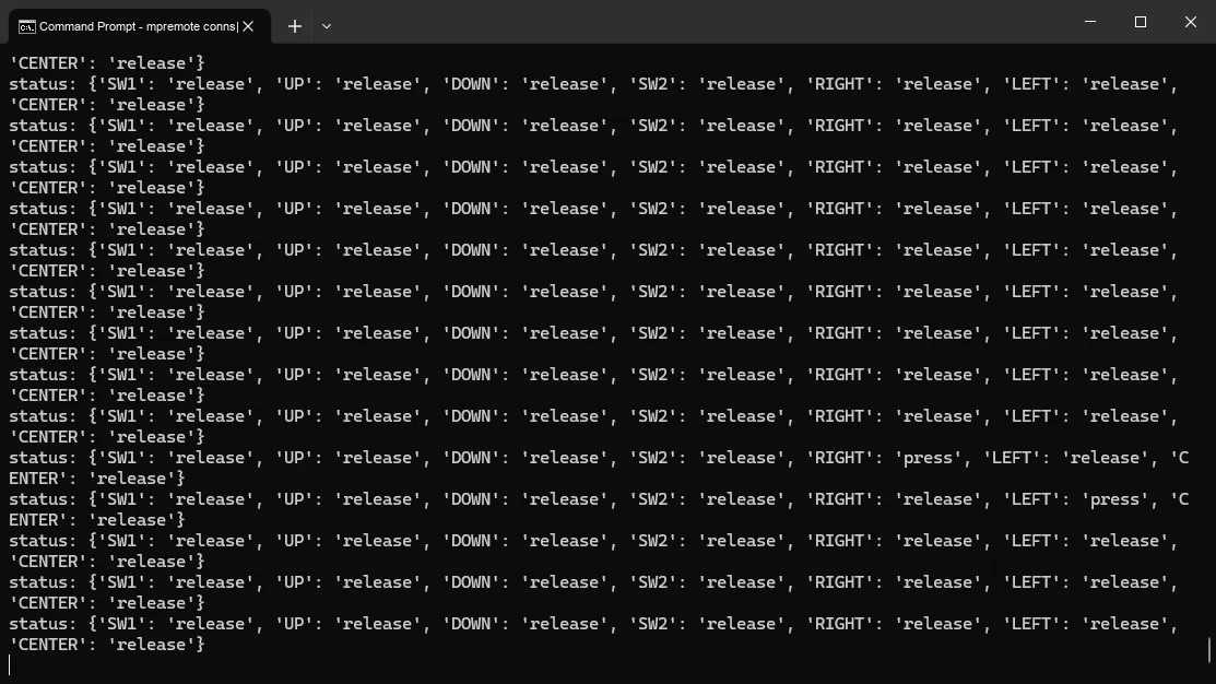
As you can see, when a key is pressed, the corresponding output in the terminal will become press.
IV. Drivers
pcf8574keys_driver.zip 13 KB
5. BOM & Recommended Alternative Parts
None.
VI. Revision History
Document Version | Date of Modification | Modifier | Modified Content |
v1.0 | 2025-11-13 | Ling Gaoxing | Initialize the document |
v1.1 | 2025-12-29 | Li Zisheng | Added application experiments and production files |
v1.2 | 2025-12-31 | Xin Ruili | Create an open version of the document based on the internal document version v1.1. |
v1.3 | 2026-03-29 | Xin Ruili | Modified the application experiment section. |
VII. Relevant Materials
7.1 Chip Datasheet
PCF8574 Manual.pdf 3.4 MB
7.2 Unique Icons for PCB Silkscreen