Contents
- I. Module Introduction
- II. Introduction to Main Chips
- 2.1 Chip Overview
- 2.2 Pin Definition
- 2.3 Functional Block Diagram
- 2.4 Performance Parameters
- 2.5 Reference Circuit
- 2.6 Chip Configuration
- 2.7 Communication Interfaces and Related Protocols
- 2.8 PCB Routing Precautions
- III. Circuit Engineering
- 3.1 Circuit Source Engineering
- 3.2 Module Usage Instructions
- 3.3 Application Experiment
- IV. Drivers
- 5. BOM & Recommended Alternative Parts
- VI. Revision History
- VII. Relevant Materials
- 7.1 Chip Datasheet
- 7.2 PCB Silkscreen Specific Icons
I. Module Introduction
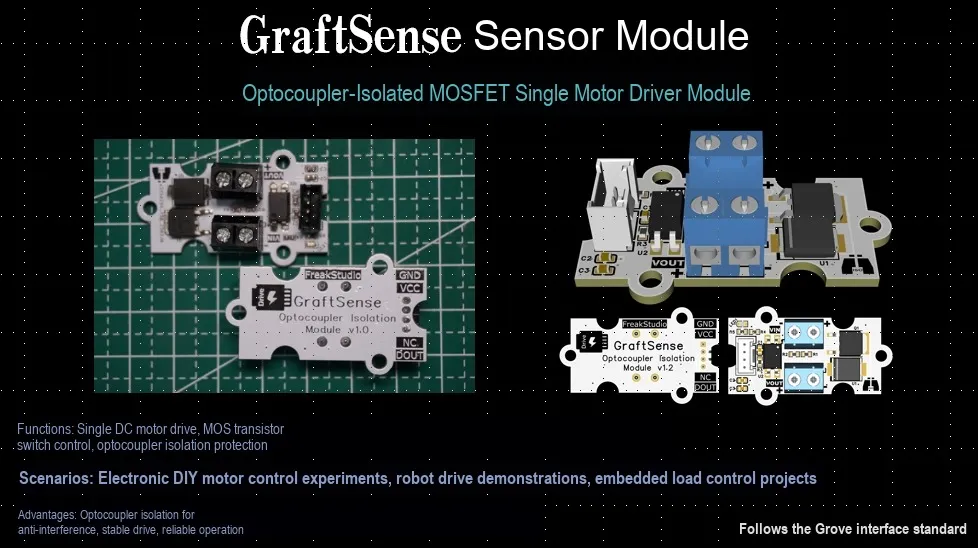
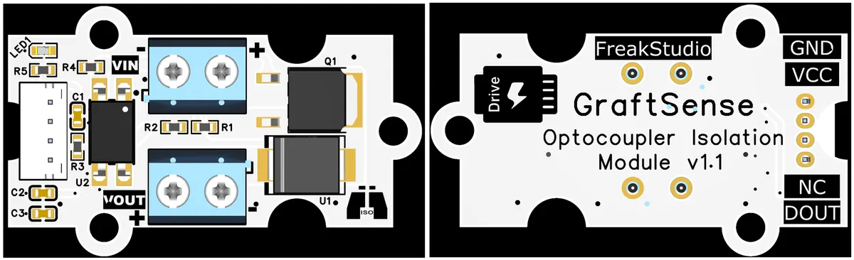
Optocoupler-isolated MOSFET single-motor drive module uses the optocoupler EL817S to realize electrical isolation between the control signal and the power circuit, and drives a single motor with the help of MOS FET IRFR9024N; the module is equipped with VIN power input and VOUT power output interfaces, the CONTROL pin receives the control signal, and after optocoupler isolation, it controls the on-off of the MOS FET to drive the motor;It is also equipped with an indicator light composed of + 5V power supply, a resistor R5 and LED1 to display the working status; the power supply stability is ensured by filter capacitors (such as C2, C3), which not only enhances the anti-interference capability between the control circuit and the motor drive circuit, but also protects the front-end control equipment, making it suitable for safe drive scenarios of a single motor.
For this module, the VIN maximum voltage is recommended to be ≤55V (limited by the withstand voltage of the MOS tube), and the maximum continuous current is recommended to be ≤6.8A (limited by the current-carrying capacity and heat dissipation conditions of the MOS tube).
II. Introduction to Main Chips
The core chip of this module is EL817S optocoupler.
2.1 Chip Overview
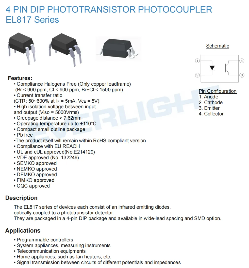
EL817S The optocoupler is a transistor-output photoelectric coupler in 4-pin DIP/SMD packages, composed of an infrared light-emitting diode and a photosensitive transistor optocoupler. It features an input-output isolation voltage of up to 5000Vrms, a creepage distance >7.62mm, a current transfer ratio (CTR) ranging from 50% to 600%(at IF= 5mA, VCE= 5V), an operating temperature range of -55°C to + 110°C, and complies with RoHS as well as certifications including UL and VDE.It can realize isolated signal transmission between circuits with different potentials/impedances, and is suitable for scenarios such as programmable controllers, measuring instruments, and household appliances.
2.2 Pin Definition
| Pin number | Name | Direction | Function description |
|---|---|---|---|
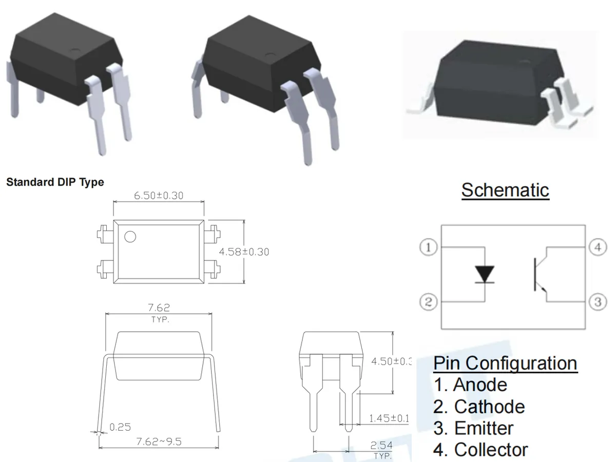
| 1 | A | Input | Optocoupler LED anode, connected to the control signal through current-limiting resistor R3. |
| 2 | C | Input | Optocoupler LED cathode, connected to PGND. |
| 3 | E | Output | Phototransistor emitter, connected to system GND. |
| 4 | C | Output | Phototransistor collector, connected to the MOSFET gate voltage divider network. |
2.3 Functional Block Diagram
EL817S The internal functional block diagram is as follows:
- Input terminal: infrared
LED, which converts current signals into optical signals. - Output Terminal: A phototransistor that turns on upon receiving an optical signal to drive
MOSFETgate potential variation.
2.4 Performance Parameters
2.4.1 Absolute Parameters
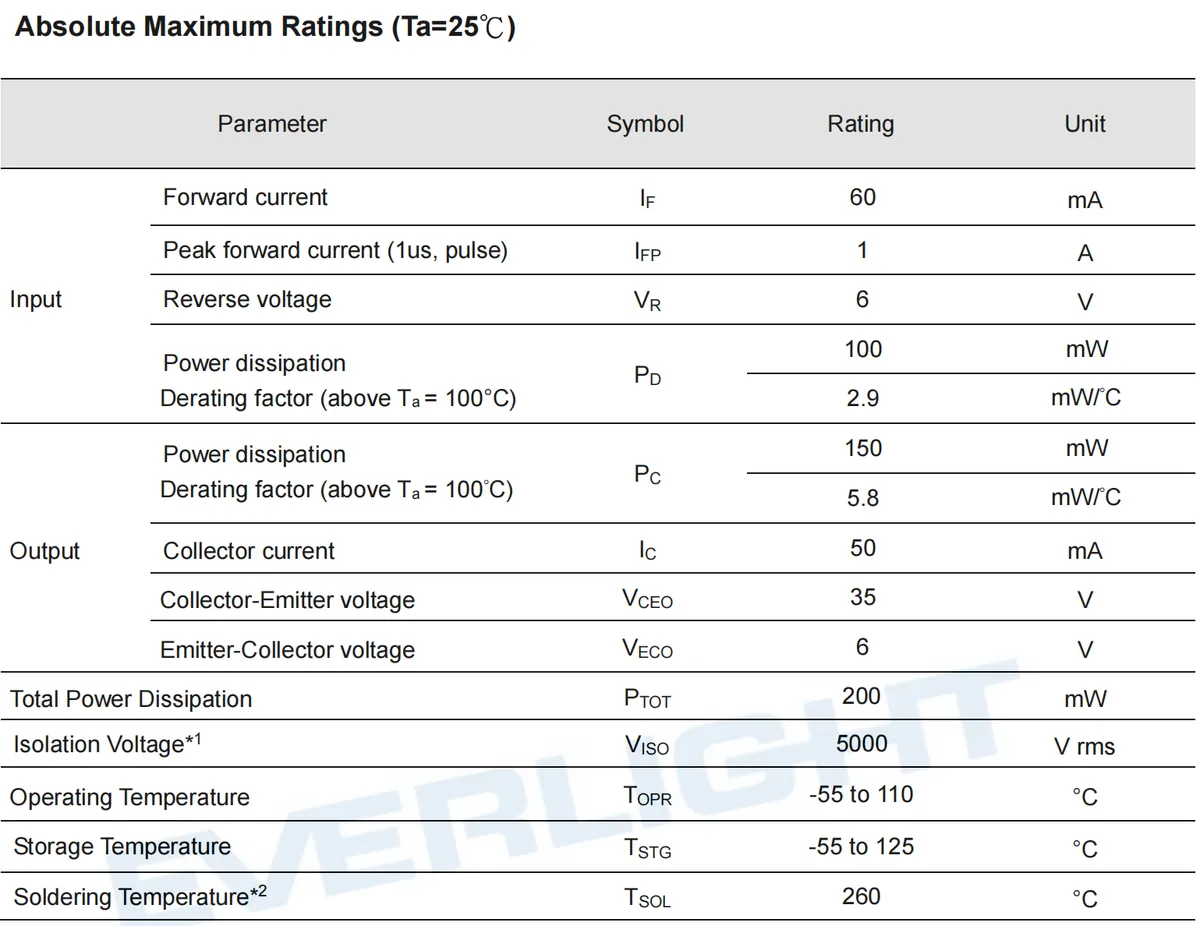
This table presents the absolute maximum ratings for the EL817S optocoupler at an ambient temperature of 25°C, which specify the limiting operating conditions for all dimensions of the device, as interpreted below:
- Input side (light-emitting diode section):
- Forward Current (
I<sub>F</sub>): Maximum 60mA, which is the upper limit of the continuous forward current of the light-emitting diode. - Peak Forward Current (
IFP, 1μs Pulse): 1A, the maximum instantaneous forward current allowed under a short 1-microsecond pulse. - Reverse Voltage (
VR): 6V, which is the upper limit of the reverse voltage that the light-emitting diode can withstand; exceeding this value may easily cause damage to the LED. - Power Consumption (
PD) and Derating: Maximum continuous power consumption: 100 mW; when the temperature exceeds 100°C, the derating factor is 2.9 mW/°C (i. e., for every 1°C increase in temperature, the power consumption must be reduced by 2.9 mW to prevent overheating).
- Forward Current (
- Output side (phototransistor section):
- Power Dissipation (
PC) and Derating: Maximum continuous power dissipation on the collector side is 150mW; when the temperature exceeds 100°C, the derating factor is 5.8mW/°C. - Collector Current (
I_C): 50mA, the maximum current that can be output by the collector of the phototransistor. - Collector-Emitter Voltage (
VCEO): 35V, which is the maximum voltage that can be withstood between the collector and the emitter. - Emitter-collector voltage (
V_ECO): 6 V, the upper limit of reverse withstand voltage between the emitter and the collector.
- Power Dissipation (
- Total Power Consumption and Environmental Parameters:
- Total power consumption (
PTOT): 200mW, which is the upper limit of the total power consumption of the input (light-emitting diode) and the output (phototransistor). - Isolation Voltage (
VISO): 5000V rms, which is the dielectric withstand voltage between the input and output circuits to ensure the safety of electrical isolation. - Operating Temperature (
TOPR):-55~110℃, the temperature range within which the device can operate properly. - Storage Temperature (
TSTG):-55~125℃, the temperature range for device storage. - Soldering Temperature (
TSOL): 260°C, the maximum temperature during soldering operation (needs to be matched with a reasonable soldering duration, usually the upper limit for short-time soldering).
- Total power consumption (
When designing an application, the actual operating parameters must be strictly lower than these rated values; otherwise, device damage or reduced reliability may result.
2.4.2 Photoelectric Characteristic Parameters
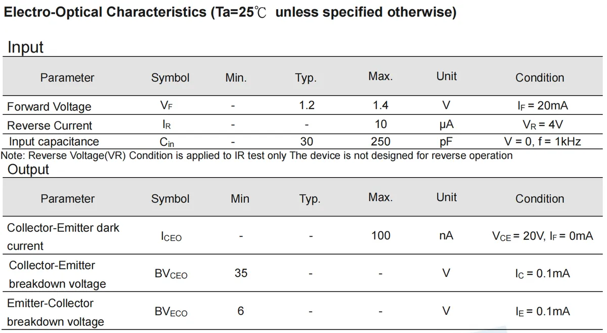
The electro-optical characteristic parameters of EL817S optocoupler at ambient temperature of 25 ℃ are classified and interpreted as follows:
- Input side (light-emitting diode section):
- Forward Voltage (
VF): refers to the voltage drop across both terminals of a light-emitting diode (LED) when it is conducting. The test condition is a forward currentIF= 20mA, with a typical value of 1.2V and a maximum value of 1.4V. When designing the input drive circuit, it is necessary to ensure that the drive voltage can cover this voltage drop to guarantee normal light emission of the diode. - Reverse Current (
IR): the leakage current of a light-emitting diode when subjected to a reverse voltage, with the test condition being a reverse voltageVR= 4Vand a maximum value of 10μA. A smaller value indicates better reverse insulation performance of the diode and lower leakage loss. - Input Capacitance (
Cin): It refers to the capacitance of the input terminal under no bias and at a frequency of 1kHz, with a typical value of 30pF and a maximum value of 250pF. The capacitance value affects high-frequency signal transmission; an excessively large capacitance may cause signal delay or attenuation, which requires special attention when designing high-speed circuits.
- Forward Voltage (
- Output side (phototransistor section):
- Collector-Emitter Dark Current (
ICEO): The leakage current between the collector and emitter when there is no input illumination (IF= 0mA), with the test condition being collector-emitter voltageVCE= 20V, and the maximum value is 100nA. A smaller dark current leads to lower power consumption and better stability of the device in the no-signal state. - Collector-Emitter Breakdown Voltage (
BVCEO): The maximum reverse voltage that can be sustained between the collector and the emitter, measured under the test condition of collector currentIC= 0.1mA, with a minimum value of 35V. In practical applications, the collector-emitter voltage must be strictly lower than this value to prevent breakdown and damage to the device. - Emitter-collector breakdown voltage (
BVECO): This refers to the reverse withstand voltage between the emitter and the collector, measured under the test condition of emitter currentIE= 0.1mA, with a minimum value of 6V. Similarly, the actual voltage must be prevented from exceeding this value to ensure reverse insulation safety.
- Collector-Emitter Dark Current (
These parameters directly determine the device's drive matching, signal transmission efficiency and safe Scope of Work, and serve as the core reference for ensuring performance and reliability in circuit design.
2.4.3 Conversion Characteristics
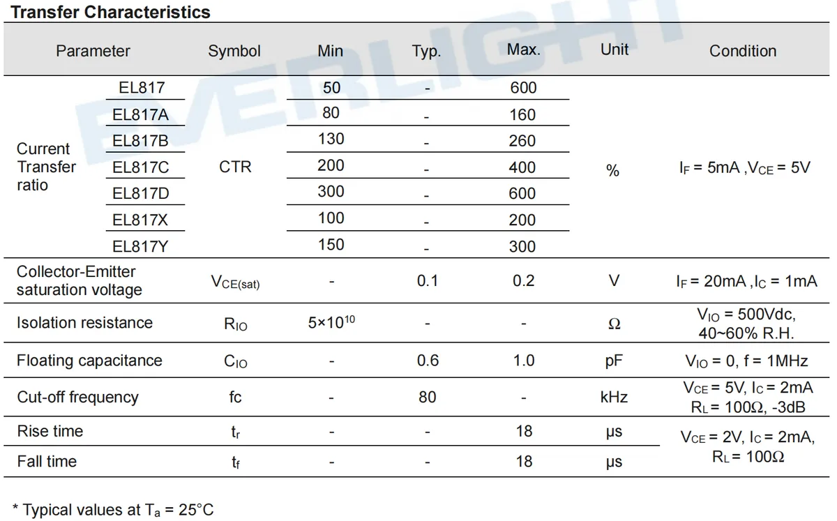
EL817S The transmission characteristic parameters of the optocoupler at an ambient temperature of 25°C can be interpreted from the dimensions of "current transfer, saturation voltage drop, isolation performance, high-frequency characteristics, switching speed", etc. :
- Current Transfer Ratio (
CTR):CTRis the ratio of the collector current of the phototransistor to the forward current of the light-emitting diode (reflecting the photoelectric conversion efficiency). The test conditions areIF= 5mA, VCE= 5V, and theCTRranges vary for different sub-models (EL817/A/B/C/D/X/Y):EL817: Min. 50%, Max. 600%;EL817A: Min. 80%, Max. 160%;EL817B: Min. 130%, Max. 260%;EL817C: Minimum 200%, maximum 400%;EL817D: Minimum 300%, maximum 600%;EL817X: Minimum 100%, maximum 200%;EL817Y: Minimum 150%, maximum 300%.The narrower the CTR (Current Transfer Ratio) range, the better the consistency of devices of the same model; the wider the range, the more flexible the adapted driving/loading scenarios.
- Collector-Emitter Saturation Voltage (
VCE (sat)): refers to the voltage drop between the collector and emitter when the phototransistor is in saturated conduction, with the test conditions beingIF= 20mA, IC= 1mA, a typical value of 0.1V and a maximum value of 0.2V. The smaller this voltage is, the lower the power consumption during saturated conduction and the higher the circuit efficiency will be. - Isolation resistance (
RIO): the insulation resistance between the input and output circuits, measured under the test conditions ofVIO= 500Vdcand ambient humidity of 40~60% RH, with a minimum value of 5×10¹⁰Ω. An extremely high resistance value indicates minimal leakage between the input and output, delivering excellent electrical isolation performance. - Float capacitance (
CIO): The parasitic capacitance between the input and output, measured under the condition ofVIO= 0, f= 1MHz, with a typical value of 0.6pF and a maximum value of 1.0pF. A smaller capacitance leads to lower crosstalk for high-frequency signals, making it more suitable for high-speed isolated transmission scenarios. - Cutoff frequency (
f_c): the -3dB bandwidth of the optocoupler (the frequency at which the signal attenuates by 3dB), measured under the conditions ofVCE= 5V, IC= 2mA, RL= 100Ω, with a typical value of 80kHz. A higher value indicates a stronger response capability of the device to high-frequency signals. - Rise time (
t<sub>r</sub>) and fall time (t<sub>f</sub>):- Rise time: the time required for the output to rise from the low level to the high level, with test conditions being
VCE= 2V, IC= 2mA, RL= 100Ω, maximum value 18μs; - Fall Time: The time required for the output to fall from the high level to the low level, with the same test conditions as above, and the maximum value is 18μs. The shorter the two parameters are, the faster the switching speed of the device will be, making it suitable for high-frequency switching circuits.
- Rise time: the time required for the output to rise from the low level to the high level, with test conditions being
These parameters define the transmission characteristics of optocouplers in terms of aspects such as "energy conversion efficiency", "electrical isolation capability", and "high-frequency/switching performance", serving as the core basis for matching signal rate, power consumption and isolation requirements in circuit design.
2.4.4 Photoelectric Characteristic Curve
These characteristic curves, from the dimensions of temperature, current, and load and other aspects, reveal the performance variation law of the EL817 optocoupler, which has important guiding significance for circuit design:
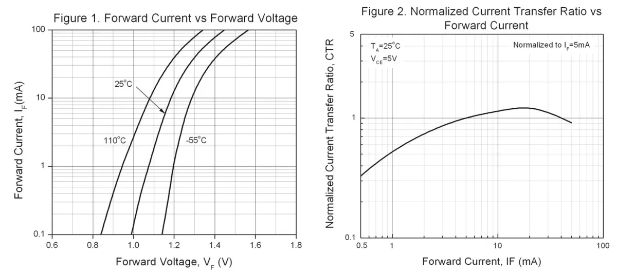
- Figure 1 (Forward Current vs Forward Voltage): The horizontal axis represents the forward voltage of Light Emitting Diode
VF, and the vertical axis represents the forward currentIF, corresponding to the curve. It can be seen that: the lower the temperature, the smaller theIFunder the sameVF(the diode conducts more difficult at low temperatures); the higher the temperature, the larger theIFunder the sameVF(conducts more easily at high temperatures). When designing the driving circuit, the influence of temperature onIFshould be considered to avoid insufficientIFat low temperatures andIFoverload at high temperatures. - Figure 2 (Normalized Current Transfer Ratio vs. Forward Current): The horizontal axis represents
IF, and the vertical axis denotes the normalizedIF= 5mA-referencedCTR(Current Transfer Ratio). The curve first rises and then dips slightly, indicating thatCTRfirst increases with the growth ofIFand then tends to saturate. There exists an "optimalIFrange"(from several mA to a dozen mA) that maximizesCTR(photoelectric conversion efficiency), which should be matched during design to optimize transmission efficiency.
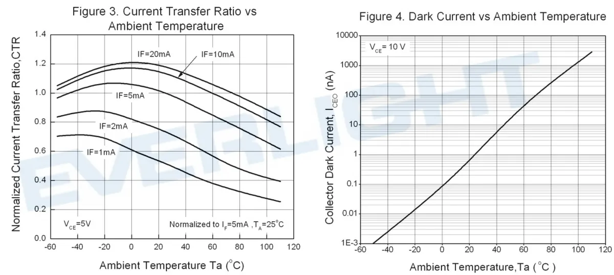
- Figure 3 (Current Transfer Ratio vs. Ambient Temperature): The horizontal axis represents the ambient temperature
Ta, and the vertical axis represents the normalizedCTR(based on the reference value at a specific temperature). The curves correspond to differentIF. It can be seen that: as the temperature rises,CTRdecreases overall; and the smaller theIF, the more significant the impact of temperature onCTR(the curve drops more steeply at lowIF). In high-temperature or low-current scenarios, a margin forCTRattenuation shall be reserved. - Figure 4 (Dark Current vs. Ambient Temperature): The horizontal axis represents
Ta, and the vertical axis represents the collector dark currentICEO(leakage current under no illumination), with the test condition beingVCE= 10V. The curve rises exponentially, indicating that the higher the temperature, the faster the dark current grows — the dark current is extremely low at low temperatures, but can increase to thousands of nA at high temperatures (e. g., 100°C). Excessive dark current will increase static power consumption and the risk of false triggering, so this effect requires attention in high-temperature scenarios.
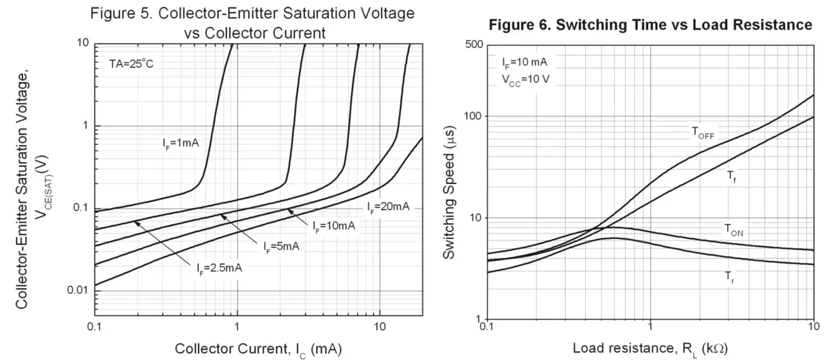
- Figure 5 (Collector-Emitter Saturation Voltage vs. Collector Current): The horizontal axis represents
IC, and the vertical axis representsVCE (sat); the curves correspond to differentIF. It can be seen that:the larger theIF, the smaller theVCE (sat)at the sameIC (the transistor is in deeper saturation with higher efficiency); however, afterICexceeds the threshold,VCE (sat)will rise sharply. During design, it is necessary to balanceIFandICto make the transistor operate in the low saturation voltage drop region. - Figure 6 (Switching Time vs. Load Resistance): The horizontal axis represents the load resistance
RL, the vertical axis represents the switching speed (etc.), along with the test conditions. It can be seen that:the larger theRL, the longer the turn-off time (as the load resistance increases the discharge time constant). For scenarios with high requirements for switching speed, an appropriately smallRLshould be selected to balance speed and power consumption.
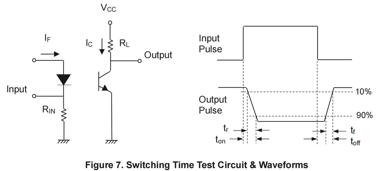
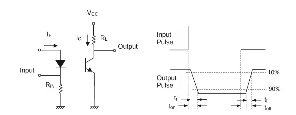
- Figure 7 (Switching Time Test Circuit and Waveforms): The left side shows the test circuit (the input side drives a light-emitting diode, and the output side has a phototransistor connected to a load RL); the right side shows the input/output pulse waveforms, which define rise time
tr(the time for the output to rise from 10% to 90%), fall timetf(the time for the output to fall from 90% to 10%), turn-on timeTON, and turn-off timeTOFF, visually illustrating the physical meaning of "switching speed".
These curves quantify the variations of the "electro-optical conversion - signal transmission - switching characteristics" of the EL817 with external conditions, and serve as the core basis for "matching driving parameters, estimating temperature influence, and optimizing switching speed" in circuit design.
2.5 Reference Circuit
None.
2.6 Chip Configuration
None.
2.7 Communication Interfaces and Related Protocols
None.
2.8 PCB Routing Precautions
None.
III. Circuit Engineering
3.1 Circuit Source Engineering
To obtain the circuit source project, please follow the official account [Freak Embedded]
3.2 Module Usage Instructions
The schematic diagram of this module is shown below:
SCH_Optocoupler-Isolated MOSFET Single Motor Driver Module_v1.1_2025-10-10.pdf 2.1 MB
This module uses digital input DOUT for control: when the input is high, the Light Emitting Diode inside the EL817S optocoupler is turned on to emit light, so that the side of the photosensitive transistor is turned on, and then the gate of the MOS tube IRFR9024NTRPBF provides a driving current, so that the MOS tube is turned on, and a path is formed between VIN and VOUT to power the motor and other loads; when the input is low, the optocoupler stops working, and the MOS tube is turned off because the gate has no driving current, cutting off the power supply circuit from VIN to VOUT .
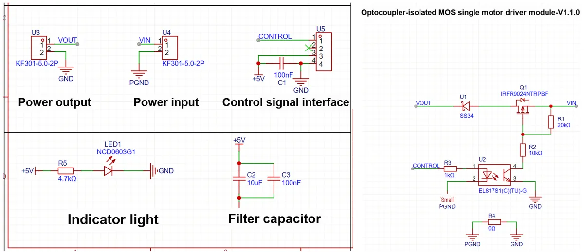
From the perspective of schematic analysis, the circuit can be divided into the core driving and isolation section, the auxiliary function section. In the core section, the optocoupler U2 realizes electrical isolation between the control signal and the power loop, preventing interference from the power side from entering the control side;the MOS transistor Q1, acting as a power switch, is responsible for switching on and off the power supply from VIN to VOUT;the SS34 diode provides freewheeling protection for inductive loads (such as motors), while R1 and R2 respectively provide pull-up and drive current limiting for the gate of the MOS transistor.
In the auxiliary section, the power input interface U4 and output interface U3 complete the connection and output of the power supply; the control signal interface U5 together with the filter capacitor C1 ensures the stable input of the external DOUT control signal; the indicator light LED1 realizes visualization of the working state through current limiting via R5; the filter circuit composed of C2 and C3 filters out the ripple of the + 5V power supply;R4 is a 0Ω resistor used to connect PGND and GND to eliminate ground potential difference interference and unify the ground potential of the circuit.The overall design not only achieves the safety of electrical isolation through optocouplers, but also realizes high-efficiency switching driving for the load by means of MOS tubes.
3.3 Application Experiment
Here, we use the GraftPort-RP2040 development board for testing, and connect the optocoupler-isolated MOSFET single-motor drive module to communicate with the main controller via the DIO interface.
Here, we first use the HY2.0-4P connection cable to connect the module to the GraftPort-RP2040 development board's DIO0 interface:
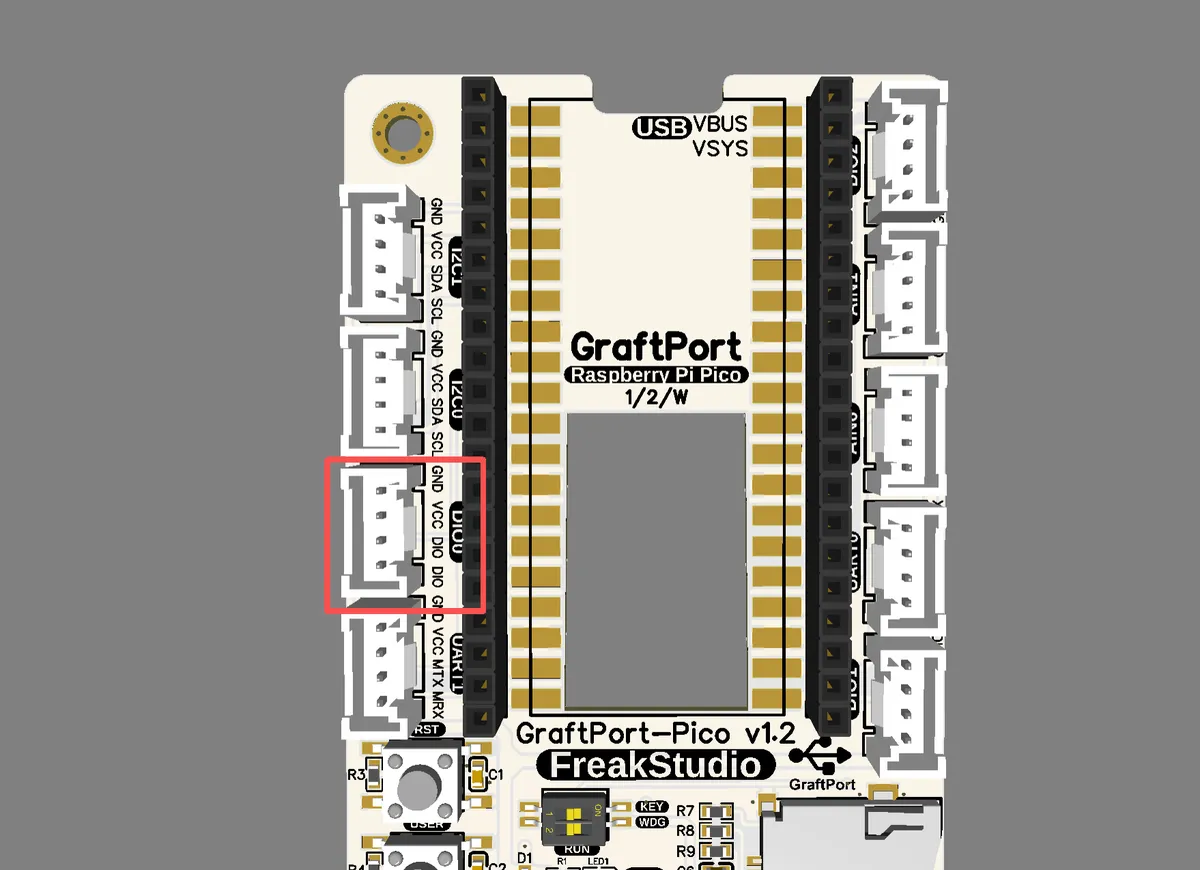
The module connections are shown in the following table:
development board pins | Module Pins | Description |
Pin 6 |
|
|
Pin 7 |
| - |
- |
| Power Supply |
- |
| Power Supply |
- |
| motor |
Here, we need to search for the relevant driver packages on uPyPI: https://upypi.net/zh/

Enter opto_mos_driver to search, and the following will be displayed:

Click to copy the local installation command:

Here, we can import the module driver library code via the mip tool. Below are the usage commands for the mpremote tool:
mpremote mip install github:FreakStudioCN/GraftSense-Drivers-MicroPython/motor_drivers/opto_mos_driverAfter importing the optocoupler-isolated MOSFET single-motor driver module - MicroPython driver code, copy the following main.py code into our project:
# Python env   : MicroPython v1.23.0
# -*- coding: utf-8 -*-
# @Time    : 2025/8/22 9:42 AM
# @Author  : 缪贵成
# @File    : main.py
# @Description : Optocoupler-isolated MOS single motor driver test file

# ======================================== Import Modules =========================================

import time
from machine import Pin, PWM
from opto_mos_simple import OptoMosSimple

# ======================================== Global Variables =============================================

# ======================================== Functions =============================================

# ======================================== Custom Classes =============================================

# ======================================== Initialization configuration ===========================================

#Power-on delay
time.sleep(3)
print("FreakStudio:  OptoMosSimple Test Start ")
# Create a PWM object, output on GPIO6
pwm = PWM(Pin(6))
# Set PWM frequency to 1kHz
pwm.freq(1000)
print("PWM object created on Pin 6 with 1kHz frequency.")

# Create driver instance
driver = OptoMosSimple(pwm)
print("Driver object created.")

# Initialize the driver
driver.init()
print("[init] Initialized ->", driver.get_status())

# ======================================== Main Program ===============================================

# Test the set_duty method
print("[set_duty] Set duty=10000")
driver.set_duty(10000)
print("Status:", driver.get_status())

print("[set_duty] Set duty=70000 (out of range, auto clipped)")
driver.set_duty(70000)
print("Status:", driver.get_status())

# Test the set_percent method
print("[set_percent] Set 25% duty cycle")
driver.set_percent(25.0)
print("Status:", driver.get_status())

print("[set_percent] Set 150% duty cycle (out of range, auto clipped)")
driver.set_percent(150.0)
print("Status:", driver.get_status())

# Test the full_on method
print("[full_on] Full ON")
driver.full_on()
print("Status:", driver.get_status())
time.sleep(5)

# Test the off method
print("[off] Turn OFF")
driver.off()
print("Status:", driver.get_status())
time.sleep(10)

# Test inverted mode (create a new PWM object)
print("[inverted] Testing inverted mode")
pwm_inv = PWM(Pin(16))  # Use a different GPIO to avoid conflict with the driver
pwm_inv.freq(1000)
driver_inv = OptoMosSimple(pwm_inv, inverted=True)
driver_inv.init()
driver_inv.set_percent(30.0)
print("Inverted 30% ->", driver_inv.get_status())
driver_inv.full_on()
print("Inverted full_on ->", driver_inv.get_status())
driver_inv.off()
print("Inverted off ->", driver_inv.get_status())

# Release the resource
print("[deinit] Release resources")
driver.deinit()
driver_inv.deinit()
print("PWM released.")

print("=== OptoMosSimple Test End ===")
To flash the code, open a terminal and use the mpremote tool to connect to the main controller; the output is as follows:
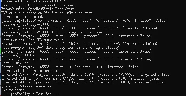
The microcontroller sends a control signal to the module, which triggers after optocoupler isolation MOS tube to turn on; after the motor is powered on and runs for 5 seconds, MOS tube turns off, and the motor stops immediately.
IV. Drivers
opto_mos_driver.zip 9 KB
5. BOM & Recommended Alternative Parts
None.
VI. Revision History
Document Version | Revision Date | Modifier | Revised Content |
v1.0 | 2025-08-31 | Xing Gao | Initialize Document |
v1.1 | 2025-09-21 | Li Zisheng | Added 2.8 PCB routing precautions Revised Section 3, Instructions for Circuit Source Project and Module Usage, and added a secondary heading: 3.1 Circuit Source Engineering, 3.2 Module Usage Instructions, 3.3 Application Experiments The BOM sheet has not been finally checked, the driver has not been re-verified, and the 3.3 application experiment Not yet specified. |
v1.2 | 2025-12-29 | Li Zisheng | Added application experiments and production files |
v1.3 | 2025-12-31 | Sin Ruili | Create an open version of the document based on the internal document version v1.2. |
v1.4 | 2026-03-29 | Sin Ruili | Modified the application experiment section |
VII. Relevant Materials
7.1 Chip Datasheet
EL817S1(C)(TU)-G Datasheet.pdf 1.1 MB
7.2 PCB Silkscreen Specific Icons