Contents
- I. Module Introduction
- II. Introduction to Main Chips
- 2.1 Chip Overview
- 2.2 Pin Definition
- 2.3 Functional Block Diagram
- 2.4 Performance Parameters
- 2.5 Reference Circuit
- 2.6 Chip Configuration
- 2.7 Communication Interfaces and Related Protocols
- 2.8 PCB Routing Precautions
- III. Instructions for Circuit Engineering and Module Usage
- 3.1 Circuit Source Engineering
- 3.2 Module Usage Instructions
- 3.3 Application Experiment
- IV. Drivers
- 5. BOM & Recommended Alternative Parts
- VI. Revision History
- VII. Relevant Materials
- 7.1 Chip Datasheet
- 7.2 Unique Icons for PCB Silk Screen
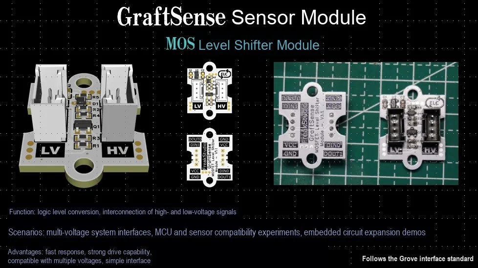
I. Module Introduction
The MOS transistor level conversion module is designed based on 2N7002 MOS transistor and 1N5819WS diode, integrating DC-DC 5V to 3.3V circuit, realizing one-way conversion between 3.3V and 5V levels; it can protect low-voltage chips from high-voltage signal damage, ensure that the high-voltage end reliably recognizes the logic high level, and is suitable for GPIO communication scenarios of different voltage MCUs or devices, providing a secure adaptation scheme for bidirectional signal transmission between 3.3V and 5V systems.
II. Introduction to Main Chips
This module is designed based on 2N7002 MOS transistors and 1N5819WS diodes; since the selected chips are relatively basic, no additional introduction will be provided.
2.1 Chip Overview
None.
2.2 Pin Definition
None.
2.3 Functional Block Diagram
None.
2.4 Performance Parameters
None.
2.5 Reference Circuit
None.
2.6 Chip Configuration
None.
2.7 Communication Interfaces and Related Protocols
None.
2.8 PCB Routing Precautions
None.
III. Instructions for Circuit Engineering and Module Usage
3.1 Circuit Source Engineering
To obtain the circuit source project, please follow the official account [Freak Embedded]
3.2 Module Usage Instructions
The schematic diagram of this module is shown below:
SCH_MOSFET Level Shifter Module_v1.0_2025-11-23.pdf 1.8 MB
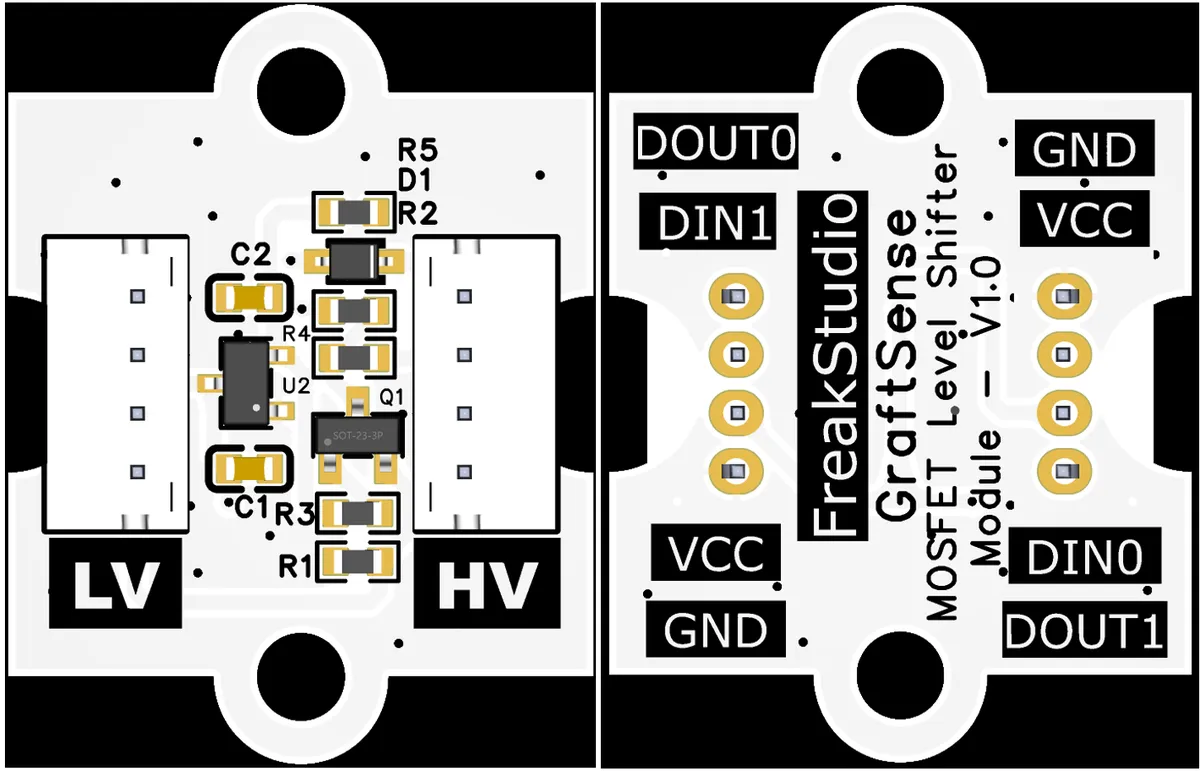
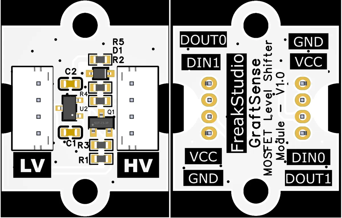
This module is used for the level conversion between the low-voltage side VL (MCU) and the high-voltage side VH (sensor module):
VLterminal'sDOUT1(master control output) corresponds toVHterminal'sDIN1(sensor input);VLterminal'sDIN0(master control input) corresponds toVHterminal'sDOUT0(sensor output).
This module is a unidirectional level conversion circuit, suitable for two MCUs that operate at different voltages to perform GPIO communication (for example, for communication between different units operating at 3.3V and 5.0V respectively: a continuous 5V high-level signal will exceed the withstand limit of a 3.3V chip, thus causing pin damage). However, due to differences in I2C communication conditions, this circuit is not applicable for I2C communication.
When in use, it is necessary to ensure that the high-voltage chip correctly identifies the logic high level:
- Minimum high-level threshold for 5V chips (
VIH): Many 5VMCUsrequire the input logic high-level voltage (VIH) to be at least 3.5V to 4V to be reliably recognized as a logic '1'. - A level shifter can safely boost a 3.3V signal to 5V, ensuring that a 5V
MCUcan reliably recognize a logic '1'.
3.3 Application Experiment
Here, we use the GraftPort-RP2040 development board for testing, and connect the MOSFET level conversion module to the main controller via the DIO interface.
Here, we first use the HY2.0-4P connection cable to connect the module to the GraftPort-RP2040 development board's DIO1 interface:
The core function of this module is to realize bidirectional signal level conversion between different voltage domains (5V and 3.3V voltage standard mutual conversion), and no code is required:
- Low-voltage side (VL) signal transmission:
VLsideDIN1→ after module conversion →VHsideDOUT1(sent to the high-voltage side for reception); Is that correct? - High-voltage side (VH) signal transmission:
VHside DIN0 → after module conversion → VL sideDOUT0(for reception by the low-voltage side).
IV. Drivers
None.
5. BOM & Recommended Alternative Parts
None.
VI. Revision History
Document Version | Revision Date | Modifier | Revised Content |
v1.0 | 2025-11-23 | Li Zisheng | Initialize Document The BOM sheet has not been finally checked, the driver has not been re-verified, and the 3.3 application experiment Not yet specified. |
v1.1 | 2025-12-29 | Li Zisheng | Added application experiments and production files |
v1.2 | 2025-12-31 | Sin Ruili | Create an open version of the document based on the internal document version v1.1. |
VII. Relevant Materials
7.1 Chip Datasheet
C7420321_MOSFET_2N7002_Datasheet_2N7002_REV2.0.PDF 287 KB
C191023_Schottky Diode_1N5819WS_Datasheet_WJ157486.PDF 1.1 MB
7.2 Unique Icons for PCB Silk Screen