Contents
- I. Module Introduction
- II. Introduction to Major Chips
- 2.1 Chip Overview
- 2.2 Pin Definition
- 2.3 Functional Block Diagram
- 2.4 Performance Parameters
- 2.5 Reference Circuit
- 2.6 Chip Configuration
- 2.7 Communication Interfaces and Related Protocols
- 2.8 PCB Routing Precautions
- III. Circuit Engineering
- 3.1 Circuit Source Engineering
- 3.2 Module Usage Instructions
- 3.3 Application Experiment
- IV. Drivers
- 5. BOM & Recommended Alternative Parts
- VI. Revision History
- VII. Relevant Materials
- 7.1 Chip Datasheet
- 7.2 Unique Icons for PCB Silkscreen
I. Module Introduction
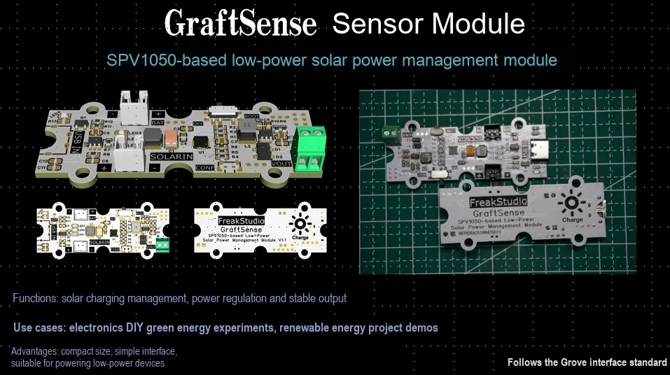
Low-power solar power management module based on SPV1050, compatible with 3.7V single-cell lithium batteries, featuring photovoltaic and USB dual charging functions (solar input voltage range: 0.5V - 4V, continuous charging current: 70mA;USB maximum charging current: 500mA).The module integrates battery protection (overcharge at 4.2V, overdischarge at 3.1V, reverse connection prevention), a 3.3V to 5V DC-DC circuit, a lithium battery reverse connection prevention circuit, etc. It supports stabilizing the maximum power point of solar cells via MPP technology. When the circuit is connected to a battery for the first time with no solar input, the FSW2 tact switch needs to be pressed to activate the circuit. It can supply stable power for low-power devices, and is applicable to scenarios such as solar-powered IoT devices and portable electronic devices, realizing efficient energy management of solar energy and lithium batteries.
II. Introduction to Major Chips
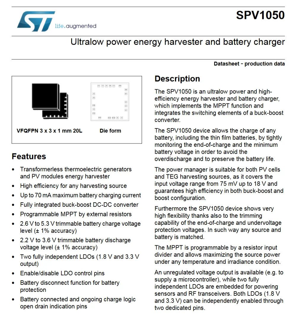
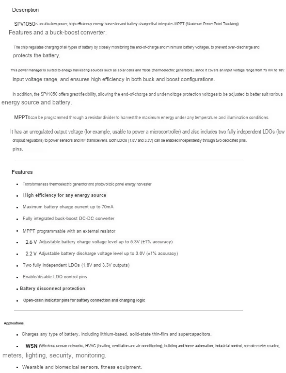
This module adopts the SPV1050 chip for design.
2.1 Chip Overview
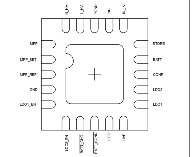
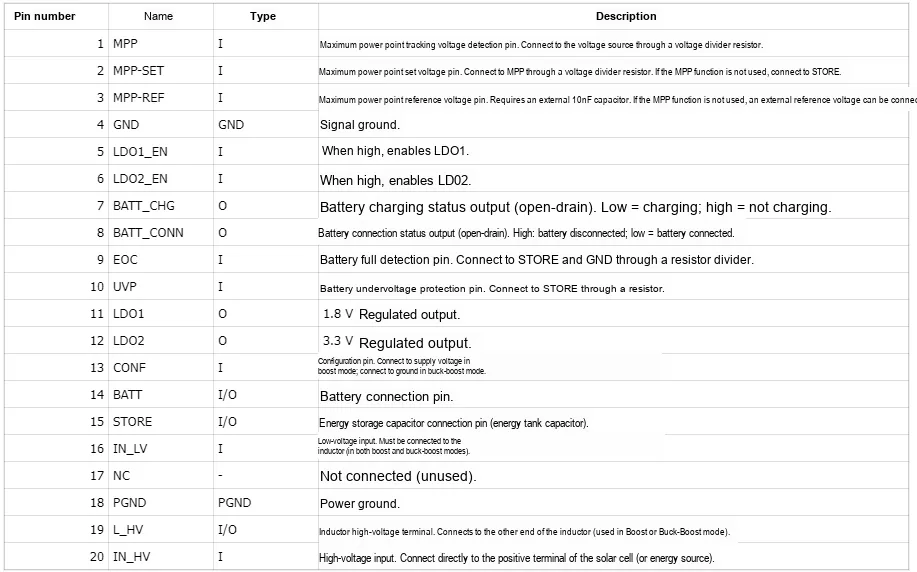
2.2 Pin Definition
2.3 Functional Block Diagram
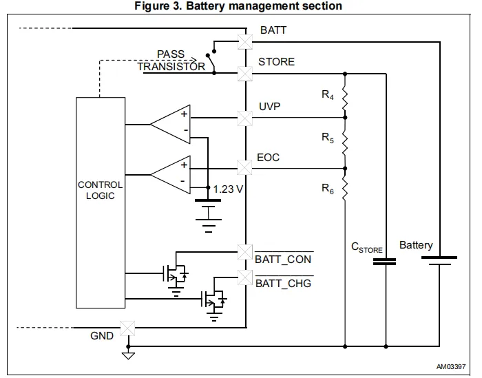
- Control Logic Module (
CONTROL LOGIC): serving as the "core brain" of battery management, it is responsible for integrating signals from various components, outputting control commands, and coordinating the operation of the entire battery management process. - Comparator Module:
- Upper comparator (
+input): Used to monitor the battery voltage (e. g., the terminal voltage atUVP), and participate in logical judgments such as undervoltage protection. - Lower comparator (
-input, reference 1.23V): used to monitor the voltage at theEOCterminal and determine states such as whether charging is complete.
- Upper comparator (
- Switch and Driver Module:
PASS TRANSISTOR: Driven by control logic, it is used to switch the path status of the battery to realize mode switching such as battery storage and power supply.- Two
MOStransistors: controlled by the control logic, used to manage the paths related toBATT_CONandBATT_CHG, so as to realize the battery connection control and charging control.
- Voltage Monitoring and Voltage Divider Module (
R4,R5,R6): Performs voltage division processing on the battery voltage, and transmits the divided voltages to monitoring points such asUVPandEOCrespectively to provide monitoring signals for the comparator. - Energy Storage and Battery Interface Module:
C_STORE: Energy storage capacitor, used for voltage stabilization or temporary energy storage.Battery: The battery body, which serves as the energy object of the entire management system, is connected to the system via interfaces such as BATT.
Typical Scenarios for Battery Charging and Management:
- Charging Monitoring: After the battery voltage is divided by
R4,R5andR6, the voltage at the EOC terminal is input to the lower comparator and compared with the 1.23V reference → the control logic determines whether charging is completed according to the comparison result, and then controls theMOStube in the charging path. - Undervoltage Protection:
UVPterminal voltage is input to the upper comparator → the control logic determines whether an undervoltage condition exists based on the comparison result; if undervoltage is detected, it cuts off the relevant circuit by controlling thePASSTRANSISTORorMOStube to protect the battery.
2.4 Performance Parameters
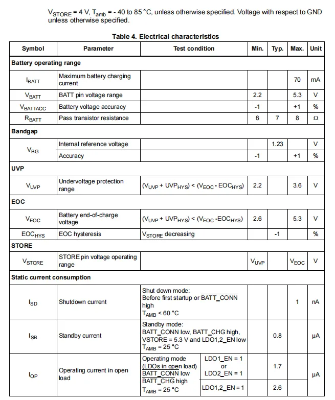
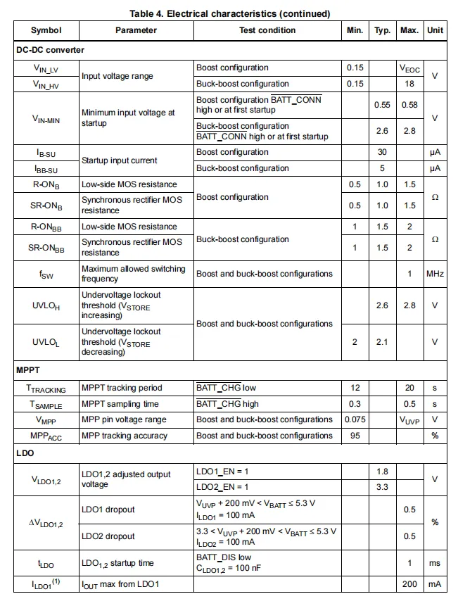
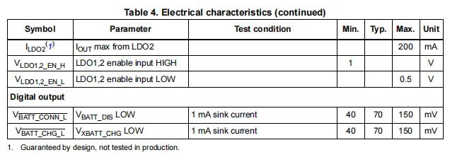
- Battery Scope of Work: Maximum charging current 70mA;
BATTpin voltage range 2.2~5.3V; Battery voltage accuracy -1~+ 1%; Transmission transistor resistance 6~8Ω. - Reference Voltage: Internal reference voltage 1.23V, accuracy: -1% to + 1%.
UVP: Undervoltage protection range: 2.2~3.6V.EOC: End-of-charge voltage: 2.6~5.3V; EOC hysteresis: -1%.STORE: Pin Voltage Scope of WorkV_UVP~V_EOC.- Static Current Consumption: Shutdown current: max. 1 nA; standby current: typical 0.8 μA; no-load operating current: typical 1.7~2.6 μA.
DC-DCconverter:- Input voltage range (boost): 0.15~
V_EOC,(buck-boost): 0.15~18V; - Minimum input voltage for startup: 0.55~0.58V (boost mode), 2.6~2.8V (buck-boost mode);
- Startup input current: 30μA (boost mode), 5μA (buck-boost mode);
- Low-side
MOSresistance (boost): 0.5~1.5Ω, (buck-boost): 1~2Ω; - Synchronous rectification
MOSresistance (boost) 0.5~1.5Ω, (buck-boost) 1~2Ω; - Maximum switching frequency: 1MHz Undervoltage lockout threshold: 2.6~2.8V (rising), 2~2.1V (falling).
- Input voltage range (boost): 0.15~
MPPT: tracking cycle 12~20s; sampling time 0.3~0.5s; pin voltage range 0.075~V_UVP; tracking accuracy 95%.LDO:LDO1.2has typical output voltages of 1.8V and 3.3V; typical dropout of 0.5%; maximum start-up time of 1ms;LDO1/2has a maximum output current of 200mA; the enable input has a high level ≥1V and a low level ≤0.5V.- Digital Outputs:
V_BATT_CONN_L,V_BATT_CHG_Lare 40~150mV at a 1mA sink current.
2.5 Reference Circuit
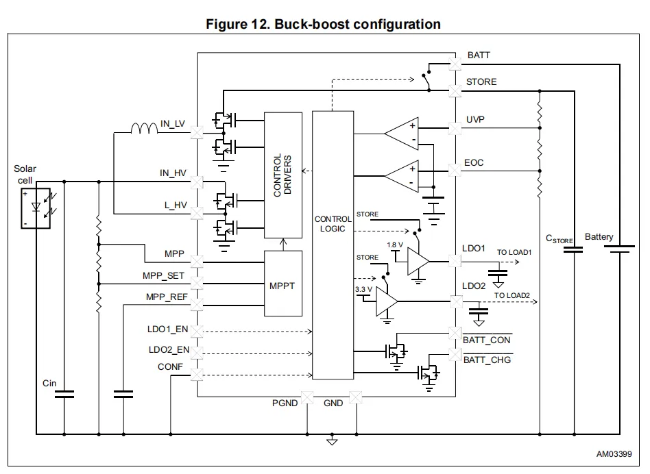
SPV1050 's buck-boost reference circuit, the core function is to collect energy from solar panels: maximize photovoltaic power through built-in MPPT algorithm, and realize safe battery charging through integrated MOSFET 's buck-boost DC-DC conversion (while monitoring the end of charging EOC , under-voltage protection UVP to extend battery life);It can also directly supply power to loads such as LDO through the independently enabled built-in 1.8V/3.3V MCU and sensors, serving as an integrated solution featuring ultra-low-power photovoltaic energy harvesting, battery management and load power supply.
2.6 Chip Configuration
None.
2.7 Communication Interfaces and Related Protocols
This module functions to manage power supply and is not equipped with a communication interface.
2.8 PCB Routing Precautions
None.
III. Circuit Engineering
3.1 Circuit Source Engineering
To obtain the source project of the circuit, please follow the official account [Freak Embedded]
3.2 Module Usage Instructions
SCH_Schematic1_Low-Power Solar Power Management Module Based on SPV1050-V1.1.0_2025-11-10.pdf 2.2 MB
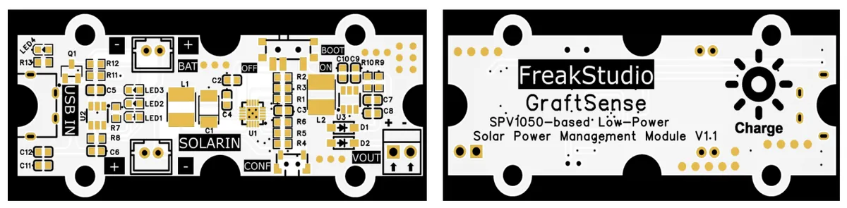
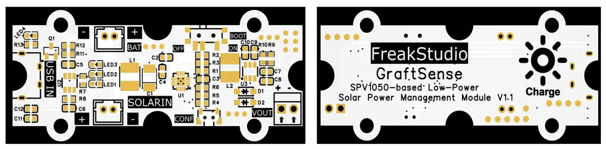
This module provides two charging methods, USB and solar, for single-cell lithium batteries. The descriptions of the interfaces corresponding to each silkscreen marking are as follows:
- “
USB IN” corresponds to the USB port. - “
SOLARIN” corresponds to the solar panel base. - “
BAT” refers to the socket for a single-cell lithium battery. - "
VOUT" corresponds to the output of 5V voltage.
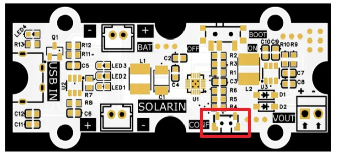
This module will not output + 5V when a battery is connected for the first time and no solar panel is connected. You need to press SW2 tact switch to short the SOLAR_IN pin to the battery voltage to activate the circuit. If a solar panel is connected to the circuit and placed under sunlight, the circuit will automatically activate the output.
3.3 Application Experiment
Here, we use a low-power solar power management module based on SPV1050 connected to a battery for power supply.
(This module supports photovoltaic and USB charging functions, with the input voltage range of the solar panel being 0.5V-4V and the maximum continuous charging current reaching 70mA.
The maximum charging current for USB charging is: 500mA)
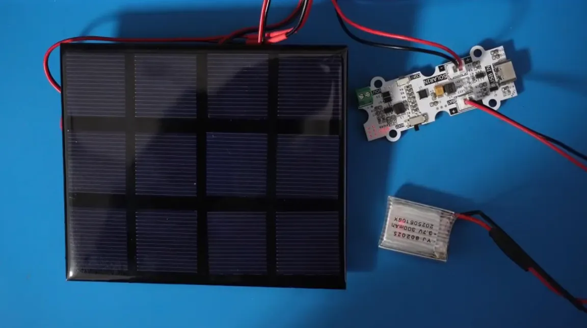
The module connections are shown in the table below:
Solar Panel | Lithium Battery | Module Pins | Description |
- |
|
| - |
- |
|
| - |
- | - |
| Power external output interface |
- | - |
| Power external output interface |
| - |
| Solar Panel |
| - |
| Solar Panel |
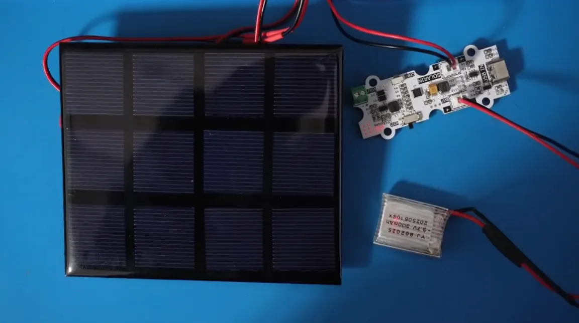
No coding required; it charges the battery when placed in sufficient sunlight.
IV. Drivers
5. BOM & Recommended Alternative Parts
None.
VI. Revision History
Document Version | Date of Modification | Modifier | Modified Content |
v1.0 | 2025-11-10 | Ling Gaoxing | Initialize the document |
v1.1 | 2025-12-29 | Li Zisheng | Added application experiments and production files |
v1.2 | 2025-12-31 | Xin Ruili | Create an open version of the document based on the internal document version v1.1. |
VII. Relevant Materials
7.1 Chip Datasheet
SPV1050 Datasheet.pdf 1.0 MB
ME2159AM6G Datasheet.pdf 300 KB
TP4057 Datasheet.pdf 614 KB
7.2 Unique Icons for PCB Silkscreen