Contents
- I. Module Introduction
- II. Introduction to Major Chips
- 2.1 Chip Overview
- 2.2 Pin Definition
- 2.3 Functional Block Diagram
- 2.4 Performance Parameters
- 2.5 Reference Circuit
- 2.6 Chip Configuration
- 2.7 Communication Interfaces and Related Protocols
- 2.8 PCB Routing Precautions
- III. Circuit Engineering
- 3.1 Circuit Source Engineering
- 3.2 Module Usage Instructions
- 3.3 Application Experiment
- IV. Drivers
- 5. BOM & Recommended Alternative Parts
- VI. Revision History
- VII. Relevant Materials
- 7.1 Chip Datasheet
- 7.2 Unique Icons for PCB Silkscreen
I. Module Introduction
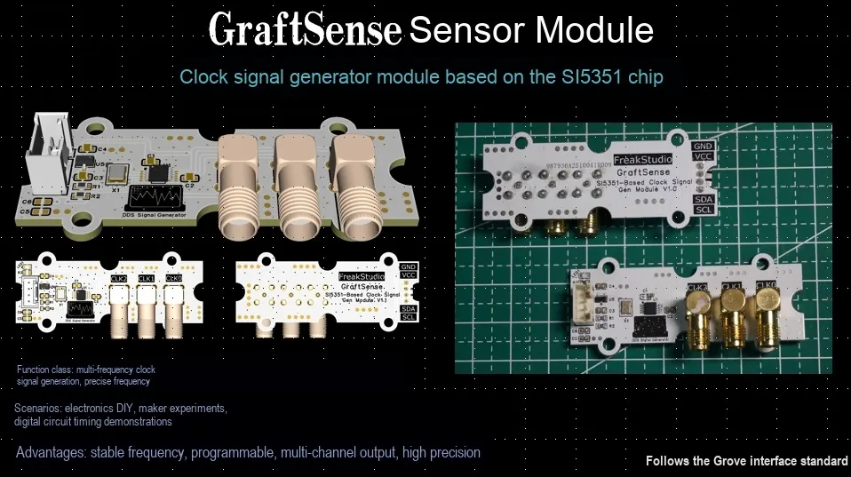
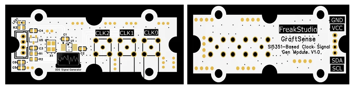
Clock signal generation module based on SI5351 chip, which adopts the SI5351A-B-GTR chip and can generate multiple high-precision clock signals through configuration via the I2C interface. This module is equipped with 3 SMA signal output ports, each supporting a frequency range from 2.5 kHz to 200 MHz, and each output features precise frequency synthesis capability with an error of 0 ppm.It supports fixed-frequency crystals of 25 MHz or 27 MHz, and is suitable for electronic systems such as communication and measurement that require high-precision clock signals, providing a reliable multi-channel clock signal generation solution for them.
II. Introduction to Major Chips
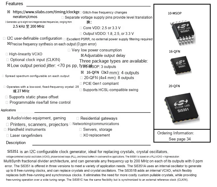
SI5351 is a highly integrated multi-output clock generator chip launched by Silicon Labs, which adopts a PLL and high resolution MultiSynth fractional frequency divider architecture. Its output frequency covers 2.5kHz to 200MHz, with phase noise as low as -155dBc/Hz, low jitter and high frequency accuracy. It has multiple versions of A / B / C, with 3 to 8 output channels, supports various level outputs such as LVDS and CMOS, and can flexibly configure parameters such as output frequency and drive strength through the I2C interface.This chip is compatible with operating voltages of 1.8V/2.5V/3.3V, features an industrial-grade operating temperature range of -40℃ to 85℃, can replace multiple devices such as crystal oscillators and phase-locked loops, is widely used in scenarios including communication equipment, test and measurement instruments, and embedded systems, and delivers the combined advantages of low cost and low power consumption.
2.1 Chip Overview
2.2 Pin Definition
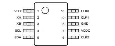
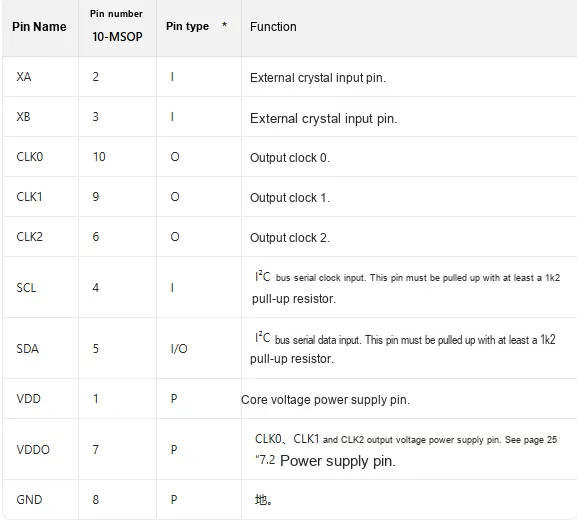
2.3 Functional Block Diagram
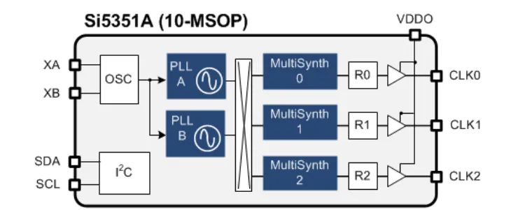
SI5351 The functional block diagram is described as follows:
- Oscillation and Phase-Locked Module
- OSC (Oscillator): Generates an initial clock signal by connecting an external crystal oscillator or clock source through the
XAandXBpins. - PLL A and PLL B (Phase-Locked Loops): Perform phase-locked frequency multiplication on the clock signal output by the oscillator to generate a highly stable intermediate-frequency clock signal.
- OSC (Oscillator): Generates an initial clock signal by connecting an external crystal oscillator or clock source through the
- Frequency Synthesis Module
- MultiSynth 0, MultiSynth 1, MultiSynth 2 (Multi-Synthesizer): perform frequency division, mixing and other processing on the intermediate frequency signal output by the PLL to generate three independent target frequency signals.
- R0, R1, R2 (frequency dividers): further divide the signal output by MultiSynth to finely adjust the output frequency.
Typical Application Scenarios of Multi-Channel Clock Generation:
- Clock Generation: The OSC generates the initial clock → PLL A/B multiplies its frequency → MultiSynth 0/1/2 combines with R0/R1/R2 for frequency division to synthesize the target frequency → CLK0/1/2 outputs three independent clocks.
- Configuration and Control: The external main controller sends configuration commands via the I²C interface → the internal modules of the chip adjust the parameters of the PLL, MultiSynth and frequency dividers according to the commands → so as to realize the precise adjustment of the output clock frequency.
2.4 Performance Parameters
SI5351 Input Clock Characteristics:
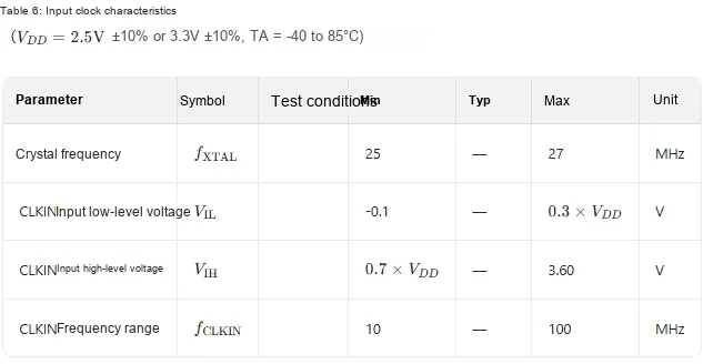
Some parameters in the table are as follows:
- Crystal frequency 25~27MHz;
- CLKIN input low-level voltage ≤ 0.3 × VDD, input high-level voltage ≥ 0.7 × VDD;
- CLKIN Frequency Range: 10~100MHz.
SI5351 Output Clock Characteristics:
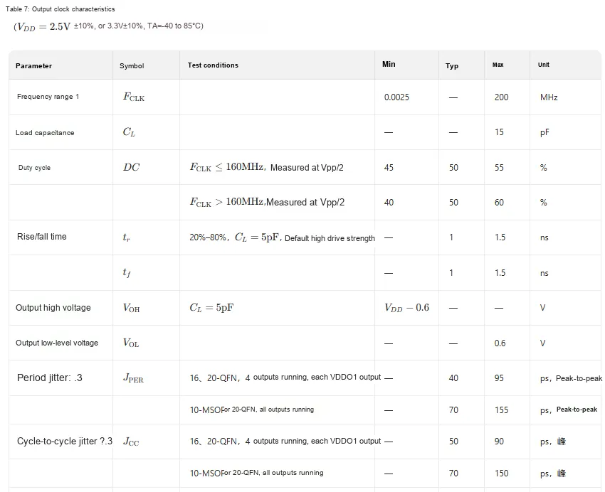
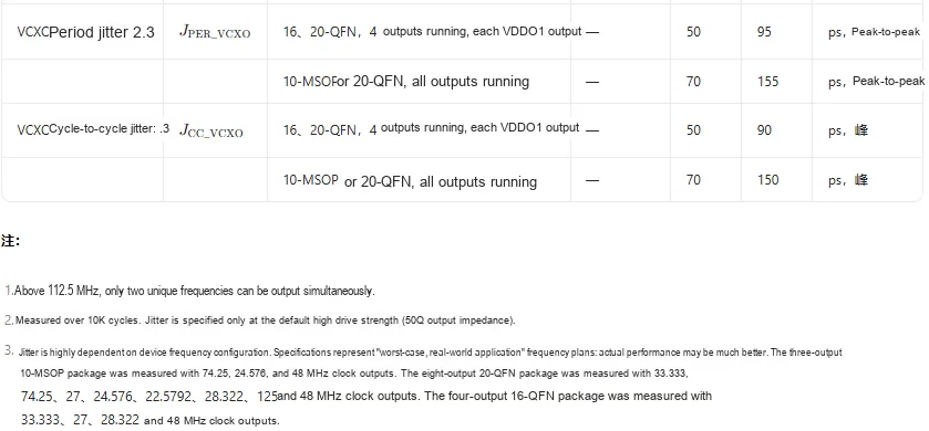
Some parameters in the table are as follows:
- Frequency Range 0.0025~200MHz;
- Load Capacitance Max. 15pF;
- Duty cycle 40%~60%;
- Rise / Fall Time Typical 1ns, Maximum 1.5ns;
- Output high-level voltage ≥ VDD − 0.6V, low-level voltage ≤ 0.6V;
- Cycle-to-cycle jitter Typical: 40~70ps, Maximum: 95~155ps Period jitter Typical: 50~70ps, Maximum: 90~150ps
SI5351 Electrical Parameter Characteristics:
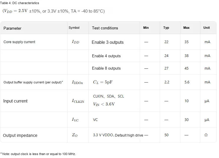
Some parameters in the table are as follows:
- Supply Current: When the core supply current enables 3 outputs, it is typically 22mA with a maximum of 35mA;when 4 outputs are enabled, it is typically 24mA with a maximum of 38mA;when 8 outputs are enabled, it is typically 27mA with a maximum of 45mA;
- Output buffer supply current per channel: typical 2.2mA, maximum 5.6mA (CL = 5pF).
- Input current: The maximum input current of CLKIN, SDA, and SCL is 10μA (when V IN<3.6V), and the maximum input current of VC is 30μA.
- Output Impedance: Typical 50Ω(at 3.3V VDDO, default high-drive setting).
2.5 Reference Circuit
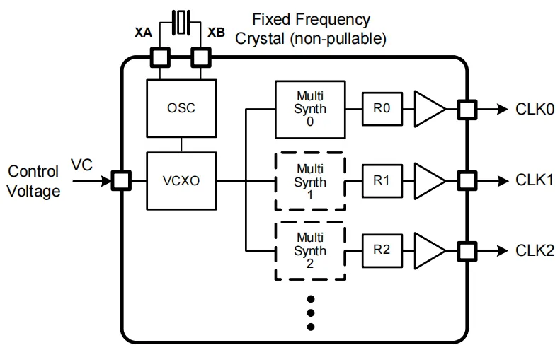
This schematic diagram illustrates the application of the Si5351A clock generator chip: with a fixed-frequency crystal oscillator input, after being processed by the internal oscillator (OSC) and phase-locked loop (PLL), it outputs 3 clock signals of different frequencies via multiple Multi Synths, which can provide clocks for peripheral devices and replace traditional crystal oscillators, oscillators and phase-locked loops.
2.6 Chip Configuration
None.
2.7 Communication Interfaces and Related Protocols
Si5351 has many functions and features that can be controlled by reading from and writing to its RAM space via the I²C interface. Below is a list of common functions controllable through the I²C interface.
- Read status indicator
- Crystal oscillator reference signal lost, LOS_XTAL, reg0 [3]
- CLKIN signal loss, LOS_CLKIN, reg0 [4]
- PLLA and/or PLLB loss of lock, LOL_A or LOL_B, reg0 [6:5]
- Configuration of Multiplication and Division Values for PLL and MultiSynth Frequency Dividers
- Configuration of the spread spectrum profile (downspread or center spread, modulation percentage)
- Cross-point switch selection control for each PLL and MultiSynth frequency divider
- Output Clock Option Settings
- Enable / Disable for each clock output
- Inverted / non-inverted per clock output
- Output frequency division value (2n, n= 1.. 7)
- Output status when disabled (hold high, hold low, high impedance)
- Output phase offset
The I²C interface operates in slave mode, uses 7-bit addressing, can work in standard mode (100 kbps) or fast mode (400 kbps), and supports burst data transmission with automatic address increment.
As shown in Figure 5, the I²C bus consists of a bidirectional serial data line (SDA) and a serial clock input (SCL). According to the recommendations of the I²C specification, both the SDA and SCL pins must be connected to the VDD power supply via external pull-up resistors.
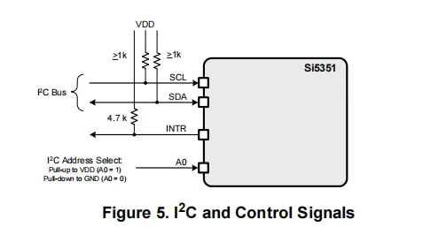
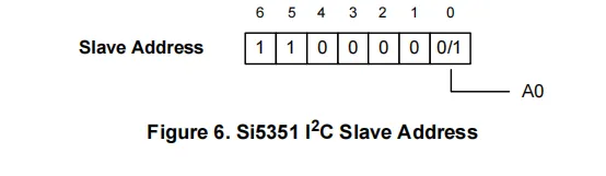
The 7-bit device (slave) address of the Si5351 consists of a 6-bit fixed address and a user-selectable least significant bit (LSB), as shown in Figure 6. The LSB can be selected as 0 or 1 via the optional A0 pin, which is useful for applications that require multiple Si5351 devices on a single I²C bus. Only the Si5351A 20-QFN and Si5351A 16-QFN feature the A0 LSB pin option.If the device does not have an A0 pin, the default address is 0x60 and the A0 bit is set to 0.
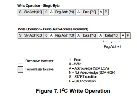
Data transmission follows the provisions of the I²C specification, transmitting the most significant bit (MSB) first in the form of 8-bit words. The write command consists of a 7-bit device (slave) address + write bit, an 8-bit register address, and 8-bit data, as shown in Figure 7. The write burst operation is also illustrated, in which each additional data word is written using an auto-incrementing address.
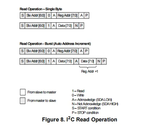
A read operation consists of two phases. First, the register address is set via data writing, and then a data read is performed to retrieve data from the set address. Read burst operations are also supported, as shown in Figure 8.
The timing specifications and Sequence Diagram of the I²C bus are compatible with the I²C bus standard. To ensure compatibility with the SMBus interface, SDA timeout is supported.
2.8 PCB Routing Precautions
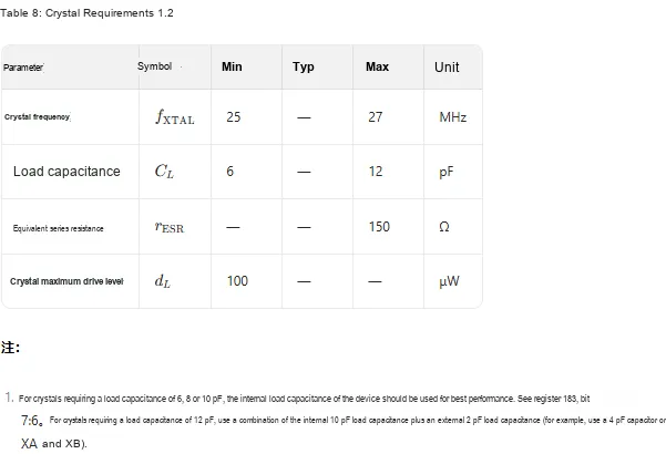
The SI5351 chip has specific requirements for the crystal oscillator used, and the detailed requirements are shown in the table below.
III. Circuit Engineering
3.1 Circuit Source Engineering
To obtain the source project of the circuit, please follow the official account [Freak Embedded]
3.2 Module Usage Instructions
SCH_Schematic1_Clock Signal Generator Module Based on SI5351 Chip-V1.0.0_2025-11-17.pdf 2.2 MB
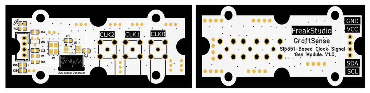
This module adopts IIC communication; when communicating with an external microcontroller, SCL can be directly connected to the SCL pin of the MCU, and SDA can be directly connected to the SDA pin of the MCU.
The interface for clock signal output adopts SMA female connector; a coaxial cable is required for use, and the cable type can be SMA to BNC cable.
3.3 Application Experiment
Here, we use the GraftPort-RP2040 development board for testing, and the clock signal generation module based on the SI5351 chip thereon communicates with the main controller via the I2C interface.
Here, we first use the HY2.0-4P cable to connect the module to the GraftPort-RP2040 development board's I2C0 interface:
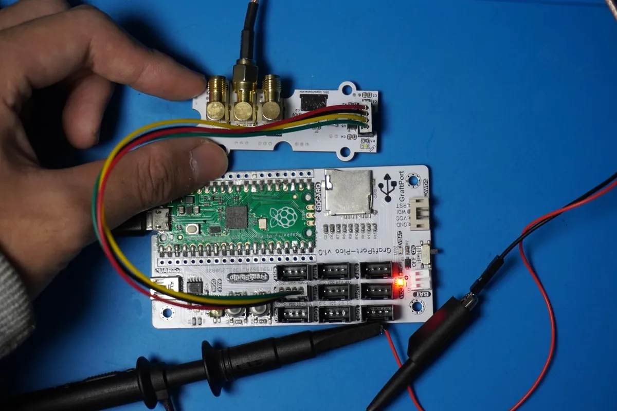
The module connections are shown in the table below:
Development Board Pins | Module Pins | Description |
Pin 4 |
|
|
Pin 5 |
|
|
- |
|
|
- SMA partial wiring: on the module
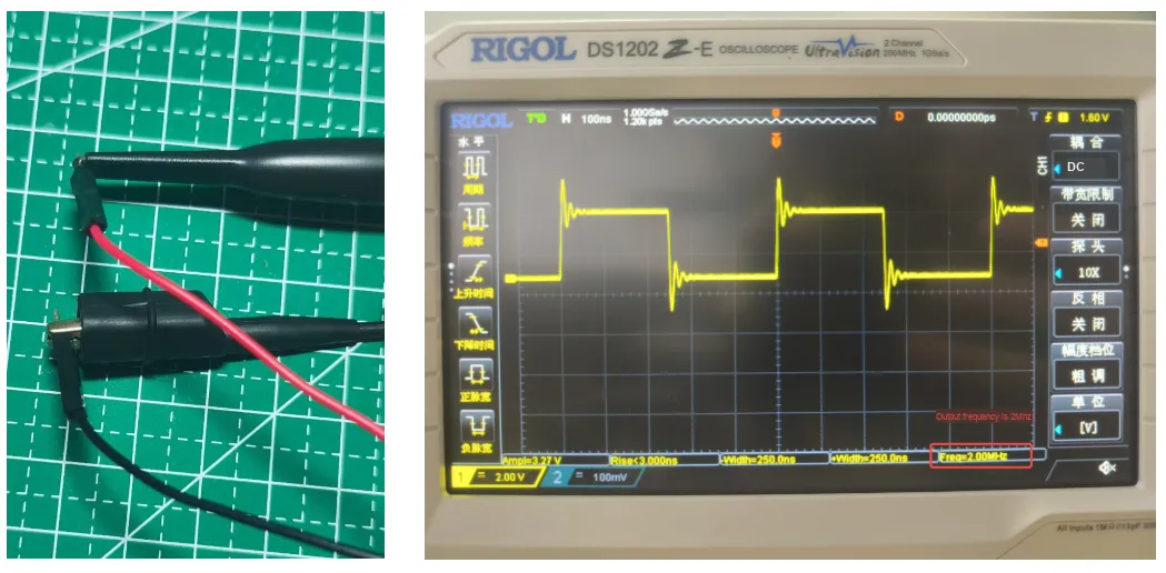
SMAfemale connector (module pin), via theSMAto DuPont cable male end to connect with it (i. e., the male end of the adapter cable is inserted into the module'sSMAfemale connector) to complete the connection on the module side. - Oscilloscope wiring:
SMAto the other end of the DuPont wire (the DuPont wire end)- Red DuPont line : connected to the oscilloscope probe signal terminal female head (usually the metal interface of the probe front end, corresponding to the signal input);
- Black DuPont wire: connects to the ground clip / female ground terminal of the oscilloscope probe (the black ground clip port included with the probe, corresponding to circuit ground).
Here, we need to search for the relevant driver packages on uPyPI: https://upypi.net/zh/
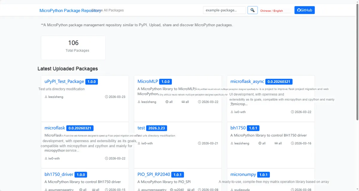
Enter si5351_driver to search, and the following will be displayed:

Click to copy the local installation command:
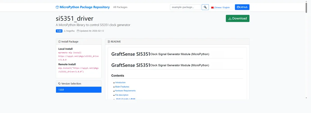
Here, we can use the mip tool to import module driver library code. The following are the usage commands for the mpremote tool:
mpremote mip install github:FreakStudioCN/GraftSense-Drivers-MicroPython/signal_generation/si5351_driverImport the MicroPython driver code for the silicon5351 clock signal generation module, then copy the following main.py code into our project:
# Python env   : MicroPython v1.23.0
# -*- coding: utf-8 -*-
# @Time    : 2025/09/08 10:00
# @Author  : 侯钧瀚
# @File    : mian.py
# @Description : silicon5351 clock example for MicroPython

# ======================================== Import Modules =========================================

# Import MicroPython built-in libraries
from machine import Pin, I2C
# Import the time module
import time
# Import silicon5351
from silicon5351 import SI5351_I2C

# ======================================== Global Variables ============================================

# Crystal frequency 25 MHz
crystal = 25e6
# PLL multiplier (25MHz * 15 = 375 MHz)
mul = 15
# Output frequency 2 MHz (max 200 MHz)
freq = 2.0e6
# Quadrature output flag (minimum output frequency = PLL / 128)
quadrature = True
# Inverted output flag (ignored in quadrature mode)
invert = False

# ======================================== Functions ============================================

# ======================================== Custom Classes ============================================

# ======================================== Initialization ==========================================

# Power-on delay of 3 s
time.sleep(3)
# Print debug message
print("FreakStudio: Use silicon5351 to output clock signals.")
i2c = I2C(0, scl=Pin(5), sda=Pin(4), freq = 100000)

# Initialize SI5351 chip
si = SI5351_I2C(i2c, crystal=crystal)
# Configure PLL0 = 375 MHz
si.setup_pll(pll=0, mul=mul)
# Initialize output channels 0 and 1, using PLL0
si.init_clock(output=0, pll=0)
# Set output frequency to 2 MHz (based on fixed PLL)
si.set_freq_fixedpll(output=0, freq=freq)

# ========================================  Main Program  ===========================================

# Enable outputs 0 and 1
si.enable_output(output=0)
print(f'done freq={freq} mul={mul} quadrature={quadrature} invert={invert}')
# Keep output on for 20 seconds
time.sleep(20)
# Disable output 0
si.disable_output(output=0)
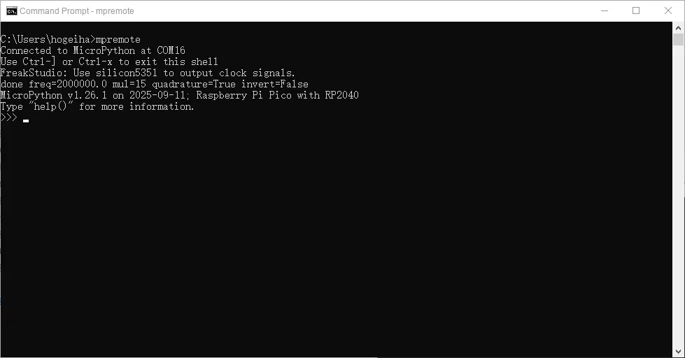
Burn the code, open the terminal, and use the mpremote tool to connect to the main controller. The output is as follows:
After connecting the signal probe of the oscilloscope, click AUTO to perform sampling, and observe the oscilloscope:
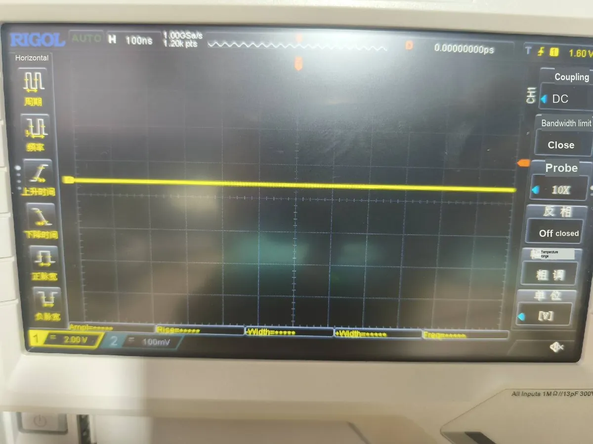
The channel will be turned off after 20 seconds of output, which means the signal stops square wave output:
IV. Drivers
si5351_driver.zip 15 KB
5. BOM & Recommended Alternative Parts
None.
VI. Revision History
Document Version | Date of Modification | Modifier | Modified Content |
v1.0 | 2025-11-17 | Ling Gaoxing | Initialize the document |
v1.1 | 2025-12-10 | Ling Gaoxing | 1. Supplementary description for the reference circuit section in Subsection 2.5; 2. Move the crystal oscillator selection description in Subsection 2.6 to Subsection 2.8; 3. Add the SMA interface part to the module usage instructions in Subsection 3.2 |
v1.2 | 2025-12-29 | Li Zisheng | Added application experiments and production files |
v1.3 | 2025-12-31 | Xin Ruili | Create an open version of the document based on the internal document version v1.2. |
v1.4 | 2026-03-29 | Xin Ruili | Modified the application experiment section |
VII. Relevant Materials
7.1 Chip Datasheet
SI5351A-B-GTR Datasheet.pdf 1.7 MB
Crystal Oscillator Datasheet.pdf 1.1 MB
7.2 Unique Icons for PCB Silkscreen