Contents
- I. Module Introduction
- II. Introduction to Major Chips
- 2.1 Chip Overview
- 2.2 Pin Definition
- 2.3 Functional Block Diagram
- 2.4 Performance Parameters
- 2.5 Reference Circuit
- 2.6 Chip Configuration
- 2.7 Communication Interfaces and Related Protocols
- 2.8 PCB Routing Precautions
- III. Circuit Engineering
- 3.1 Circuit Source Engineering
- 3.2 Module Usage Instructions
- 3.3 Application Experiment
- IV. Drivers
- 5. BOM & Recommended Alternative Parts
- VI. Revision History
- VII. Relevant Materials
- 7.1 Chip Datasheet
- 7.2 Unique Icons for PCB Silkscreen
I. Module Introduction
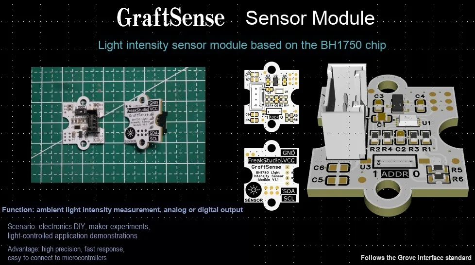
Light intensity sensor module based on BH1750 chip, designed with BH1750FVI-TR ambient light sensor, communicates with microcontrollers via I2C. The sensor integrates a built-in photodiode that converts light illumination into analog current signals, which are then converted into digital values by an analog-to-digital converter (ADC), enabling accurate measurement of ambient light intensity. It features a typical operating current of 16μA in continuous low resolution mode and 120μA in high resolution mode, making it suitable for scenarios requiring light intensity sensing such as smart lighting and environmental monitoring, and providing a reliable light intensity detection solution for devices.
II. Introduction to Major Chips
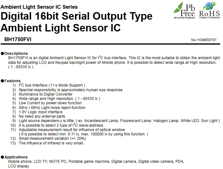
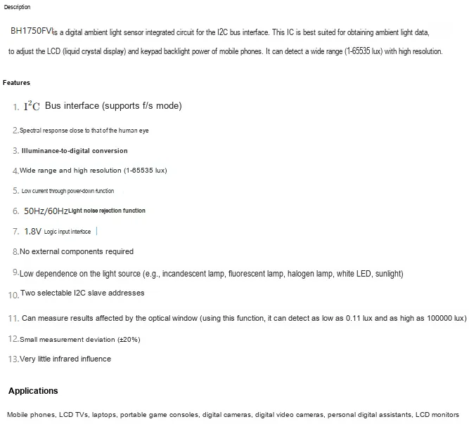
BH1750FVI-TR is a low-power digital ambient light sensor with a built-in high-sensitivity photodiode and signal processing circuit. It can accurately detect visible light in the 400~700nm band, featuring a wide measurement range (1~65535) and high accuracy (typical ±20%), and can output digital illumination intensity data via the I²C interface. It supports a 2.4~3.6V power supply, with extremely low power consumption (approximately 120μA in operating mode and only 1μA in standby mode). Adopting a compact SMD package and compliant with the RoHS standard, it is widely used in scenarios requiring light detection such as smartphones, automatic display brightness adjustment, smart homes, and security equipment.
2.1 Chip Overview
2.2 Pin Definition
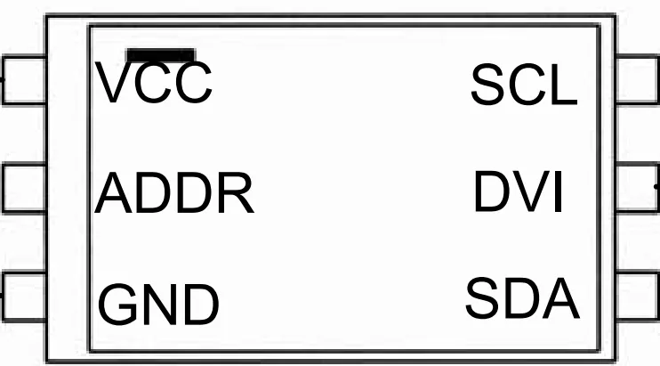
Pin Description
| Pin number | Pin name | Equivalent circuit | Function |
| 1 | VCC | Power supply terminal | |
| 2 | ADDR | I²C slave address terminal. When ADDR = 'H' (ADDR ≥ 0.7Vcc), the address is "1011100"; when ADDR = 'L' (ADDR ≤ 0.3Vcc), the address is "0100011". The ADDR terminal is designed with a tri-state buffer for internal testing, so pay attention to the VCC and DVI power-up sequence. | |
| 3 | GND | Ground terminal | |
| 4 | SDA | I²C bus interface SDA terminal | |
| 5 | DVI | The DVI terminal is an asynchronous reset terminal for the internal registers. Therefore, set it to 'L' (for at least 1μs, DVI ≤ 0.4V) after Vcc is applied. The BH1750FVI is pulled down by a 150kΩ resistor when DVI = 'L'. | |
| 6 | SCL | I²C bus interface SCL terminal |
2.3 Functional Block Diagram
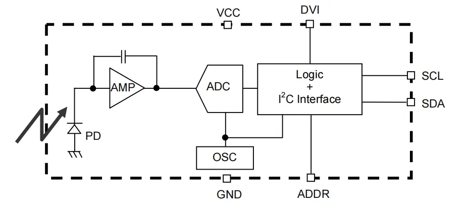
The functional block diagram described above is explained as follows:
PD(photodiode) is a photodiode with a response close to that of the human eye.AMP(amplifier) is an integrating operational amplifierPDused to convert current into voltage.ADC(Analog-to-Digital Converter) is an analog-to-digital converter used to acquire 16-bit digital data.- Logic +
I²Cinterface ambient light calculation andI²Cbus interface. It contains the following registers:- Data register → Used to store ambient light data, with an initial value of "0000_0000_0000_0000".
- Measurement time register → Used to store the measurement time, with an initial value of "0100_0101".
OSC(Oscillator) Internal oscillator (typical value: 320kHz), which provides a clock for the internal logic.
2.4 Performance Parameters
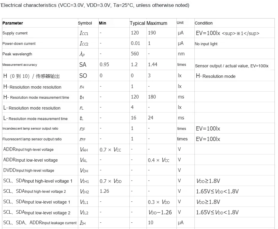
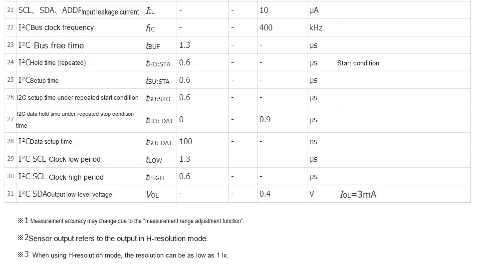
The descriptions of some parameters in the above table are as follows:
- Supply current: typically 120μA during operation (
EV= 100lx), typically 0.01μA in power-down mode (no input light), featuring low power consumption. - Measurement Performance:
- Peak wavelength: 560nm, measurement accuracy: 0.95~1.44 times (
EV= 100lx); - H - resolution mode with a resolution of 1 lx and a measurement time of 120~180 ms; L - resolution mode with a resolution of 4 lx and a measurement time of 16~24 ms.
- Peak wavelength: 560nm, measurement accuracy: 0.95~1.44 times (
- Input level:
ADDR,SCL,SDAhave different thresholds for high/low input levels depending on theVCCandVDDranges to ensure effective signal identification. - Input leakage current:
SCL,SDA,ADDRhave a maximum input leakage current of 10μA and low quiescent current.
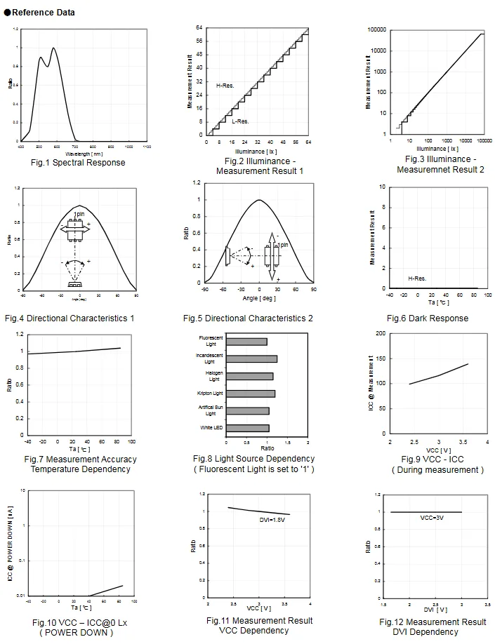
BH1750 is a digital ambient light intensity sensor, and its core performance parameters can be summarized from the figure as follows:
- Spectral Response: The peak wavelength is approximately 560 nm, which is close to the human visual characteristics and can simulate the human eye's perception of light;
- Illuminance measurement: It features a wide measurement range (supporting illuminance as low as 1 lx and as high as 100000 lx), with an output that exhibits an excellent linear relationship with illuminance, making it adaptable to different brightness scenarios;
- Direction/Angle Adaptability: It exhibits relatively stable response to the incident direction and angle of light, with minimal fluctuation in measurement results across different incident angles;
- Environmental compatibility: It exhibits weak temperature dependence (minimal variation in measurement accuracy across different temperatures) and high response consistency to different light sources such as fluorescent and incandescent lamps, making it adaptable to a wide range of lighting environments;
- Power Supply and Power Consumption: Wide operating voltage range (typically 2.5V~3.5V), operating current during measurement is only a few mA, extremely low current in power-down mode, and low power consumption;
- Measurement accuracy: High resolution (supports high-precision measurement at the 0.5 lx level), outputs digital signals without requiring additional
ADconversion.
2.5 Reference Circuit
None.
2.6 Chip Configuration
2.6.1 Turn on the VCC power supply
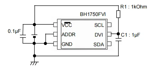
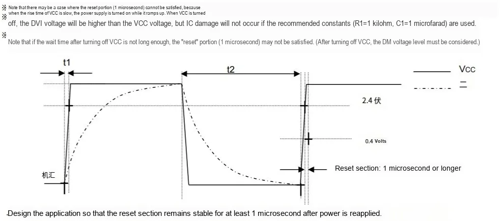
BH1750FVI-TR requires attention to the power-up sequence of VCC and DVI during use, the detailed description is as follows.
VCCandDVIPower Supply Recommended Sequence Diagram
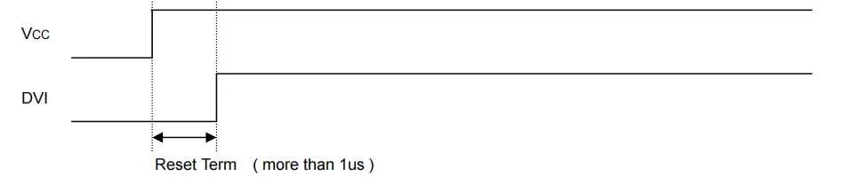
In the Sequence Diagram, VCC rises first, then DVI rises, and the " Reset Term " duration between the rising edges of the two must exceed 1 μs.
VCCandDVIPower Sequence Diagram 2 (ifDVIrises within 1 μs afterVCCis powered on)
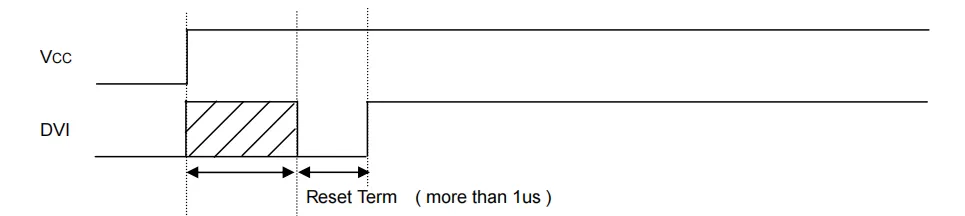
After the VCC rises in the Sequence Diagram, the DVI rises within 1μs, and the " Reset Term " time after the DVI rises needs to exceed 1μs. The twill area before the DVI rises is in the "irrelevant state" - If the system does not provide the "1" level duration of the DVI (1μs), the ADDR , SDA , and SCL states are unstable .
Note: In this case, please connect a resistor (approx. 100kΩ) to ADDR instead of connecting it directly to VCC or GND, as it is a tri-state buffer for internal testing purposes.
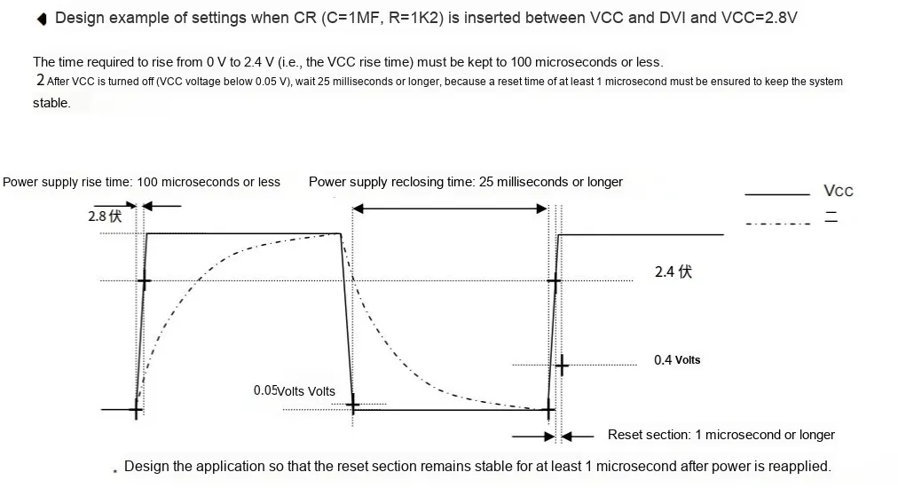
2.6.2 Turn off the VCC power supply
Insert a low-pass filter (LPF) using CR between VCC and DVI. This method may not meet the reset requirements at power-on.
2.7 Communication Interfaces and Related Protocols
2.7.1 I2C Bus Communication
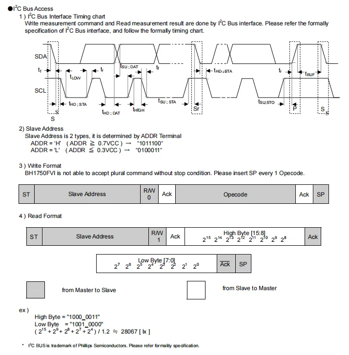
BH1750 I²C bus communication protocol, which is used to realize command interaction and data reading between the master and the BH1750:
- Communication method: Both writing measurement commands and reading measurement results are completed via the
I²Cbus, and the standardI²Ctiming requirements shall be followed; - Slave address: determined by the level of the
ADDRpin; whenADDRis pulled high (≥0.7VCC), it corresponds to the address "1011100", and when pulled low (≤0.3VCC), it corresponds to "0100011"; - Write Format: A single write operation shall be performed in the sequence "Start → Slave Address (
RW= 0) → Acknowledge → Opcode → Acknowledge → Stop", and commands shall not be sent consecutively (a stop bit must be added after each opcode); - Reading Format: The reading process is "Start → Slave Address (
RW= 1) → ACK → Receive High Byte → ACK → Receive Low Byte → ACK → Stop", and the final illuminance value is calculated by "(High Byte + Low Byte)/1.2"(unit: lx).
2.7.2 Adjust the measurement results to eliminate the influence of the optical window (sensor sensitivity adjustment)
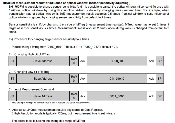
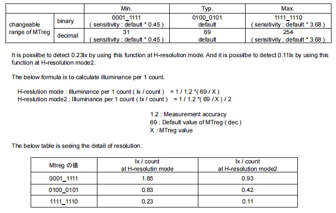
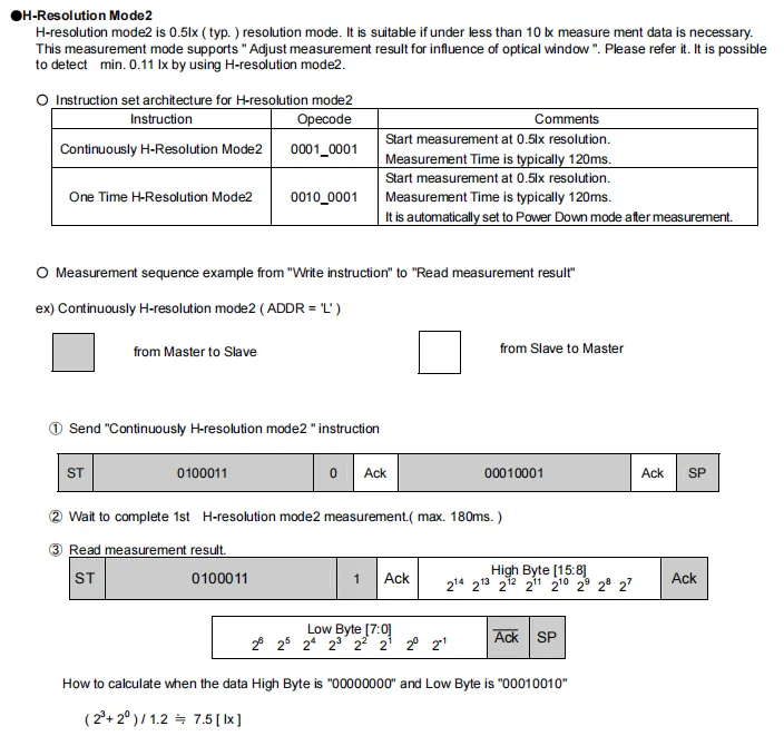
This section describes BH1750 's sensor sensitivity adjustment and H-Resolution Mode2 (High Resolution Mode 2) function:
- Sensitivity adjustment: Used to compensate for the light transmission impact of the optical window (for example, when the window transmittance is 50%, the sensitivity can be adjusted to 2 times to offset the error), which is realized by modifying the high and low bits of the measurement time register (
MTreg) — first write the high and low bit values ofMTregtwice in sequence (for example, to change the default value to 2 times, write "1000_100" and "011_010"), then send a measurement command, at this time the measurement time will change synchronously with the value ofMTreg(default 120ms → 240ms). Different values ofMTregcorrespond to different sensitivity multiples, and will also affect the illuminance resolution. H-Resolution Mode2: A low-illumination mode with a resolution of 0.5 lx (typical value), adapted for scenarios <10 lx, supporting optical window compensation, and covering two commands: "continuous measurement" and "single measurement(automatic power-off after completion)". The measurement process is as follows: send the corresponding mode command → wait for up to 180 ms → read the high and low byte data, and the final illuminance value is calculated as "(high byte + low byte)/1.2"(unit: lx).
2.8 PCB Routing Precautions
BH1750FVI-TR does not come with PCB layout instructions.
III. Circuit Engineering
3.1 Circuit Source Engineering
To obtain the source project of the circuit, please follow the official account [Freak Embedded]
3.2 Module Usage Instructions
SCH_Schematic1_BH1750-Based Light Intensity Sensor-V1.0_2025-11-12.pdf 2.0 MB
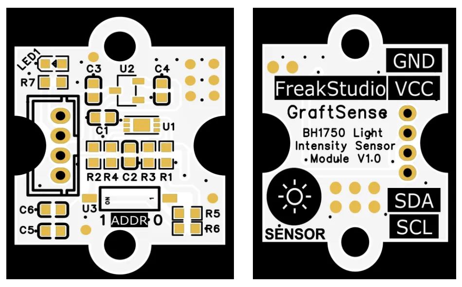
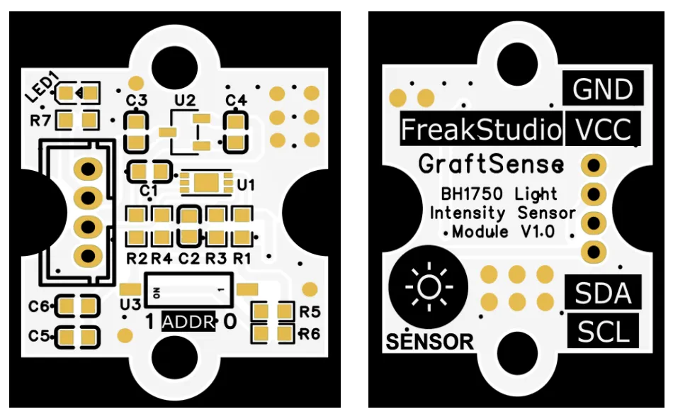
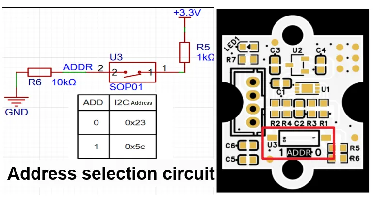
This module provides an I2C communication interface: it supports standard I2C communication rates; by selecting 0/1 via the ADDR pin on the module, two 0100011 and 1011100 I2C addresses can be configured, it is compatible with 3.3V/5V logic levels, and can stably transmit the digitalized ambient light intensity data within the range of 1~65535 detected by BH1750. It is applicable to scenarios such as light collection for maker projects, automatic brightness adjustment for smart homes, dimming control for device displays, etc. , and provides accurate ambient light data interaction capability for the system.
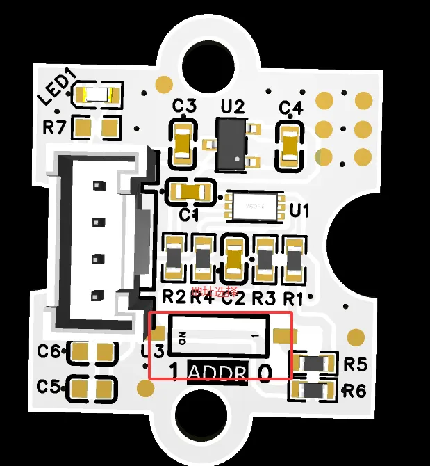
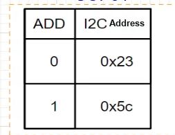
The module's IIC address can be controlled by adjusting the DIP switches; for the correspondence between DIP switch positions and address selection, please refer to the following figure.
3.3 Application Experiment
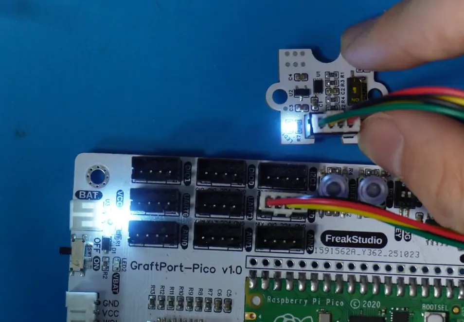
Here, we use the GraftPort-RP2040 development board for testing, and connect the light intensity sensor module based on the BH1750 chip to communicate with the main controller via the I2C interface.
Here, we first use the HY2.0-4P connection cable to connect the module to the GraftPort-RP2040 development board's I2C0 interface:
Here, we need to set the address bits in advance via the DIP switch:(the selected address is 0x5C)
The module connections are shown in the following table:
Development Board Pins | Module Pins | Description |
Pin 4 |
| I2C data transmission line, corresponding to |
Pin 5 |
| I2C clock signal line, corresponding to |
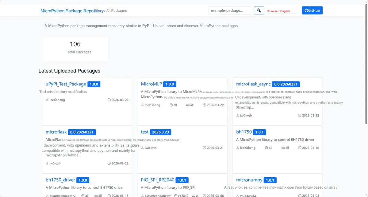
Here, we need to search for the relevant driver packages on uPyPI: https://upypi.net/zh/
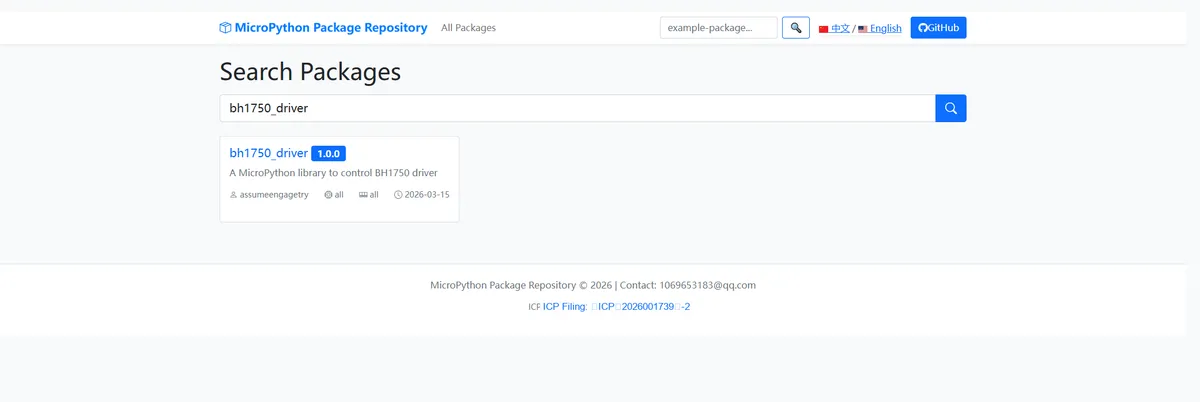
Enter bh1750_driver to search, and the following will be displayed:
Click to copy the local installation command:
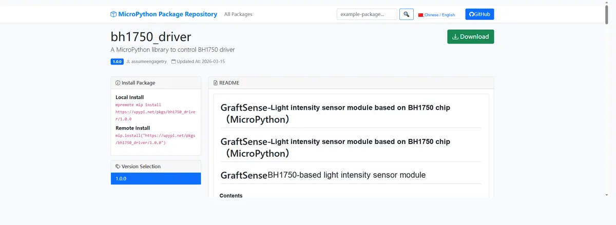
Here, we can use the mip tool to import module driver library code. Below are the usage commands for the mpremote tool:
mpremote mip install github:FreakStudioCN/GraftSense-Drivers-MicroPython/sensors/bh1750_driverImport the light intensity sensor module based on BH1750 chip - MicroPython test code, then copy the following main.py code into our project:
# Python env   : MicroPython v1.23.0
# -*- coding: utf-8 -*-
# @Time    : 2025/09/04 10:00
# @Author  : 侯钧瀚
# @File    : main.py
# @Description : PCA9685 16-channel PWM driver board example program

# ======================================== Import Modules =========================================

# Import the time module
import time
# Import MicroPython standard library modules
from machine import Pin, I2C
# Import the bus servo controller module
from bus_servo import BusPWMServoController
# Import the PCA9685 module
from pca9685 import PCA9685

# ======================================== Global Variables ============================================

# Automatically scan for the PCA9685 address (0x40~0x4F)
addr = 0x40

# ======================================== Functions ============================================

# ======================================== Custom Classes ============================================

# ======================================== Initialization ==========================================

# Power-on delay of 3 s
time.sleep(3)
# Print debug message
print("FreakStudio: Using PCA9685 to control the angles of two servos")
# Create a hardware I2C instance using the I2C0 peripheral, with a clock frequency of 400KHz, SDA pin 4, and SCL pin 5
i2c = I2C(id=0, sda=Pin(4), scl=Pin(5), freq=400000)

# Start scanning for devices on the I2C bus and return a list of slave addresses
devices_list = i2c.scan()
print('START I2C SCANNER')

# If devices_list is empty, no device is connected to the I2C bus
if len(devices_list) == 0:
    print("No i2c device !")
# If not empty, print the slave device addresses
else:
    print('i2c devices found:', len(devices_list))
    # Iterate over the slave device address list
    for device in devices_list:
        # Check whether the device address is the PCF8575 address
        if device >= 0x40 and device <= 0x4F:
            print("I2C hexadecimal address: ", hex(device))
pca = PCA9685(i2c,  address = device)

# Create the controller (50Hz is commonly used for servos)
srv = BusPWMServoController(pca, freq=50)

# Bind servo channels

# Channel 0: 180° servo, standard 500~2500us, 1500us is neutral
srv.attach_servo(0, BusPWMServoController.SERVO_180, min_us=500, max_us=2500, neutral_us=1500)
# Channel 1: 180° servo, standard 500~2500us, 1500us is neutral
srv.attach_servo(1, BusPWMServoController.SERVO_180, min_us=500, max_us=2500, neutral_us=1500)
# Channel 2: 180° servo, standard 500~2500us, 1500us is neutral
srv.attach_servo(2, BusPWMServoController.SERVO_180, min_us=500, max_us=2500, neutral_us=1500)
# Channel 3: 180° servo, standard 500~2500us, 1500us is neutral
srv.attach_servo(3, BusPWMServoController.SERVO_180, min_us=500, max_us=2500, neutral_us=1500)

# Set the 360° servo channels
# Channel 1: 360° continuous servo, with its own stop point near 1500us; use reversed=True for reverse direction if needed
srv.attach_servo(4, BusPWMServoController.SERVO_360, min_us=1000, max_us=2000, neutral_us=1500)
# Channel 1: 360° continuous servo, with its own stop point near 1500us; use reversed=True for reverse direction if needed
srv.attach_servo(5, BusPWMServoController.SERVO_360, min_us=1000, max_us=2000, neutral_us=1500)

# ========================================  Main Program  ===========================================

# Demonstrate 180° angle control
# Turn to 0°
srv.set_angle(0, 0.0)
# Turn to 0°
srv.set_angle(1, 0.0)
# Turn to 0°
srv.set_angle(2, 0.0)
# Turn to 0°
srv.set_angle(3, 0.0)
time.sleep(1)
# Smoothly turn to 90° at about 120°/s
srv.set_angle(0, 90.0, speed_deg_per_s=120)
# Smoothly turn to 90° at about 120°/s
srv.set_angle(1, 90.0, speed_deg_per_s=120)
# Smoothly turn to 90° at about 120°/s
srv.set_angle(2, 90.0, speed_deg_per_s=120)
# Smoothly turn to 90° at about 120°/s
srv.set_angle(3, 90.0, speed_deg_per_s=120)
time.sleep(1)
# Smoothly turn to 180°
srv.set_angle(0, 180.0, speed_deg_per_s=180)
# Smoothly turn to 180°
srv.set_angle(1, 180.0, speed_deg_per_s=180)
# Smoothly turn to 180°
srv.set_angle(2, 180.0, speed_deg_per_s=180)
# Smoothly turn to 180°
srv.set_angle(3, 180.0, speed_deg_per_s=180)
time.sleep(1)
# Return to center or stop
srv.stop(0)

# Demonstrate 360° speed control
# Clockwise at medium speed
srv.set_speed(4, +0.6)
# Clockwise at medium speed
srv.set_speed(5, +0.6)
time.sleep(20)
# Reverse at medium speed
srv.set_speed(4, -0.6)
# Reverse at medium speed
srv.set_speed(5, -0.6)
time.sleep(20)
# Channel 4 returns to center or stops
srv.stop(4)
# Channel 5 returns to center or stops
srv.stop(5)
# Return to center or stop

time.sleep(0.5)
# Turn off output and unbind
srv.detach_servo(0)
# Turn off output and unbind
srv.detach_servo(1)
# Turn off output and unbind
srv.detach_servo(2)
# Turn off output and unbind
srv.detach_servo(3)
# Turn off output and unbind
srv.detach_servo(4)
# Turn off output and unbind
srv.detach_servo(5)
This code is a test program for the BH1750 illuminance sensor written in MicroPython. It first initializes the I2C bus, scans and identifies the BH1750 I2C device address, creates a sensor instance, and then tests the three measurement modes in sequence:
- First, read the illumination values 5 times in single measurement mode
- Then switch to the continuous measurement mode and take 5 readings
- Finally, reading is performed 5 times through the generator pattern to complete the verification of illumination Data Acquisition under different modes.
Burn the code, open the terminal, and use the mpremote tool to connect to the main controller. The output is as follows:
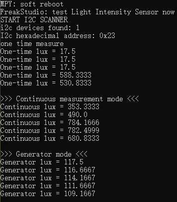
The terminal output shows that I2C scan successfully found the 0x23 address BH1750 device:
It can be seen that in a single measurement, the illumination value is low at the initial stage and then rises sharply; in the continuous measurement mode, the value keeps increasing; while in the generator mode, the value decreases slightly and then tends to be stable. This not only indicates that the sensor can normally collect illumination data in all three modes, but also reflects that the ambient illumination changed during the test, and the response of the sensor meets the functional expectation.
IV. Drivers
bh1750_driver.zip 11 KB
5. BOM & Recommended Alternative Parts
None.
VI. Revision History
Document Version | Date of Revision | Modifier | Modified Content |
v1.0 | 2025-11-12 | Ling Gaoxing | Initialize the document |
v1.1 | 2025-12-29 | Li Zisheng | Added application experiments and production files |
v1.2 | 2025-12-31 | Xin Ruili | Create an open version of the document based on the internal document version v1.1. |
v1.3 | 2026-03-29 | Xin Ruili | Modified the application experiment section |
VII. Relevant Materials
7.1 Chip Datasheet
BH1750.pdf 545 KB
7.2 Unique Icons for PCB Silkscreen