Contents
- I. Module Introduction
- II. Introduction to Major Chips
- 2.1 Chip Overview
- 2.2 Pin Definition
- 2.3 Functional Block Diagram
- 2.4 Performance Parameters
- 2.5 Reference Circuit
- 2.6 Chip Configuration
- 2.7 Communication Interfaces and Related Protocols
- 2.8 PCB Routing Precautions
- III. Instructions for Circuit Engineering and Module Usage
- 3.1 Circuit Source Engineering
- 3.2 Module Usage Instructions
- 3.3 Application Experiment
- IV. Drivers
- 5. BOM & Recommended Alternative Parts
- VI. Revision History
- VII. Relevant Materials
- 7.1 Chip Datasheet
- 7.2 Unique Icons for PCB Silkscreen
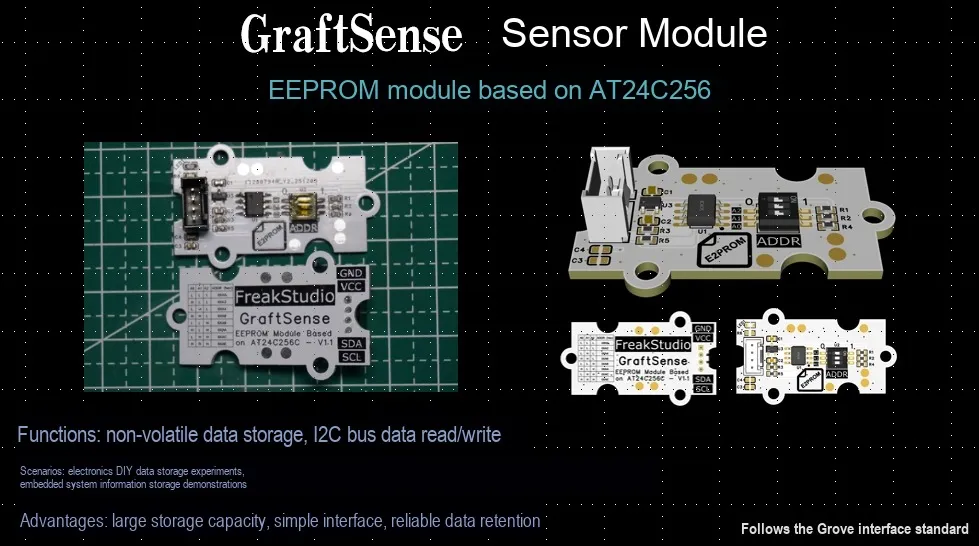
I. Module Introduction
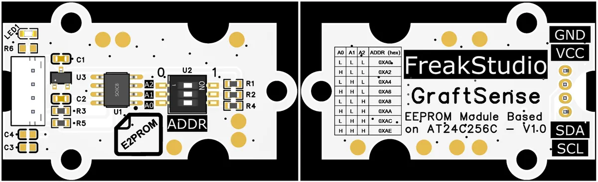
EEPROM Module Based on AT24C256 Designed based on the AT24C256C chip, it supports I2C communication (via SDA and SCL interfaces), integrates a DC-DC 5V-to-3.3V circuit and an address selection DIP switch (supports configurable multiple I2C addresses). Featuring non-volatile data storage capability, it is applicable to scenarios such as maker development and industrial control, providing a reliable long-term data storage solution for devices.
II. Introduction to Major Chips
External EEPROM chips are a common type of non-volatile memory device, often used in embedded systems to store parameters such as system configuration and calibration data, with storage capacities ranging from a few Kbits to several Mbits. We commonly use the I2C protocol to communicate with external EEPROM chips, which feature the ability to retain data after power-off and support individual read/write operations for any byte;EEPROM offers fast read speeds, typically ranging from tens to hundreds of nanoseconds, but has a relatively slow write speed, generally from a few milliseconds to tens of milliseconds, and its erase-write endurance usually ranges from 100,000 to 1 million cycles.
Compared with external Flash chips, external EEPROM chips feature smaller capacity and slower write speed, but they support independent erasure and writing of individual bytes with a high write cycle count, making them suitable for storing small data that requires frequent updates.
Here, it is necessary to distinguish between the units Kbit (kilobit) and KB (kilobyte): 1 Kbit = 1000 bits, while 1 KB = 1024 bytes. Since one byte equals eight bits, 1 KB = 8 Kbit.
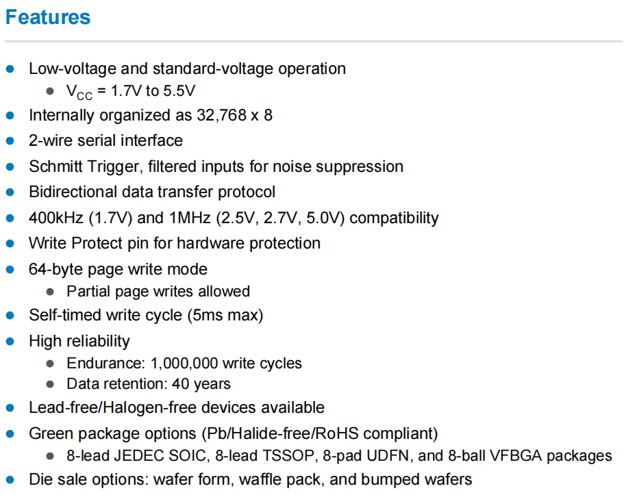
The AT24CXX series of chips are manufactured by Microchip Technology and are EEPROM chips that feature an I2C interface, support multi-master mode, and facilitate easy communication with microcontrollers. They also operate over a wide supply voltage range from 1.7V to 5.5V, supporting both low-voltage and standard-voltage operation: at 1.7V, they support a maximum communication rate of 400kHz, while at 2.5V, 2.7V and 5.0V, the maximum supported communication rate can reach 1MHz.
2.1 Chip Overview
The following is the AT24C256 chip we commonly use, with a capacity of 256 Kbit:
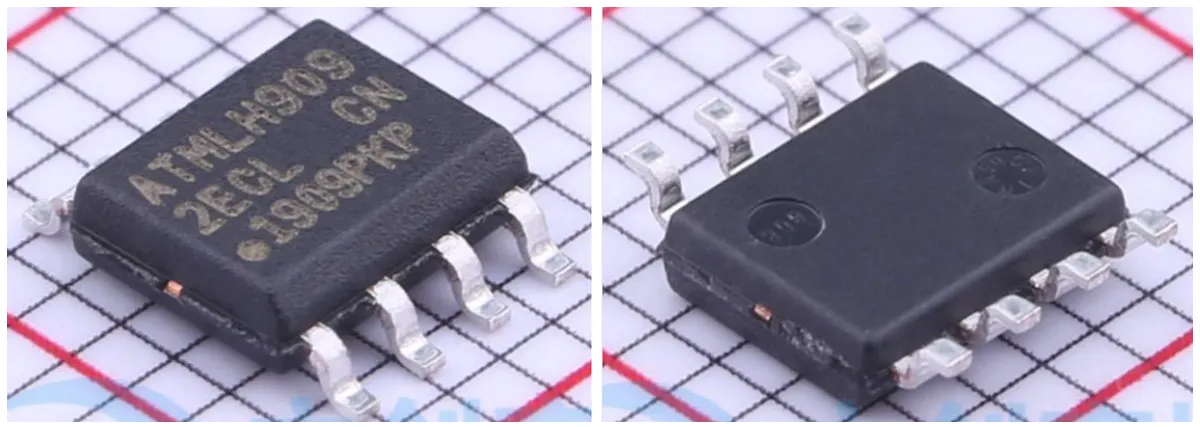
AT24C256 The chip also has the following features:
- Noise Suppression: Built-in Schmitt trigger and filtered inputs enhance anti-interference capability;
- Write-protect pin: provides hardware protection against accidental writing;
- Self-timed write cycle: the maximum write time is 5 milliseconds;
- High reliability: with write cycle endurance up to 1,000,000 cycles and data retention time up to 40 years.
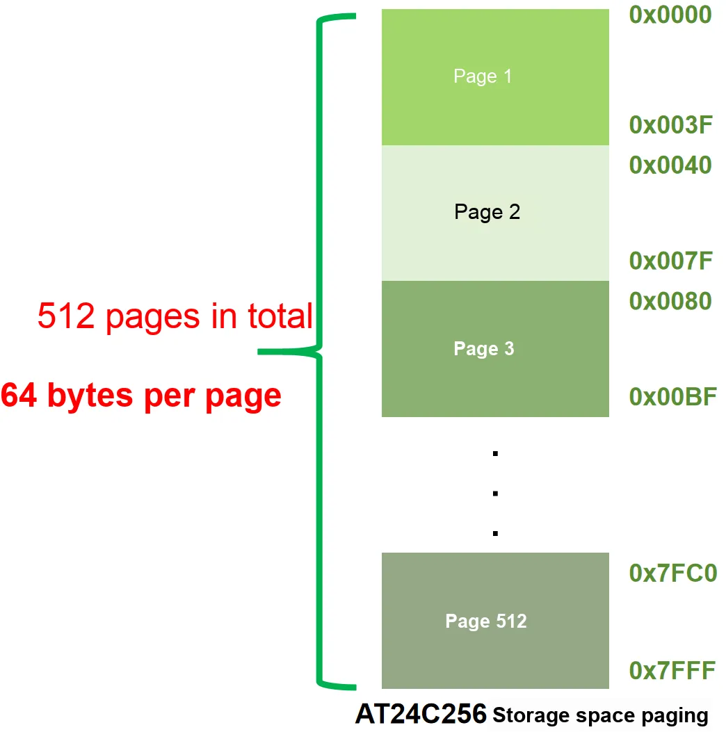
Here, the AT24C256 chip divides its 256-Kbit storage space into 512 pages, each containing 64 bytes. The address range of the first page is 0x0000~0x003F, and the remaining space is evenly divided into the following 512 pages in sequence, as shown in the figure below:
AT24C256 chip supports two write modes: page write and partial page write.
- Page Write: A complete page (typically 64 bytes) is written to
EEPROMin a single operation. During a page write, all data must be written to the page; if only partial data needs to be written, the remaining portion of the page will be overwritten with the new data. Page writes are generally fast. - Partial page write: It allows selectively writing a small amount of data within a single page without overwriting the entire page. Users can update only some bytes in the page while leaving the rest unchanged, which is extremely useful for data that requires frequent updates to specific bytes. However, partial page writes are relatively slow.
2.2 Pin Definition
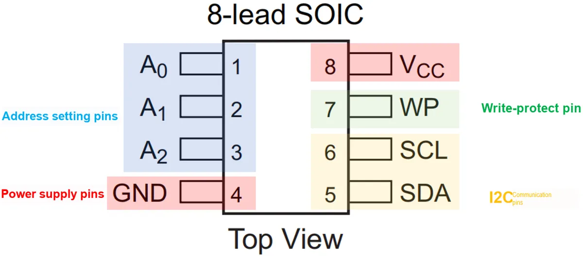
AT24C256 The pin names and functions of the chip are as follows:
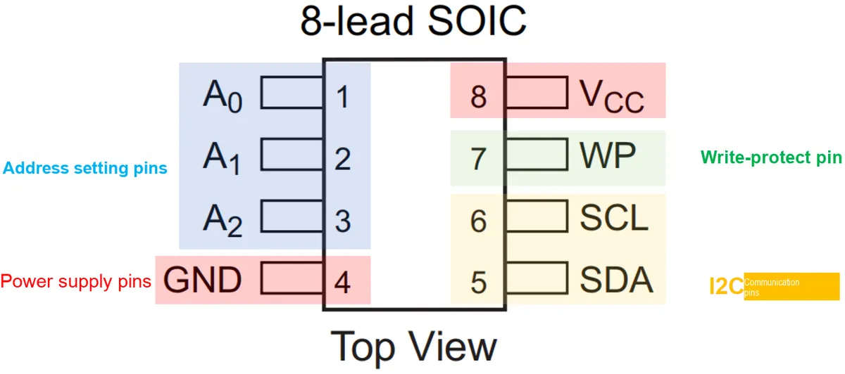
Among them, A2, A1 and A0 pins are device address inputs, which can be connected to GND or VCC to set the address of the AT24C256 chip. If these pins are floating (i. e., not externally connected to GND or VCC), A2, A1 and A0 pins will be internally pulled low to GND; here, when A2, A1 and A0 are connected to VCC via pull-up resistors, it is recommended that the resistance value of the pull-up resistors be less than 10kΩ.
AT24C256 The communication address setting of the chip is as follows:
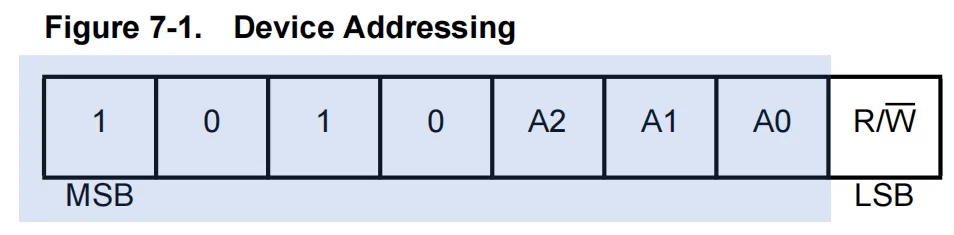
Among these bits, the first four are fixed as 1010, which is the universal standard for 2-wire EEPROM devices, while the following three bits correspond to the device's address input pins A2, A1 and A0; by connecting these address input pins to VCC or GND, up to eight such devices can be connected to the same bus.
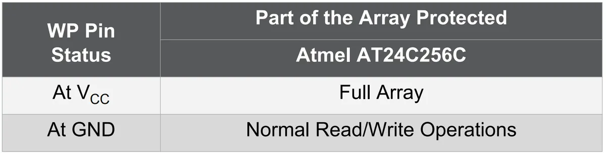
WP pin is a write-protect input pin. When connected to GND, normal write operations are permitted; when connected to VCC, all write operations will be disabled. If this pin floats, the WP pin will be internally pulled low to GND. When the WP pin is connected to VCC via a pull-up resistor, it is recommended that the resistance of the pull-up resistor be less than 10kΩ.
2.3 Functional Block Diagram
The following is the internal structure of the AT24C256C chip:
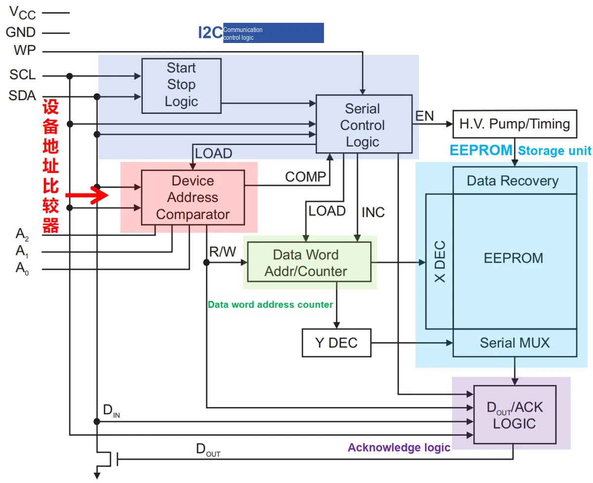
It includes the following parts:
I2Ccommunication control logic: used to handleI2Cbus start and stop conditions, as well as manage and coordinate various control signals during data transmission;- Device Address Comparator: It checks whether the incoming device address matches the internally set address to determine whether to respond to the host's commands;
EEPROMmemory cell: consisting of a data recovery unit, a memory cell and a data selection unit; the data recovery unit is configured to handle potential data corruption or loss that may occur during the write process, data access takes place in the actual memory cell, and the data selection unit is configured to select data among multiple data channels;- Data Word Address Counter: It is used to track the current data address or data word to ensure the correct reading and writing of data;
- Response Logic: responsible for outputting data from
EEPROMto the host and processing response signals.
2.4 Performance Parameters
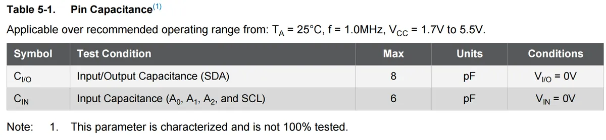
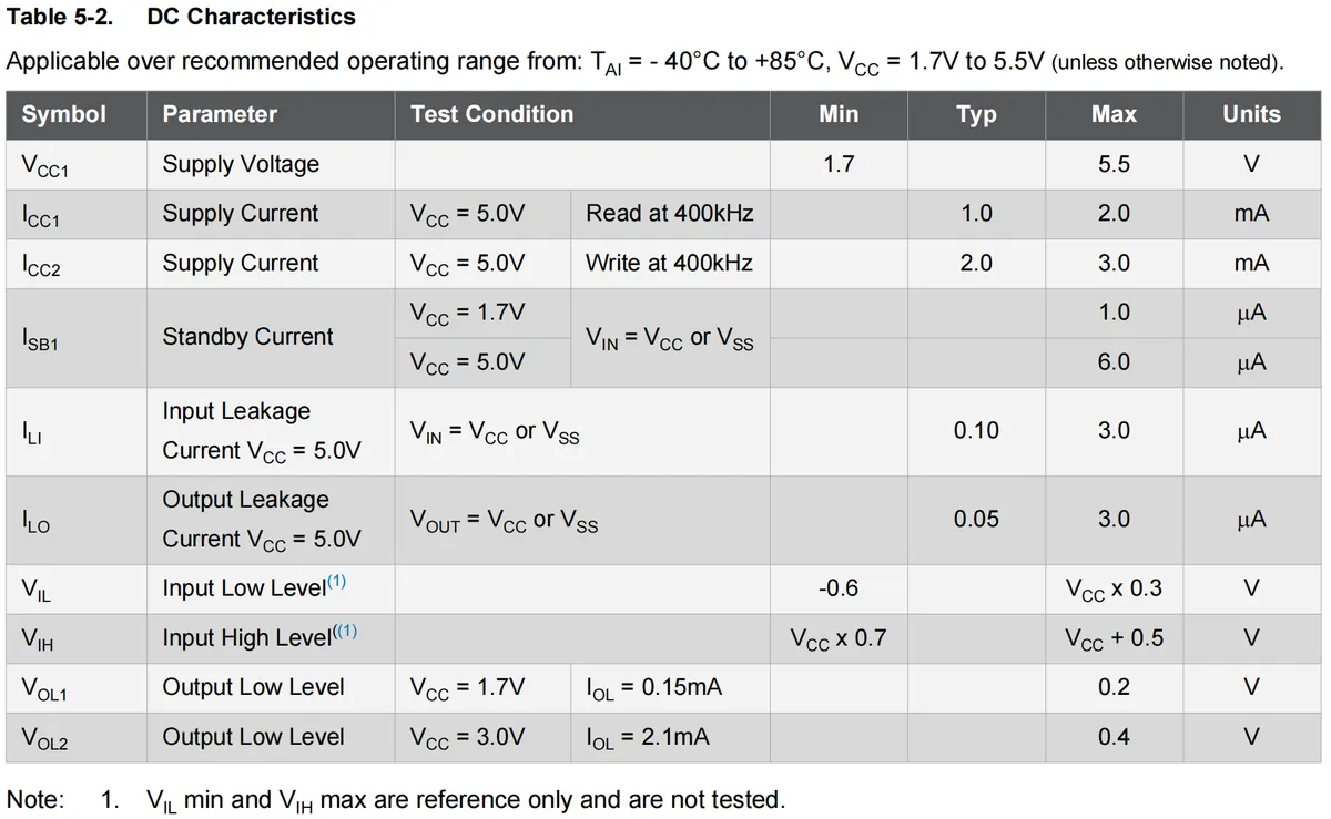
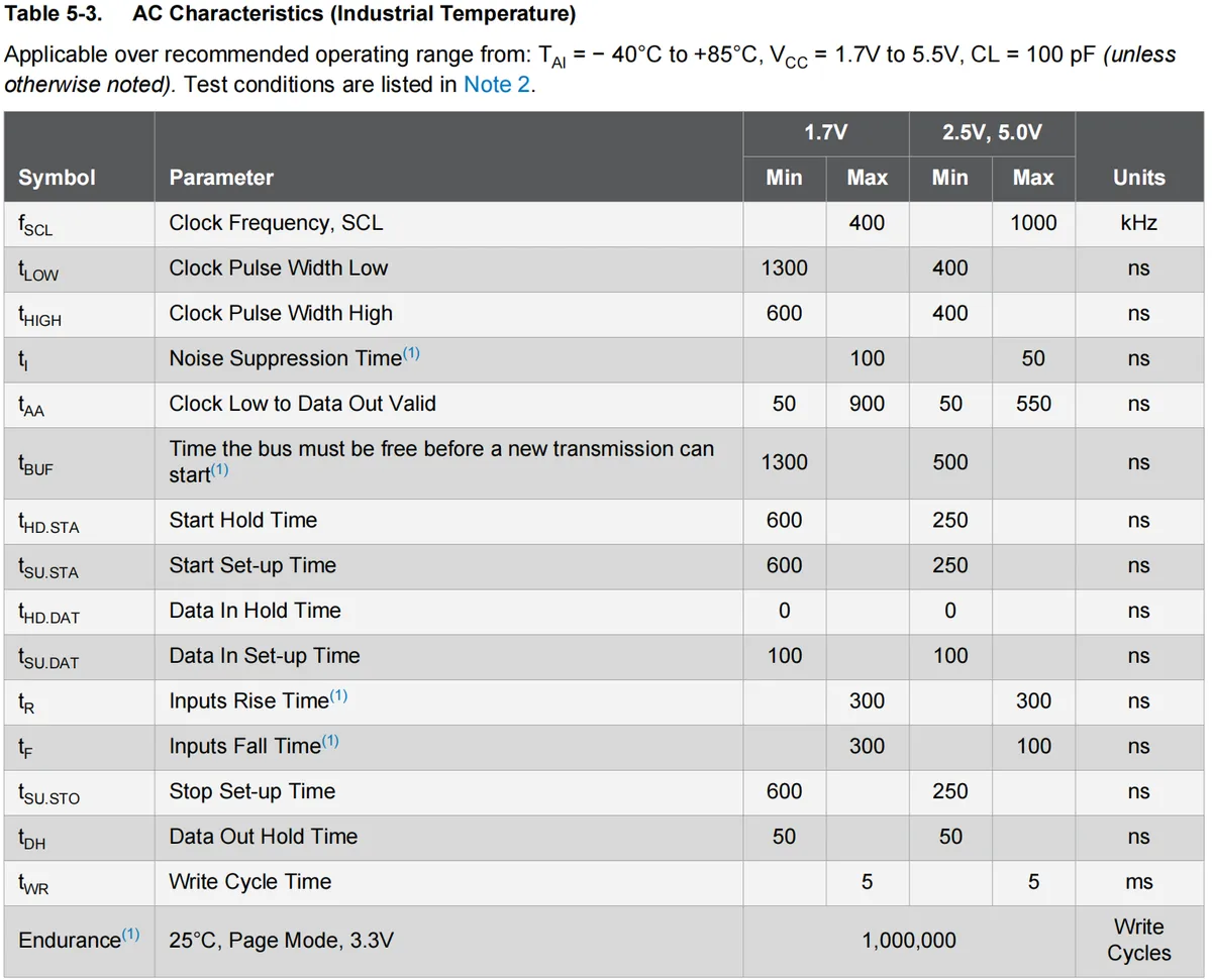

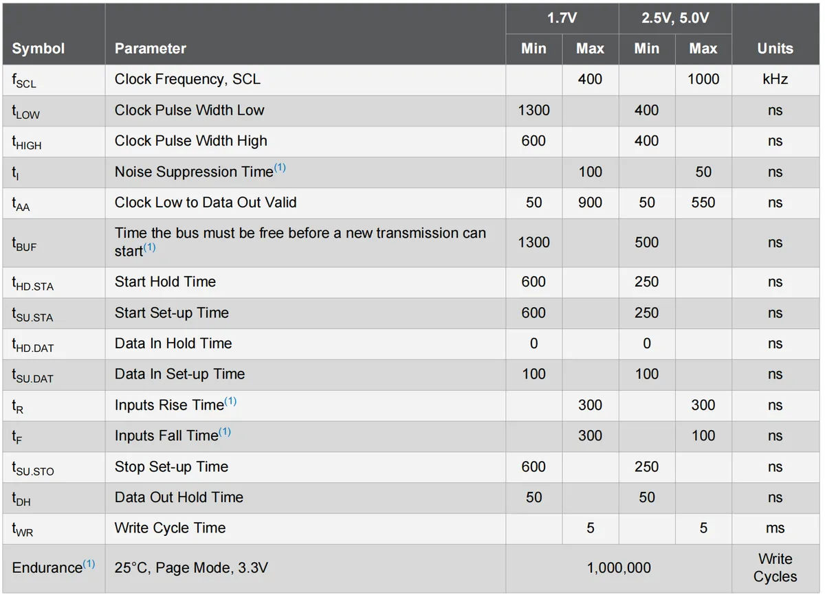
SCL and SDA are I2C communication pins. For the electrical parameters of I2C protocol communication, please refer to the datasheet:
2.5 Reference Circuit
None.
2.6 Chip Configuration
We can configure the address of the A2, A1 and A0 pins to connect to GND or VCC to set the address of the AT24C256 chip.
2.7 Communication Interfaces and Related Protocols
AT24C256C chip communicates via the I2C communication interface.
2.7.1 Chip Data Writing
Next, let's walk through the data read/write process of the AT24C256 chip. First, we will cover the data write operation of the AT24C256 chip. Here, the AT24C256C supports two write modes: Byte Write and Page Write.
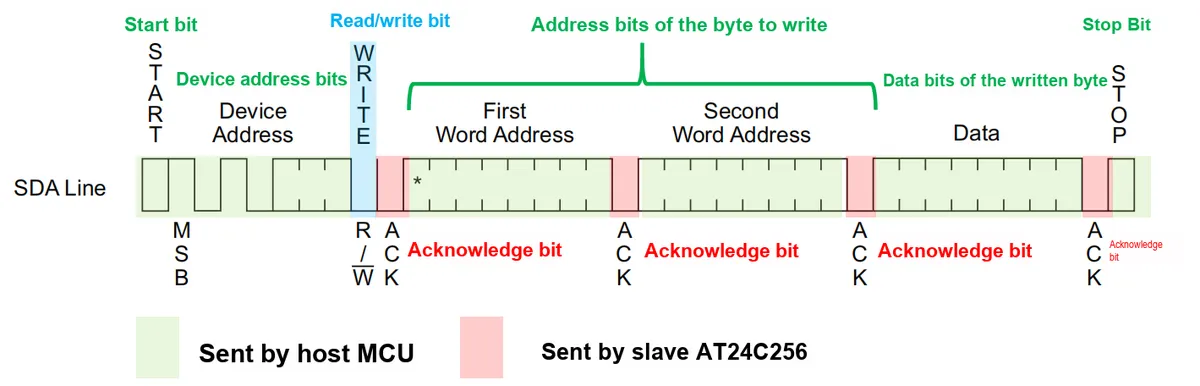
- Byte Write (
Byte Write): This mode supports writing one byte of data to any address. The microcontroller first sends a "start condition" signal, then sends the device address; after these two signal transmissions,AT24C256Cwill send an acknowledgeACKsignal;Next, the microcontroller sends two address bytes to specify the memory location to be written, and after waiting for the acknowledge signal fromAT24C256C, the microcontroller subsequently sends an 8-bit data word. After receiving the data,AT24C256Cresponds with another acknowledge signal to indicate that the data has been received successfully. Finally, the microcontroller sends a "stop condition" signal to terminate the write operation.
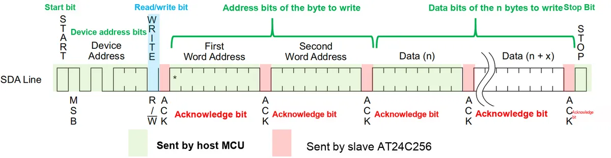
- Page Write (
Page Write): Similar to byte write, the microcontroller first sends a start signal, the device address bits, and the two address bytes of the first word to be written, then the microcontroller sends the first data word; after that, the microcontroller can continue to send up to 63 data words without sending a stop signal each time.The AT24C256chip will return an acknowledge signal after receiving each data word. When all data has been sent, the microcontroller finally sends a stop signal to terminate the page write operation.
Here, AT24C256 requires two address bytes since its storage capacity reaches 256 Kbit; the address space of one byte (8 bits) can only represent 2^8 = 256 addresses, whereas AT24C256 has 256 Kbit = 32 KB = 32768 bytes, which requires 2^15 = 32768 addresses for full addressing. Therefore, two address bytes need to be sent during writing; 16 address bits can represent 2^16 = 65536 addresses, where the first address byte is typically used to indicate the upper 8 bits of the address, and the second address byte is used to indicate the lower 8 bits of the address.
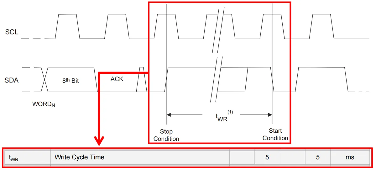
After AT24C256 starts a write operation (such as byte write or page write), the microcontroller cannot immediately perform the next operation on the AT24C256 chip, because the AT24C256 is processing the write. At this point, we can continuously use the microcontroller to send a start signal, device address bits, and read/write signal to wait until the AT24C256 finishes the write, after which it will return an acknowledge signal. We can use this method to determine whether the AT24C256 chip has completed the write operation.
It should also be noted that AT24C256 has a write timing requirement that a delay of tWR must be added after each data communication is completed to ensure that the EEPROM finishes the write operation, so as to avoid data loss or errors. The value of tWR can be found in the I2C communication electrical parameters section of the datasheet:
2.7.2 Chip Data Reading
For data reading of AT24C256, it can be divided into three modes: Current Address Read, Random Read and Sequential Read.
- Current Address Read (
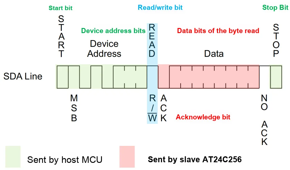
Current Address Read): This mode is used to read the data at the current address retained after the last operation. The microcontroller sends a start signal, a device address, and a read/write bit (set to 1).AT24C256will respond with an acknowledge signal after receiving the device address, and thenAT24C256will output the data word sequence at the current address to the microcontroller. The current address is the address retained after the last read or write operation, and this address is automatically incremented by 1 after the reading is completed. After receiving the data, the microcontroller does not need to return an acknowledge signal, but directly sends a stop signal to terminate the read operation.
- Random Read (
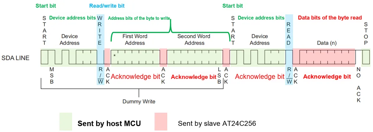
Random Read): This method is used to read a specific byte of data at a designated address. The microcontroller first sends a start signal and the device address, then performs a "dummy write operation" with the read/write bit set to 0; this operation essentially transmits the address of the data word to be read toAT24C256.AT24C256will send an acknowledge signal upon receiving the address, after which the microcontroller needs to send another start signal followed by the device address with the read/write bit set to 1.AT24C256will respond with an acknowledge signal after receiving the new device address, and output the data byte corresponding to the target address.
- Sequential Read (
Sequential Read): This method is used to read data consecutively starting from a certain address; during the reading process, the address will automatically increment until it reaches the last address, after which the address will wrap around to the first one, and the specific communication process is similar to the read operation described above.
2.8 PCB Routing Precautions
None.
III. Instructions for Circuit Engineering and Module Usage
3.1 Circuit Source Engineering
To obtain the source project of the circuit, please follow the official account [Freak Embedded]
3.2 Module Usage Instructions
The schematic diagram of this module is shown below:
SCH_AT24C256C-Based_EEPROM_Module_v1.0_2025-11-23.pdf 2.0 MB
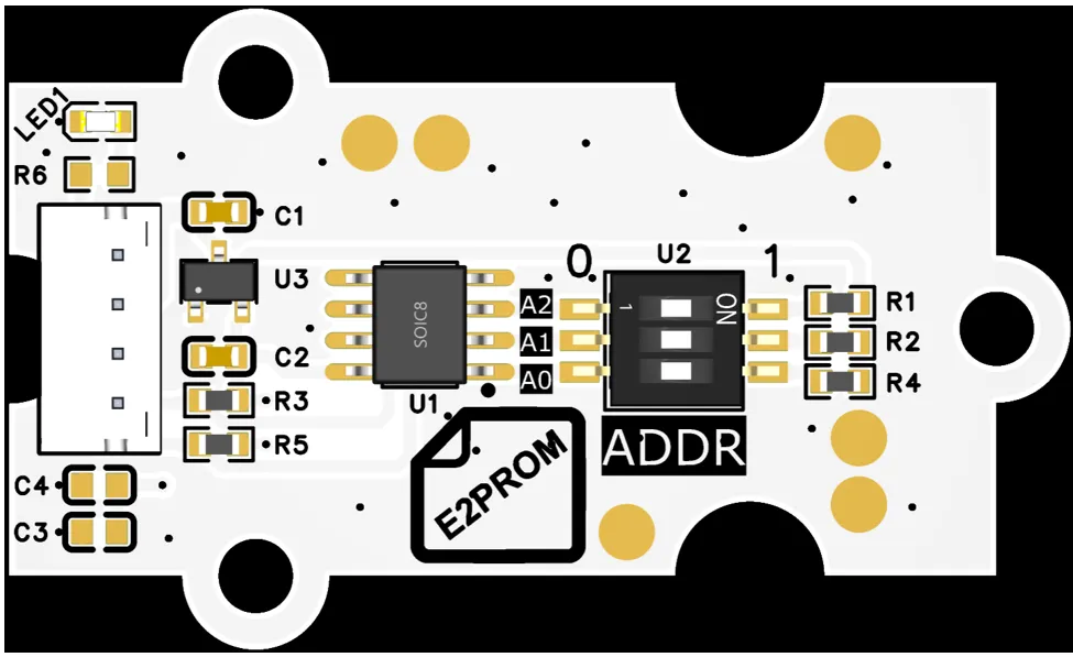
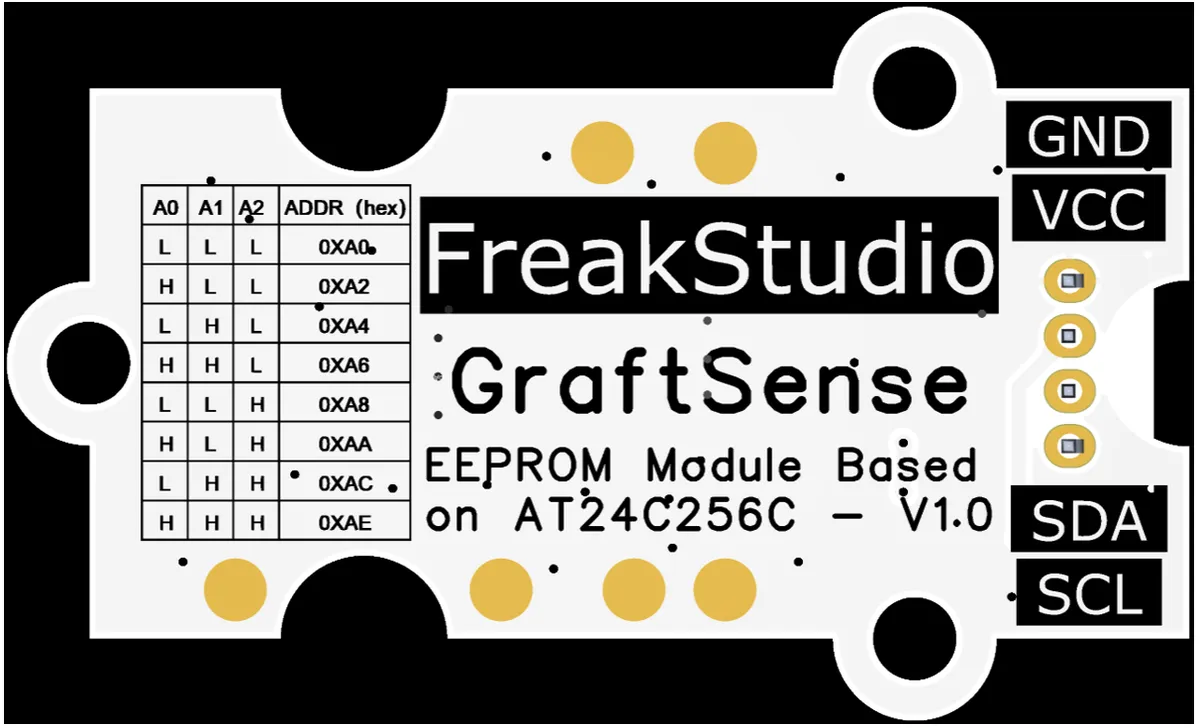
This module provides an I2C communication interface: it supports standard I2C communication baud rates, and can flexibly configure multiple A0, A1, and A2 DIP switches to flexibly configure various I2C addresses (such as 0xA0, 0xA2, etc.), is compatible with 3.3V/5V logic levels, and can stably implement read and write operations for 256Kbit (32KB) non-volatile data. It is suitable for scenarios such as parameter storage for maker projects and configuration information backup for industrial equipment, providing the system with reliable long-term data storage and interaction capabilities.
3.3 Application Experiment
Here, we use the GraftPort-RP2040 development board for testing, and the EEPROM module based on AT24C256C uses the I2C interface to communicate with the main controller.
Here, we need to set the address bits in advance via the DIP switch: the address selected in the application experiment is 0xA0
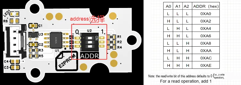
Here, we use the HY2.0-4P cable to connect the module to the GraftPort-RP2040 development board's I2C0 interface:
The module connections are shown in the following table:
Development Board Pins | Module Pins | Description |
Pin 4 |
|
|
Pin 5 |
|
|
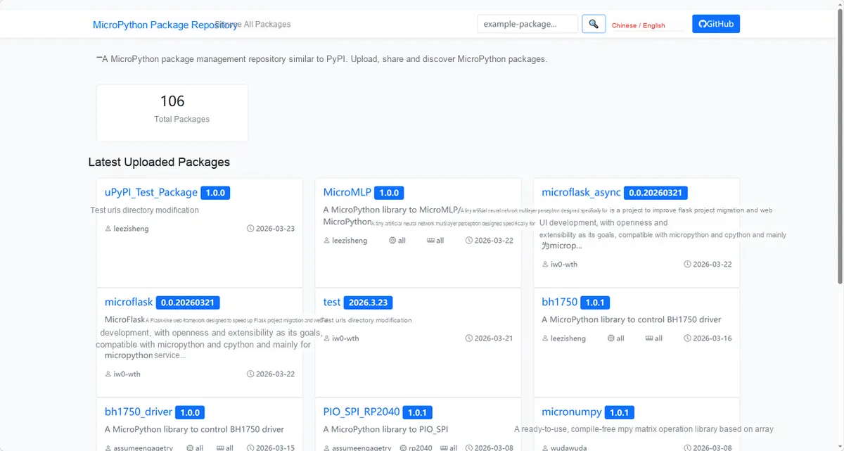
Here, we need to search for the relevant driver packages on uPyPI: https://upypi.net/zh/
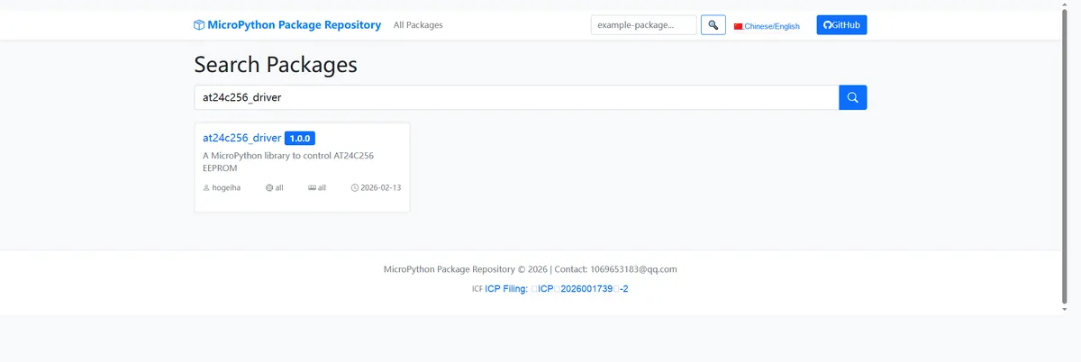
Enter at24c256_driver to search, and the following will be displayed:
Click to copy the local installation command:
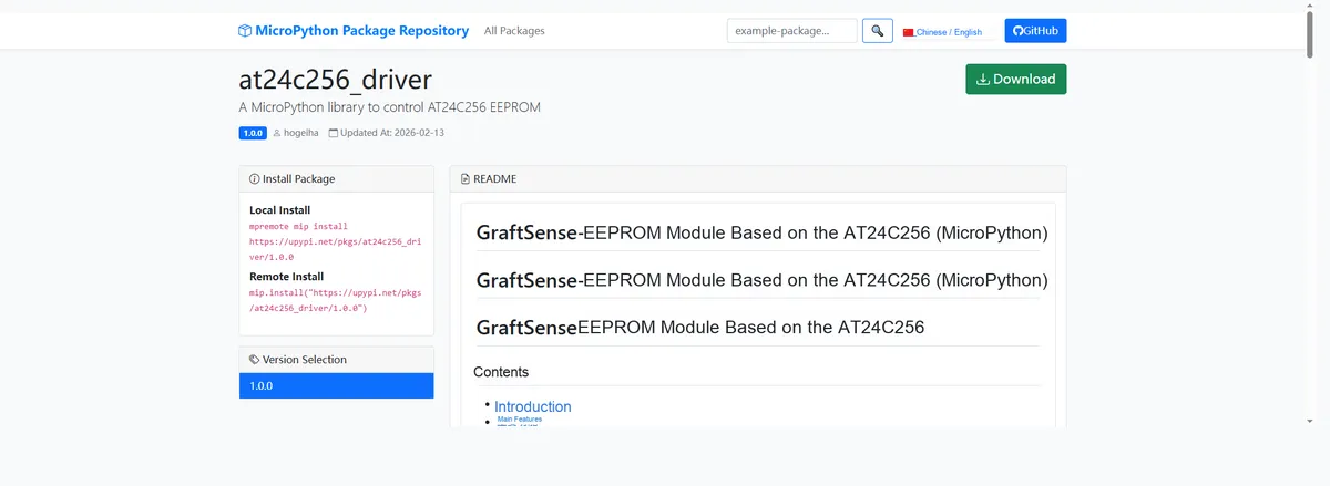
Here, we can import the module driver library code via the mip tool. Below are the usage commands for the mpremote tool:
mpremote mip install github:FreakStudioCN/GraftSense-Drivers-MicroPython/storage/at24c256_driverImport the EEPROM module based on AT24C256C - MicroPython driver code, then copy the following main.py code into our project:
# Python env   : MicroPython v1.23.0
# -*- coding: utf-8 -*-
# @Time    : 2024/9/27 10:44 AM
# @Author  : Li Qingshui
# @File    : main.py
# @Description : I2C experiment: read and write the external EEPROM chip AT24C256

# ======================================== Import Modules =========================================

# Hardware-related modules
from machine import I2C, Pin
from at24c256 import AT24CXX
# Time-related modules
import time

# ======================================== Global Variables ============================================

# The upper 7 bits are the address bits and the lowest bit is the read/write control bit: 0 for write, 1 for read
AT24C256_ADDRESS = 0xA0

# Define the number of bytes to write
DATA_SIZE = 128
# Generate a byte sequence from 0 to 127
data_to_write = bytes(range(DATA_SIZE))

# ======================================== Functions ============================================

def erase_data(at24cxx, start_address, length):
    '''
    Erase the specified area by filling it with 0xFF
    :param at24cxx   [AT24CXX]: AT24CXX class instance
    :param start_address [int]: Start address
    :param length        [int]: Write length
    :return: None
    '''

    # Generate byte data of length `length`, with all bytes set to 0xFF
    data_to_erase = bytes([0xFF] * length)
    # Write it continuously to the specified region
    at24cxx.write_page(start_address, data_to_erase)

# ======================================== Initialization ==========================================

# Power-on delay of 3 s
#time.sleep(3)
# Print debug message
print("FreakStudio: Read and Write AT24C256")

# Create a hardware I2C instance using the I2C1 peripheral, clock frequency 400KHz, SDA pin 10, SCL pin 11
i2c_at24c256 = I2C(id=0, sda=Pin(4), scl=Pin(5), freq=100000)

# Create an AT24C256 instance
at24c256 = AT24CXX(i2c_at24c256, AT24CXX.AT24C256, AT24C256_ADDRESS)

# ========================================  Main Program  ===========================================

# Verify whether the single byte and the 128 bytes read have been retained after power-off
if at24c256.read_byte(0) == 0xAB and list(at24c256.read_sequence(1, DATA_SIZE)) == list(data_to_write):
    print("Data verification successful. Data retained after power cycle.")
    # Erase the data of the first three pages
    erase_data(at24c256, 0, DATA_SIZE + 1)
# Determine this is the first write experiment
else:
    # Erase the data of the first three pages
    print("Erase the data of the first three pages")
    erase_data(at24c256, 0, DATA_SIZE + 1)

    # Write a single byte: write 0xAB to address 0x00
    print("Writing single byte...")
    at24c256.write_byte(0x00, 0xAB)
    print("Written single byte 0xAB at address 0x00.")

    # Read a single byte: read the data at address 0x00
    print("Reading single byte...")
    single_byte = at24c256.read_byte(0x00)
    print(f"Read single byte: {single_byte:#04x}")

    # Write 128 bytes to address 0x01
    print("Writing 128 bytes...")
    at24c256.write_page(0x01, data_to_write)
    print("Written 128 bytes starting at address 0x01.")

    # Read 128 bytes, starting at address 0x01
    print("Reading 128 bytes...")
    read_data = at24c256.read_sequence(0x01, DATA_SIZE)
    print(f"Read 128 bytes: {list(read_data)}")
Burn the code, open a terminal, and use the mpremote tool to connect to the main controller; the output is as follows:
In the main program, we performed the following operations:
- First, verify the power-off saving function: Check whether 0xAB has been written to address 0x00, and read the next 128 bytes of data to verify if it matches the generated byte sequence from 0 to 127. If the verification succeeds, print a success message and erase the data of the first three pages; if it fails, perform the initial write experiment.
- In the initial write experiment: erase the data of the first three pages, then write the single byte 0xAB to address 0x00, read this byte and print it, finally write 128 bytes starting with 0x01 as the first byte, and sequentially read 128 bytes from address 0x01 and print the results
Burn the program, open the terminal, and the following content will be displayed:
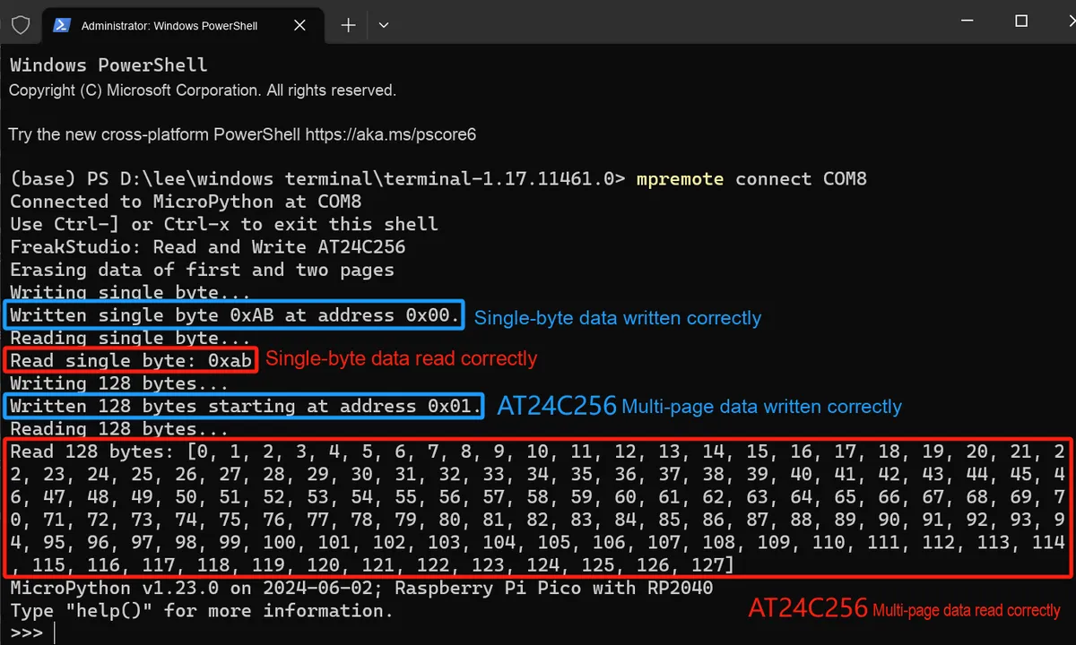
It can be seen that the customized AT24CXX class can implement the read and write functions for both bytes and pages. Next, we unplug the data cable connected to the Raspberry Pi Pico to simulate a power-off scenario, then reconnect it, open the terminal to connect to the Raspberry Pi Pico, and the display is as follows:
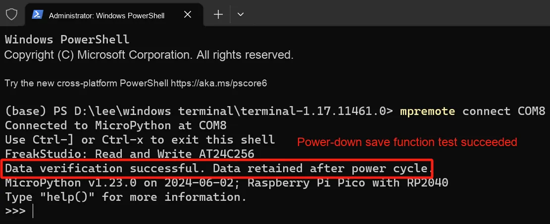
It can be seen that the data is still stored in the AT24C256 chip after power-off.
IV. Drivers
at24c256_driver.zip 6 KB
5. BOM & Recommended Alternative Parts
None.
VI. Revision History
Document Version | Date of Revision | Modifier | Modified Content |
v1.0 | 2025-11-23 | Li Zisheng | Initialize the document The BOM sheet has not been finally checked, the driver has not been re-verified, and the 3.3 application experiment Not yet specified. |
v1.1 | 2025-12-29 | Li Zisheng | Added application experiments and production files |
v1.2 | 2025-12-31 | Xin Ruili | Create an open version of the document based on the internal document version v1.1. |
v1.3 | 2026-03-29 | Xin Ruili | Modified the application experiment section |
VII. Relevant Materials
7.1 Chip Datasheet
C6482_EEPROM_AT24C256C-SSHL-T_Datasheet_MICROCHIP(Microchip_USA)_EEPROM_Datasheet.PDF 901 KB
7.2 Unique Icons for PCB Silkscreen