Contents
- I. Module Introduction
- II. Introduction to Major Chips
- 2.1 Chip Overview
- 2.2 Pin Definition
- 2.3 Functional Block Diagram
- 2.4 Performance Parameters
- 2.5 Reference Circuit
- 2.6 Chip Configuration
- 2.7 Communication Interfaces and Related Protocols
- 2.8 PCB Routing Precautions
- III. Circuit Engineering
- 3.1 Circuit Source Engineering
- 3.2 Module Usage Instructions
- 3.3 Application Experiment
- 4. Drivers
- 5. BOM & Recommended Alternative Parts
- VI. Revision History
- VII. Relevant Materials
- 7.1 Chip Datasheet
- 7.2 Unique Icons for PCB Silk Screen
I. Module Introduction
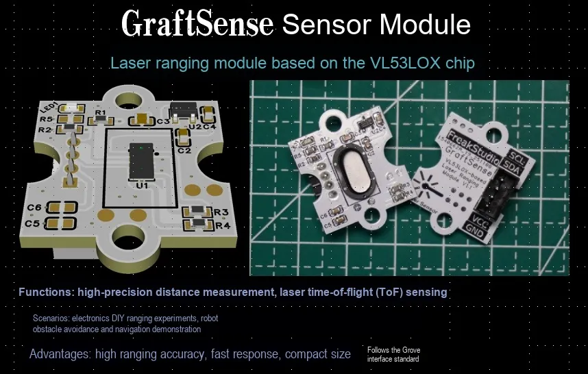
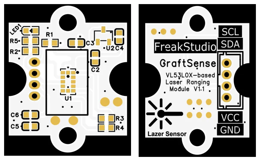
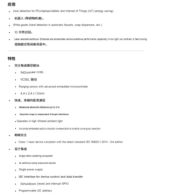
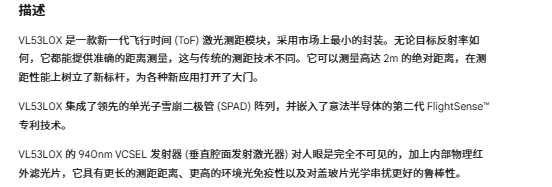
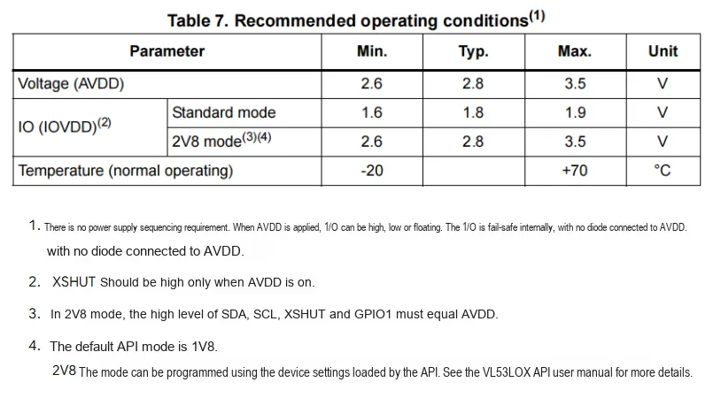
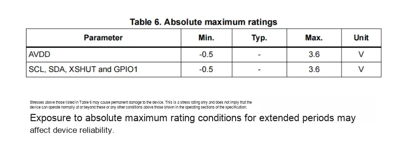
Laser ranging module based on VL53L0X chip is a ranging component that adopts ToF technology. The sensor operates at a voltage of 2.6V - 3.6V, the module's communication level is 3.3V, and it is equipped with MCU interface, power filtering and indicator light.It features a ranging range of 0-200cm (officially rated at 2m, with an effective optimized range of approximately 1.6m), an absolute accuracy within ±3%, immunity to target color, material or reflectance, a maximum refresh rate of 10Hz (default around 7Hz), operating current of ≈13mA in continuous mode, 40mA peak, and <5μA in standby, with a light source of Class 1 laser (compliant with the IEC 60825-1:2014 eye safety standard), and is suitable for scenarios requiring non-contact precise ranging such as drone obstacle avoidance, intelligent warehousing, and industrial ranging.
II. Introduction to Major Chips
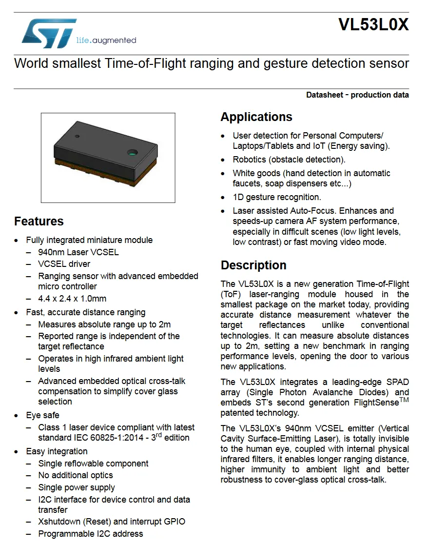
VL53L0X is a compact Time-of-Flight (ToF) laser ranging sensor launched by STMicroelectronics. It adopts 940nm infrared laser, with a typical ranging range from 0.5m to 2m, a precision of up to ±3%, and a fast ranging speed (the fastest is 30ms). It supports I²C interface, operates on 3.3V power supply with low power consumption (about 19mA in ranging mode and only 5μA in standby). Built with an optical system and signal processing circuit, it can effectively suppress ambient light interference, making it suitable for integration into scenarios that require short-range precise ranging such as mobile devices, robots, and security systems.
2.1 Chip Overview
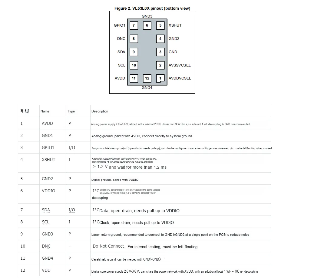
2.2 Pin Definition
2.3 Functional Block Diagram
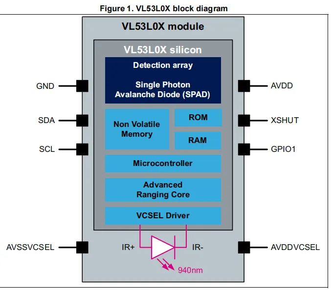
The following is VL53L0X the function description:
- Detection array (Single Photon Avalanche Diode,
SPAD)- The single-photon avalanche diode array is responsible for receiving 940nm infrared laser photons reflected by the target, converting optical signals into electrical signals, realizing photon-level signal detection, and providing original signal input for ranging.
- Non Volatile Memory, ROM, RAM
- Non-volatile memory is used to store persistent data such as chip configuration parameters; ROM stores chip firmware and basic programs; and RAM is used for temporary data storage and operations during runtime, ensuring the storage and invocation of chip programs and data.
- Microcontroller
- As the control core of the chip, it coordinates the operations of various modules, processes instructions from the external main controller, and manages data read-write and arithmetic processes, serving as the "command center" of the chip.
- Advanced Ranging Core
- The advanced ranging core unit, based on the signals received by
SPAD, calculates the time elapsed from laser emission to reception using the time-of-flight (ToF) algorithm, and then converts it into the target distance, which is a key module for achieving precise ranging.
- The advanced ranging core unit, based on the signals received by
- VCSEL Driver
- A vertical-cavity surface-emitting laser (
VCSEL) driver module, which generates a driving signal to enable theIR+andIR-pins-connectedVCSELto emit 940nm infrared laser, providing an emission light source for ranging.
- A vertical-cavity surface-emitting laser (
- Control and Communication Interfaces (
SDA,SCL,XSHUT,GPIO1)SDA,SCL: Compatible with I²C communication timing, enabling instruction interaction between the chip and the external main control as well as ranging data postback.XSHUT: Shutdown control pin, which can be used to enable or disable the operation of the chip.GPIO1: A general-purpose input/output pin that can be used for functions such as interrupt feedback.
- Power supply module (
GND,AVDD, AVSSVCSEL, AVDDVCSEL)- Multiple sets of power supply pins are provided to supply power to partitions such as the analog circuit (AVDD) and the VCSEL driver circuit (AVDDVCSEL), with GND and AVSSVCSEL serving as ground terminals to ensure stable power supply for each module of the chip.
Typical Scenarios (Taking Ranging as an Example):
- Transmission: The main controller sends commands via the I²C interface → the microcontroller controls the VCSEL driver → which drives the VCSEL to emit 940nm infrared laser.
- Reception and Processing: The laser reflected by the target is received by the SPAD array and converted into an electrical signal → the signal is sent to the Advanced Ranging Core, where the distance is calculated in combination with the ToF algorithm → the ranging data is postback to the main controller via the I²C interface.
2.4 Performance Parameters
2.5 Reference Circuit
2.6 Chip Configuration
VL53L0X requires no additional configuration during use.
2.7 Communication Interfaces and Related Protocols
2.7.1 Control Interface Description
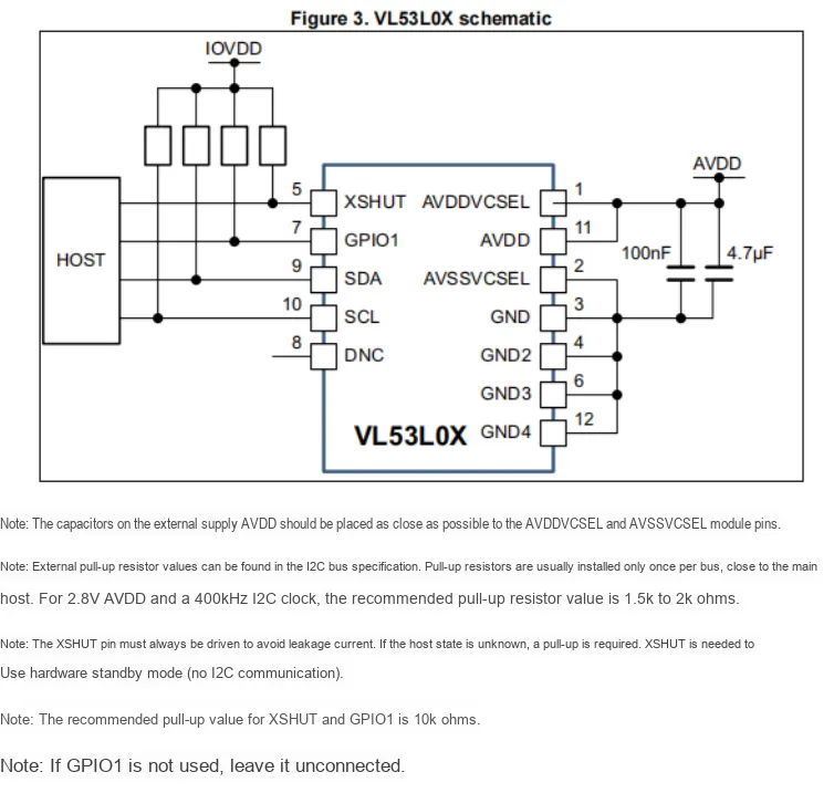
The I²C interface uses two signals: the Serial Data Line (SDA) and the Serial Clock Line (SCL). Every device connected to the bus is assigned a unique address, and a simple master/slave relationship applies to the bus structure.
Both the SDA and SCL lines are connected to the positive supply voltage via pull-up resistors located on the host. The lines are only actively pulled low. When a line is in a floating state and the pull-up resistor pulls the line high, this corresponds to a high logic level. When no data is being transmitted, both lines are held at a high level.
The clock signal (SCL) is generated by the master device, which initiates data transmission. On the VL53L0X, the maximum speed of the I²C bus is 400 kbits/s, and the device address is 0x52.
Data Transmission Protocol
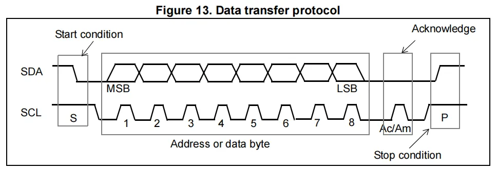
Information is packaged in the form of 8-bit data packets (bytes), and each byte is always followed by an acknowledge bit. Internal data is generated by sampling SDA on the rising edge of SCL. External data must remain stable while SCL is at a high level. The exceptions are the start (S) or stop (P) conditions, in which SDA falls or rises respectively when SCL is at a high level.
A message consists of a sequence of bytes starting with a start condition, followed by either a stop condition or a repeated start (another start condition without a preceding stop condition). The first byte contains the device address (0x52) and also specifies the data direction. If the least significant bit is low (i. e., 0x52), the message is a master writing data to a slave; if the least significant bit is high (i. e., 0x53), the message is a master reading data from a slave.
Figure 14. VL53L0X I²C Device Address: 0x52 (Bit Structure: From Most Significant Bit (MSBit) to Least Significant Bit (LSBit), the bits are 0,1, 0,1, 0,0, 1, R/W in sequence)

All serial interface communications of the module must start with a start condition. The VL53L0X module acknowledges the reception of a valid address by pulling SDA low. The state of the read/write bit (lsb of the address byte) of the address byte is stored, and the data of the next byte is sampled via SDA. In a write sequence, the second byte received provides an 8-bit index pointing to one of the internal 8-bit registers.
2.7.2 L53L0X Data Format (Write Operation)
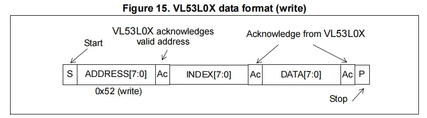
When receiving data from a slave device, the data is written bit by bit into the serial/parallel register. After receiving each data byte, the slave device generates an acknowledge signal, and then the data is stored in the internal register addressed by the current index.
During message reading, the content of the register addressed by the current index is read out in the byte following the device address byte. The content of this register is parallel-loaded into the serial/parallel register and is latched out from the device on the falling edge of SCL.
2.7.3 VL53L0X Data Format (Read Operation)
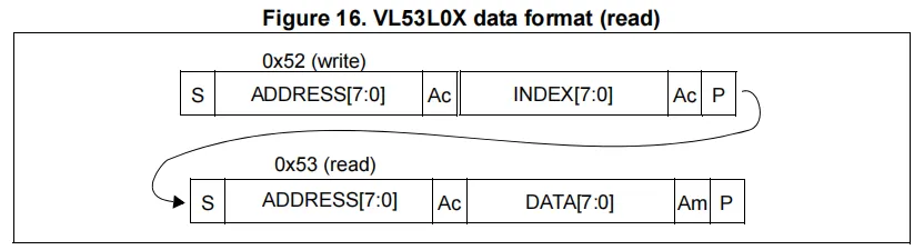
In the read-write message sequence, at the end of each byte, the receiving device will send an acknowledgment (for write operations, it is the VL53L0X that sends the acknowledgment; for read operations, it is the host that sends the acknowledgment).
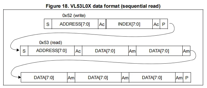
A message can only be terminated by the bus master, either by issuing a stop condition, or by sending a negative acknowledge (i. e., not pulling the SDA line low) after reading a complete byte.
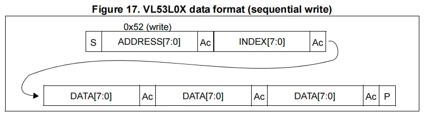
This interface also supports an auto-increment index function. After the first data byte is transmitted, the index is automatically incremented by 1. Therefore, the master device can continuously send data bytes to the slave device until the slave device fails to provide an acknowledgment or the master device terminates the write communication with a stop condition. If the auto-increment function is used, the master device does not need to send an address index to accompany the data bytes.
2.7.4 VL53L0X Data Format (Continuous Write Operation)
2.7.5 VL53L0X Data Format (Continuous Read Operation)
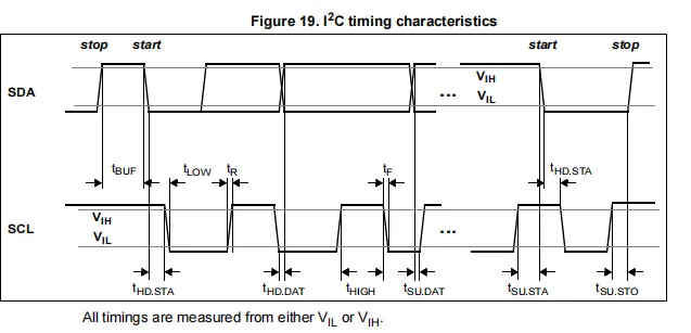
2.7.6 I2C Interface - Timing Characteristics
The timing characteristics are shown in the figure above. For the description of the parameters used, please refer to the following table.
Timing is applicable to all PVT (Process, Voltage, Temperature) conditions.
Table 3. I²C Interface - Timing Characteristics
| Symbol | Parameter | Min | Typ | Max | Unit |
| FI2C | Operating frequency (standard mode and fast mode) | 0 | - | 400 | kHz |
| tLOW | Clock low pulse width | 1.3 | - | - | μs |
| tHIGH | Clock high pulse width | 0.6 | - | - | μs |
| tSP | Spike pulse width suppressed by the input filter | - | - | 50 | ns |
| tBUF | Bus free time between transmissions | 1.3 | - | - | ms |
| tHD.STA | Start hold time | 0.26 | - | - | μs |
| tSU.STA | Start setup time | 0.26 | - | - | μs |
| tHD.DAT | Data hold time | 0 | - | 0.9 | μs |
| tSU.DAT | Data setup time | 50 | - | - | ns |
| tR | SCL/SDA rise time | - | - | 120 | ns |
| tF | SCL/SDA fall time | - | - | 120 | ns |
| tSU.SRO | Stop setup time | 0.6 | - | 10 | μs |
| CIO | Input / output capacitance (SDA) | - | - | 10 | pF |
| CIin | Input capacitance (SCL) | - | - | 4 | pF |
| CL | Load capacitance | - | 125 | 400 | pF |
- The maximum bus speed is also limited by the combination of a 400 pF load capacitance and pull-up resistors. For further information, refer to the I²C specification.
2.7.7 I²C Timing Characteristics
2.7.8 I²C Interface - Reference Registers
The registers shown in the following table can be used to verify the user's I²C interface.
Table 4. Reference Registers
| Address | (Value after a brand-new reset with no API loaded) |
| 0xC0 | 0xEE |
| 0xC1 | 0xAA |
| 0xC2 | 0x10 |
| 0x51 | 0x0099 |
| 0x61 | 0x0000 |
Note: I²C read and write operations can be 8-bit, 16-bit or 32-bit. Multi-byte read and write operations always address in ascending order, with the most significant bit (MSB) first, as shown in Table 5.
Table 5. Example of 32-bit Register
| Register address | Byte |
| Address | MSB |
| Address + 1 | ... |
| Address + 2 | ... |
| Address + 3 | LSB |
2.8 PCB Routing Precautions
None.
III. Circuit Engineering
3.1 Circuit Source Engineering
To obtain the circuit source project, please follow the official account [Freak Embedded]
3.2 Module Usage Instructions
SCH_Schematic1_VL53L0X-Based Laser Ranging Module_v1.0_2025-11-11.pdf 2.2 MB
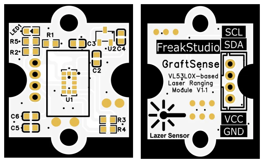
This module provides a I2C digital communication interface: it supports standard I2C communication rates, with a default I2C address of 0x29 (configurable on demand), is compatible with 3.3V logic levels, and can stably transmit accurate ranging data within the range of 0-200cm (with an absolute accuracy within ±3%, unaffected by the target's color or material). Its maximum refresh rate reaches 10Hz, making it suitable for scenarios such as UAV obstacle avoidance, intelligent warehousing ranging, and distance detection for maker projects, and provides reliable digital data interaction capabilities for non-contact accurate ranging applications.
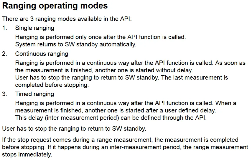
When using this module, it is necessary to pay attention to the differences between its different operating modes:
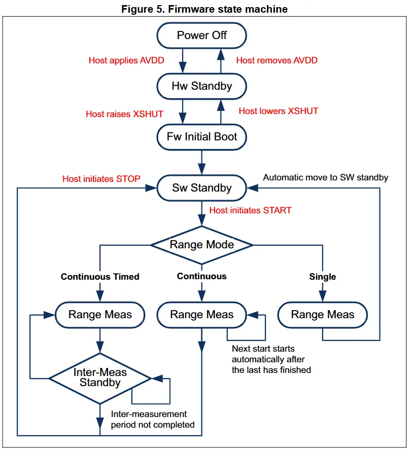
First, the module must complete the boot sequence from " Power Off → Hw Standby → Fw Initial Boot ", and after entering the " Sw Standby " state, it can accept a Host -initiated START command to enter the ranging mode (Range Mode). The core usage differences among the three modes are as follows:
- Single ranging mode (
Single ranging): After triggeringSTART, only one ranging operation will be performed. Once completed, the module will automatically return to theSw Standbystate without manual stop operation.- Note: It is suitable for single-distance detection scenarios (e. g., point measurement requirements of "one trigger, one measurement"), and no additional stop operation is required.
- Continuous ranging mode (
Continuous ranging): After triggeringSTART, the device will continuously perform ranging in cycles, starting the next measurement immediately without delay once the previous one is completed; it will only stop when theHostactively issues aSTOPcommand, and will return toSw Standbyafter the ongoing measurement is finished.- Note: It is suitable for real-time continuous ranging scenarios (such as dynamic Object Tracking), but remember to stop it actively to prevent the module from running continuously.
- Timed continuous ranging mode (
Timed ranging): After triggeringSTART, continuous ranging is performed in the same way, but a user-defined interval is inserted between two measurements; there are two stop logics: if theSTOPcommand is issued during a measurement, the system will stop after the current measurement is completed; if it is issued during the interval, the system will stop immediately and return toSw Standby.- Note: This is suitable for periodic sampling scenarios (e. g., fixed-interval environmental distance monitoring), and the interval duration needs to be set in advance via
API.
- Note: This is suitable for periodic sampling scenarios (e. g., fixed-interval environmental distance monitoring), and the interval duration needs to be set in advance via
3.3 Application Experiment
Here, we use the GraftPort-RP2040 development board for testing, and the laser ranging module based on the VL53L0X chip uses the I2C interface to communicate with the main controller.
Here, we first use the HY2.0-4P cable to connect the module to the GraftPort-RP2040 development board's I2C0 interface:
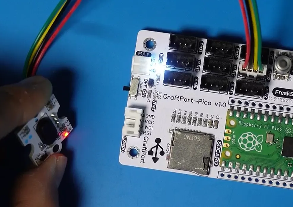
The module connections are shown in the following table:
Development Board Pins | Module Pins | Description |
Pin 4 |
|
|
Pin 5 |
|
|
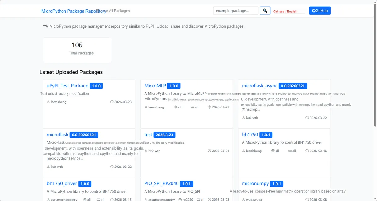
Here, we need to search for the relevant driver packages on uPyPI: https://upypi.net/zh/
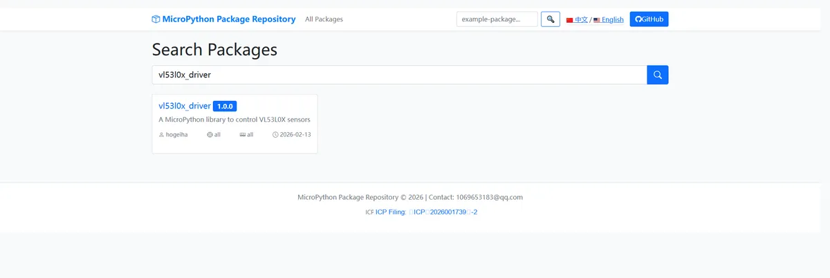
Enter vl53l0x_driver to search, and the following will be displayed:
Click to copy the local installation command:
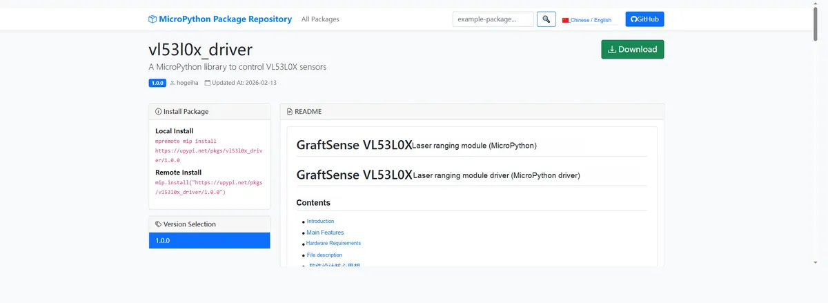
Here, we can import the module driver library code via the mip tool. Below are the usage commands for the mpremote tool:
mpremote mip install github:FreakStudioCN/GraftSense-Drivers-MicroPython/sensors/vl53l0x_driverImport the MicroPython driver code for the VL53L0X chip-based laser ranging module, then copy the following main.py code into our project:
# Python env   : MicroPython v1.23.0
# -*- coding: utf-8 -*-
# @Time    : 2025/9/5 10:39 AM
# @Author  : 缪贵成
# @File    : main.py
# @Description : Test file for the vl53l0x-based laser distance sensor module driver

# ======================================== Import Modules =========================================

import time
import machine
from vl53l0x import VL53L0X

# ======================================== Global Variables ============================================

vl530_addr = None

# ======================================== Functions ============================================

# ======================================== Custom Classes ============================================

# ======================================== Initialization configuration ===========================================

#time.sleep(3)
print("FreakStudio: Testing VL53L0X Time-of-Flight sensor")

# Initialize I2C (Raspberry Pi Pico uses I2C0, default pins GP4=SDA, GP5=SCL)
i2c = machine.I2C(0, scl=5, sda=4, freq=100000)
# Start scanning for devices on the I2C bus and return a list of slave addresses
devices_list:list[int] = i2c.scan()
print('START I2C SCANNER')
# If the devices list is empty, no device is connected to the I2C bus
if len(devices_list) == 0:
    # If not empty, print the slave device addresses
    print("No i2c device !")
else:
    print('i2c devices found:', len(devices_list))
for device in devices_list:
    if 0x20 <= device <= 0x50:
        print("I2c hexadecimal address:", hex(device))
        vl530_addr = device

# Initialize the VL53L0X sensor
tof = VL53L0X(i2c, vl530_addr)
print("VL53L0X initialized successfully")

# ======================================== Main Program ==============================================
try:
    # Set to continuous measurement mode, 50ms period
    tof.start()
    while True:
        # Read the distance, in mm
        distance = tof.read()
        if distance > 0 and distance < 2000:
            print("Distance: %d mm" % distance)
        else:
            print("Out of range or read error")
        time.sleep(0.8)

except KeyboardInterrupt:
    print("\nProgram terminated by user")
finally:
    # Stop measurement
    tof.stop()
    print("Testing completed")
Burn the code, open the terminal, and use the mpremote tool to connect to the main controller. The output is as follows:
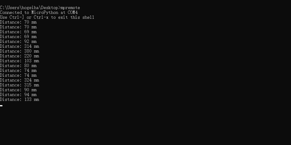
It can be seen that when our palm moves continuously in front of the sensor, the terminal will print out the measured values:
4. Drivers
vl53l0x_driver.zip 18 KB
5. BOM & Recommended Alternative Parts
None.
VI. Revision History
Document Version | Date of Modification | Modifier | Revised Content |
v1.0 | 2025-11-11 | Zero Kōkō | Initialize Document |
v1.1 | 2025-12-29 | Li Zisheng | Added application experiments and production files |
v1.2 | 2025-12-31 | Xin Ruili | Create an open version of the document based on the internal document version v1.1. |
v1.3 | 2026-03-29 | Xin Ruili | Modified the application experiment section |
VII. Relevant Materials
7.1 Chip Datasheet
VL53L0X.pdf 918 KB
7.2 Unique Icons for PCB Silk Screen