Contents
- I. Module Introduction
- II. Introduction to Main Chips
- 2.1 Chip Overview
- 2.2 Pin Definition
- 2.3 Functional Block Diagram
- 2.4 Performance Parameters
- 2.5 Reference Circuit
- 2.6 Chip Configuration
- 2.7 Communication Interfaces and Related Protocols
- 2.8 PCB Routing Precautions
- III. Circuit Engineering
- 3.1 Circuit Source Engineering
- 3.2 Module Usage Instructions
- 3.3 Application Experiment
- IV. Drivers
- 5. BOM & Recommended Alternative Parts
- VI. Revision History
- 7. Relevant Materials
- 7.1 Chip Datasheet
- 7.2 Unique Icons for PCB Silk Screen
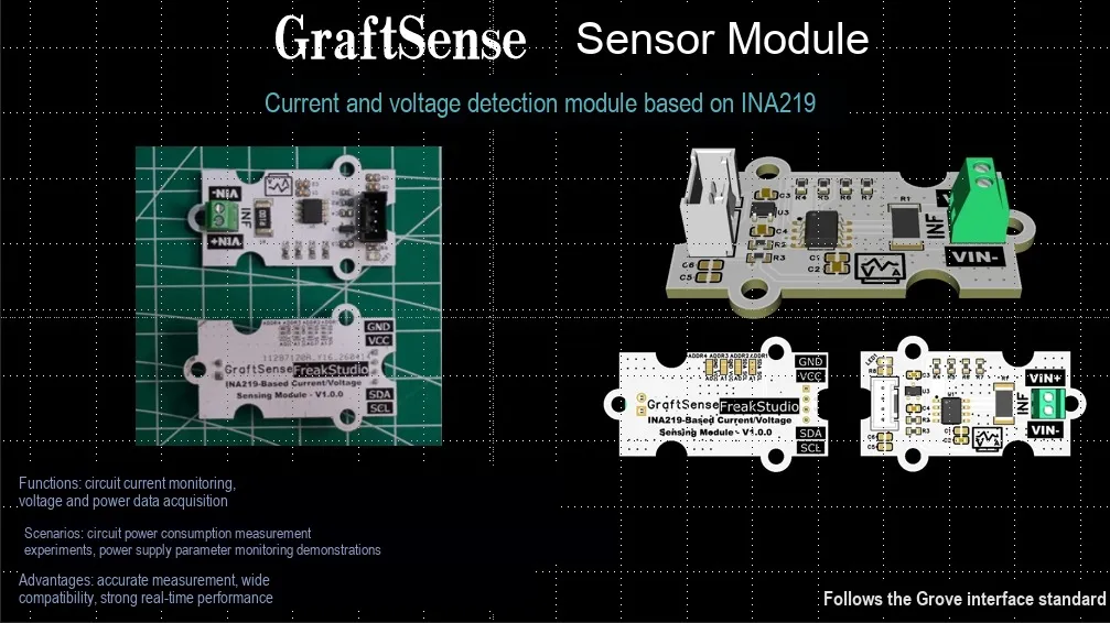
I. Module Introduction
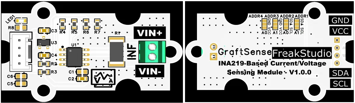
Current and Voltage Detection Module Based on INA219, which adopts the INA219 chip solution, realizes bidirectional current, voltage and power monitoring via the I2C interface. Built with a 16-bit ADC, it can measure ±3.2A current and 0~26V bus voltage with a matched sampling resistor; the module is equipped with an address selection circuit, an LDO voltage regulator circuit, power filtering and indicator circuit, powered by 3.3V with an operating voltage range of 3.0~5.5V. Featuring high precision and low power consumption, it is applicable to scenarios such as battery management, power supply monitoring, and energy consumption monitoring of DC systems.
II. Introduction to Main Chips
INA219 is a TI -manufactured, I²C -interfaced zero-drift bidirectional current/voltage/power monitoring chip that supports bus voltage measurement from 0 to 26V and allows direct reading of current and power values.
2.1 Chip Overview
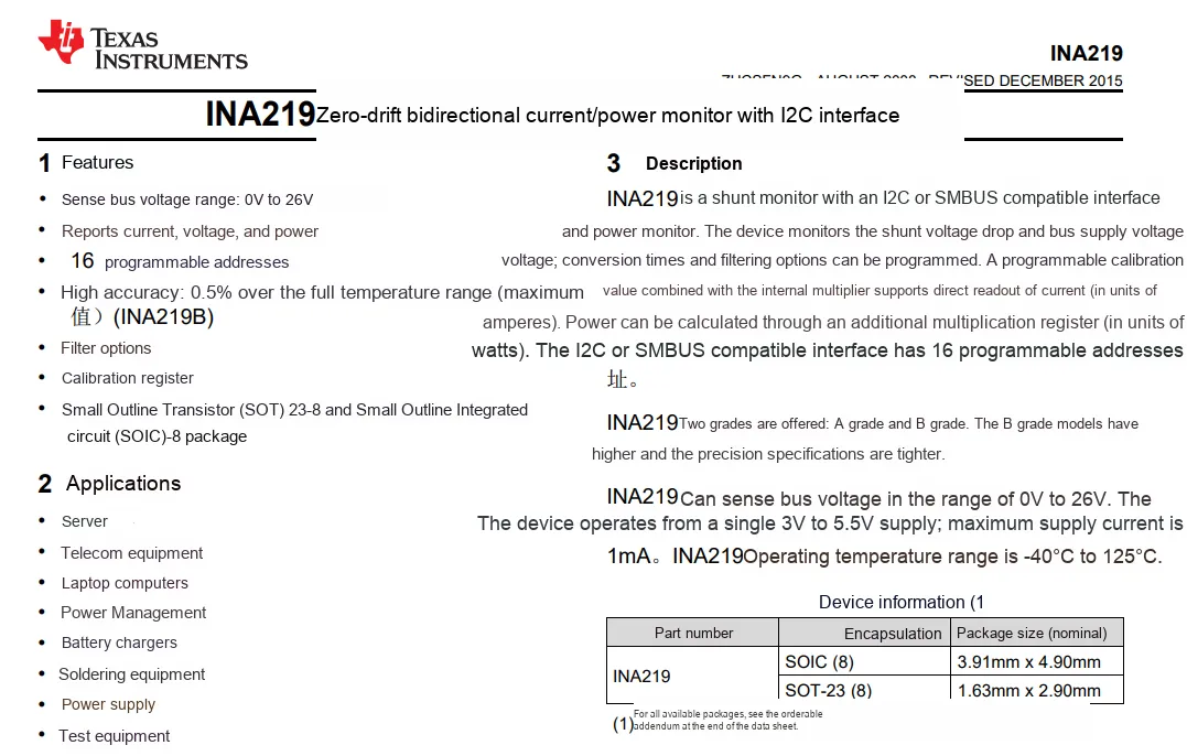
INA219 is a TI -launched I²C / SMBus interface zero-drift bidirectional current/power monitoring chip. It supports bus voltage measurement from 0 to 26V, can directly read current, voltage and power values, features 16 programmable addresses, filtering options and calibration registers, offers A/B grade accuracy (the maximum error of B grade is 0.5%), adopts SOIC-8 or SOT-23-8 packages, is suitable for scenarios such as servers and power management, operates at a temperature range of -40°C to 125°C, and has a supply voltage of 3V to 5.5V.
2.2 Pin Definition
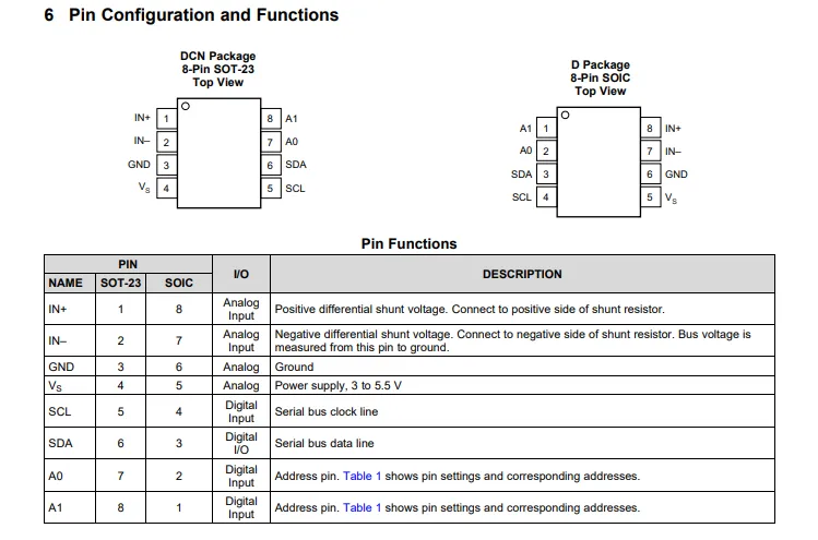
SOT-23 and SOIC-8 packages both feature differential sampling inputs (IN+ / IN-), power supply (Vs, 3-5.5V), ground (GND), an I²C interface (SCL / SDA), as well as I²C address pins A0 / A1 for configuring 16 addresses; the functions of each pin are clearly specified in the table.
2.3 Functional Block Diagram
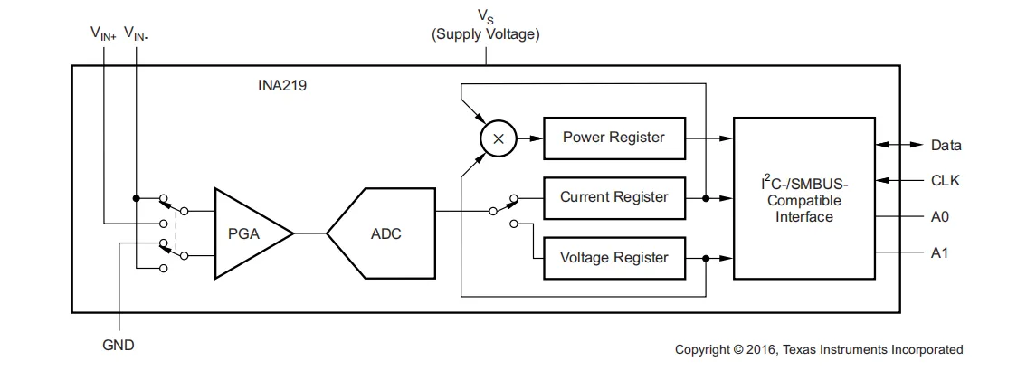
INA219 / IN+ / IN- pins, which are amplified by a programmable gain amplifier (PGA) and then sent to the ADC for conversion. The conversion results are stored in the current and voltage registers respectively, the power value is calculated by the multiplier and stored in the power register, and finally provided to the host for reading through the I²C / SMBus interface. The A0 / A1 pins are used to configure the device address to realize multi-device bus mounting.
2.4 Performance Parameters
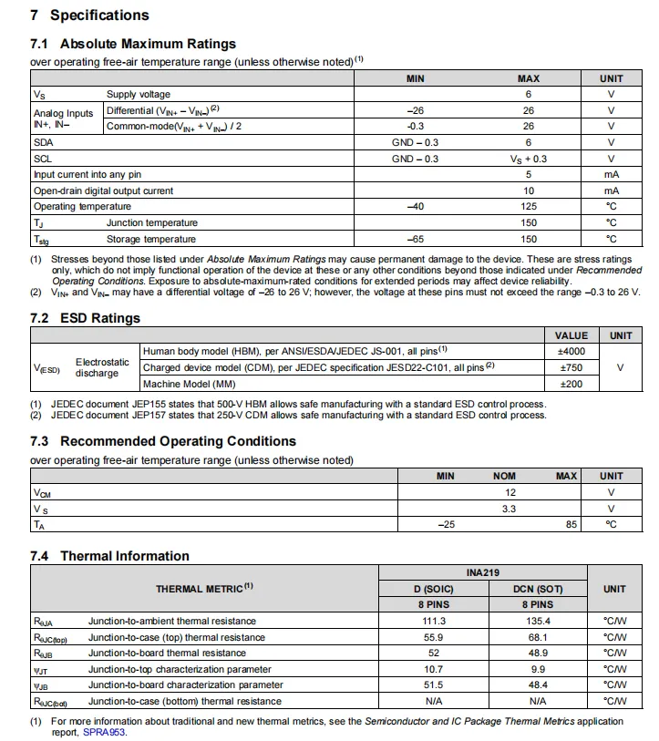
INA219 Key Absolute Maximum Ratings and Operating Conditions: The power supply voltage (Vₛ) has a maximum value of 6V, the differential voltage range of analog input is -26V to 26V, the common-mode voltage range is -0.3V to 26V, and the voltage of digital pins shall not exceed Vₛ + 0.3V; For ESD protection, the HBM mode is ±4000V, the CDM mode is ±750V, and the MM mode is ±200V;The recommended operating conditions are a power supply of 3.3V, a maximum common-mode voltage of 12V, and an operating temperature range of -25°C to 85°C; meanwhile, the thermal resistance parameters for the two packages SOIC and SOT are also provided.
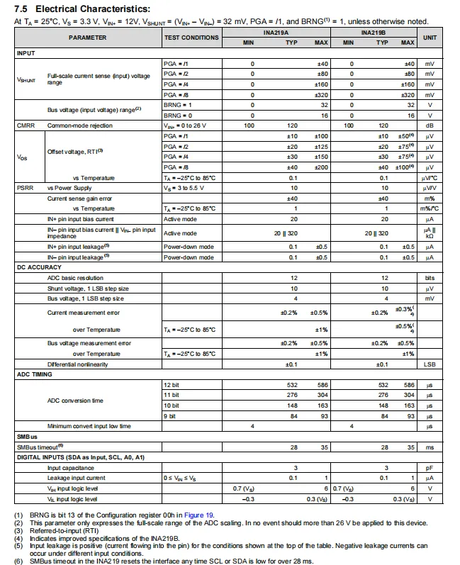
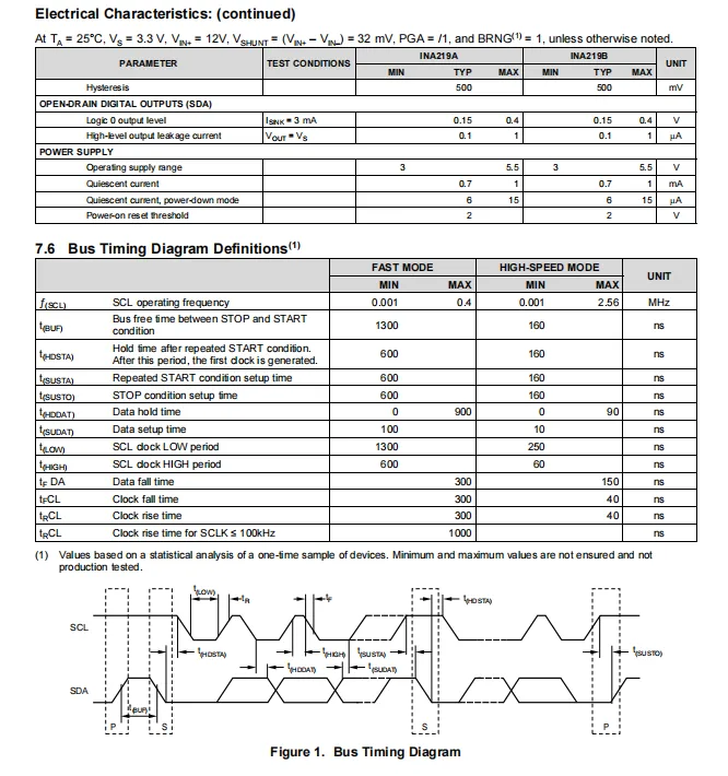
Under the supply conditions of 25℃ and 3.3V, its current sensing input voltage range is adjustable with the PGA gain, the maximum bus voltage measurement reaches 32V (when BRNG = 1), the typical current measurement error is ±0.2%(Class B performs better), and the ADC conversion time varies with the resolution; in terms of digital interfaces, the I²C fast mode supports up to 400kHz and the high-speed mode can reach 2.56MHz. Meanwhile, the timing parameters such as clock setup/hold time and rise/fall time, as well as key indicators including power supply, leakage current, output level and power consumption are also provided.
2.5 Reference Circuit
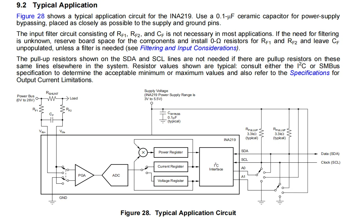
The power supply bus is connected to the load via a sampling resistor RSHUNT; the chip's VIN+ / VIN- pins are connected across the sampling resistor, with optional RF1 / RF2 / CF to form input filtering. A 0.1μF capacitor is used for decoupling at the power supply terminal; the I²C interface's SDA / SCL require 3.3kΩ pull-up resistors, and the A0 / A1 pins configure the I²C address by connecting to ground or power supply, finally realizing the monitoring and output of current, voltage and power.
2.6 Chip Configuration
None.
2.7 Communication Interfaces and Related Protocols
2.7.1 I2C Communication
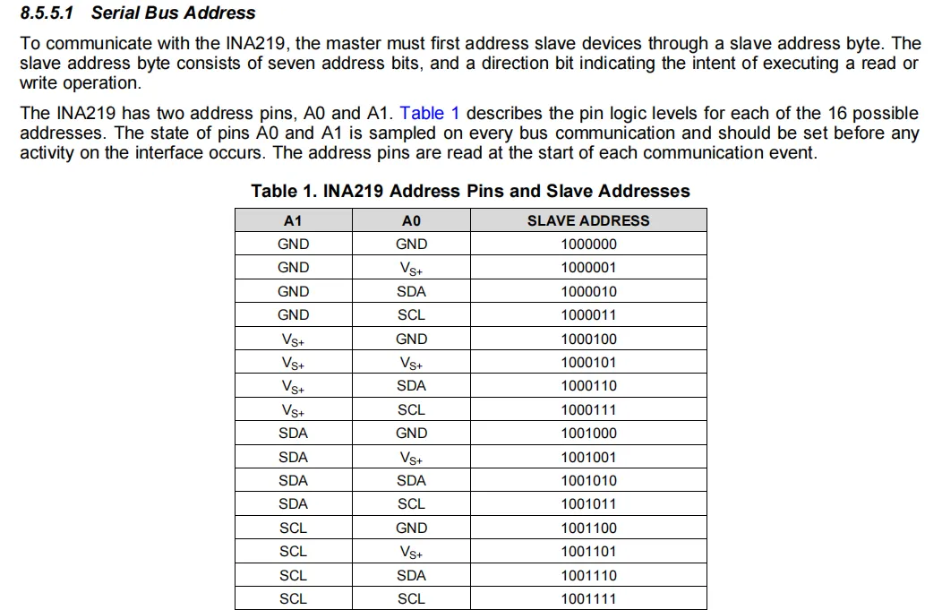
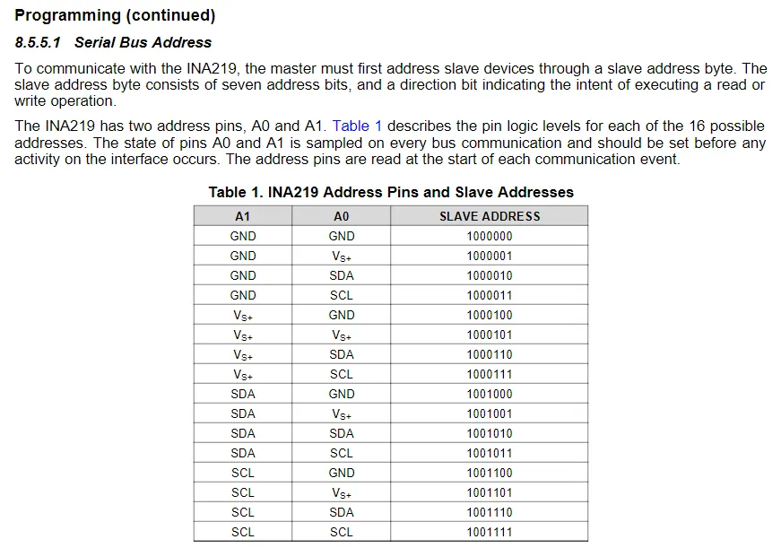
Through the two address pins A0 and A1, 16 different 7-bit slave addresses can be configured; the pin states can be connected to GND, Vs+, SDA or SCL, and the combination forms a unique address which is sampled and read at the start of each bus communication.
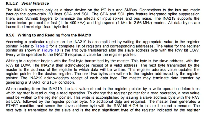
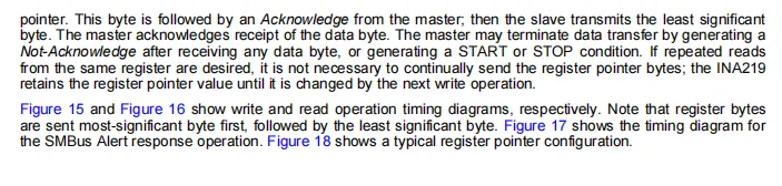
INA219 operates only as an I²C / SMBus slave. The SDA / SCL pins integrate spike suppression and Schmitt triggers, supporting Fast Mode (400kHz) and High-Speed Mode (2.56MHz), with data transmitted in MSB-first order.For read and write operations, the register pointer address must be sent first. During a write operation, the master sends the slave address (R/W = 0), the register address, and two data bytes. For a read operation, the register pointer must first be written, then a repeated start condition is used to switch to read mode (R/W = 1), after which the slave returns data with the higher-order bit first followed by the lower-order bit. The register pointer retains its current value and does not need to be reset for every read operation.
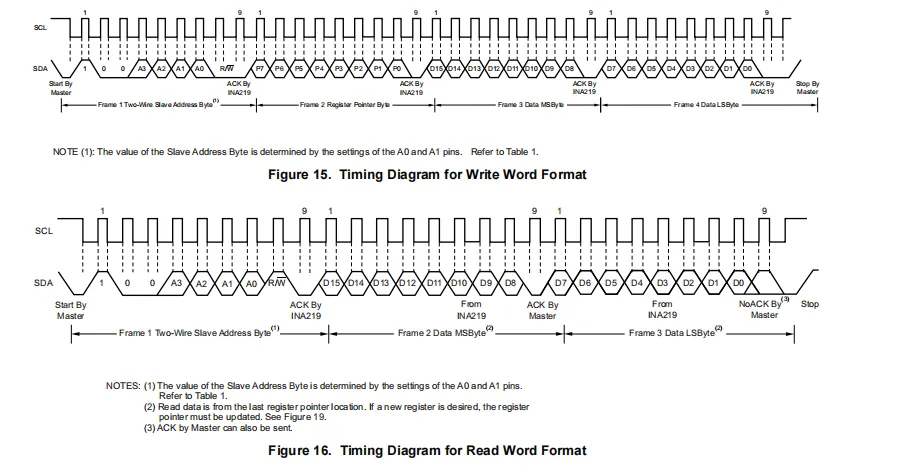
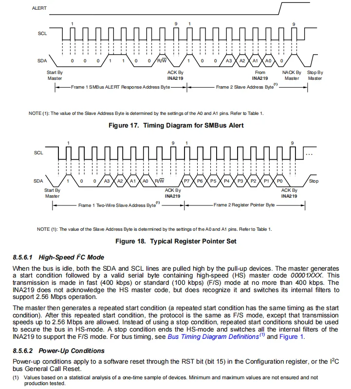
INA219 I²C communication process: During a write operation, the master sends the slave address (R/W = 0), register pointer, and two data bytes (most significant byte first), and the slave responds with ACK byte by byte; for a read operation, the register pointer must first be set via a write operation, then switch to read mode with a repeated start (R/W = 1), the slave returns data with the most significant byte first, and the master terminates communication by responding with NACK on the last byte. In addition, the SMBus Alert response timing and register pointer setting process are provided, and the switching method and power-on conditions for the high-speed I²C mode are described.
2.7.2 Registers
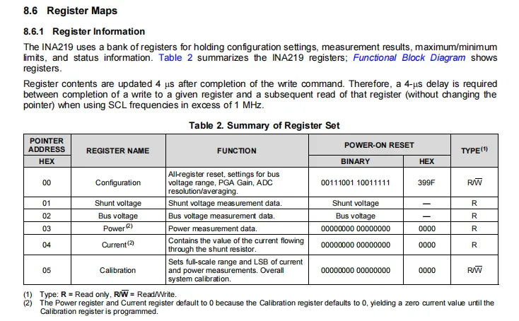
The register map of INA219 consists of 6 core 16-bit registers: the configuration register (address 00h, read/write, reset value 399Fh) is used to set measurement parameters; the shunt voltage (01h), bus voltage (02h), power (03h) and current (04h) registers are read-only registers for measurement results; the calibration register (05h, read/write, reset value 0000h) is used to configure the full-scale range and LSB value. The default values of the current and power registers are 0, and valid data can only be output after calibration.In addition, a 4μs update time is required after register writing, so attention should be paid to the delay during high-speed communication.
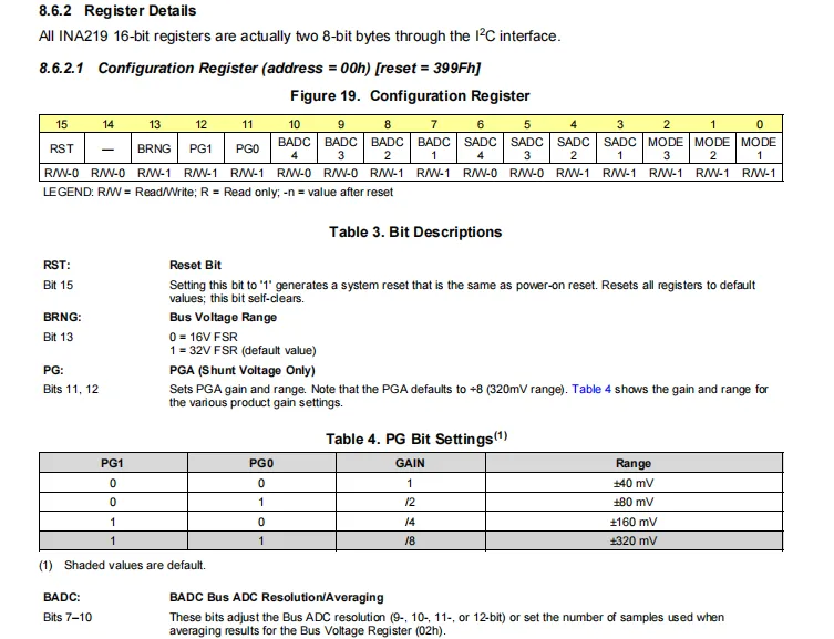
INA219 Configuration Register Details: This 16-bit register (address 00h, reset value 399Fh) contains control bits including RST, BRNG, PG, BADC, SADC, MODE, which enable system reset, bus voltage range selection (16V/32V), PGA gain setting for shunt voltage (1/2/4/8x, default 8x corresponding to ±320mV), bus/shunt ADC resolution and sampling averaging configuration, as well as operating mode setting. All configurations are read from and written to via the I²C interface in double-byte format.
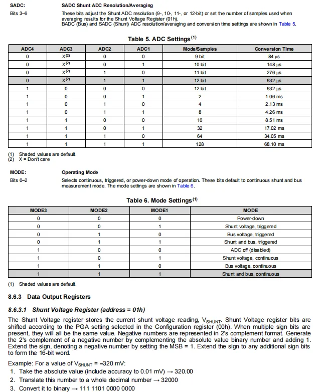
ADC resolution / average setting (SADC / BADC): 9-12 bit resolution or 2-128 sampling averages are configurable; the conversion time ranges from 84μs to 68.10ms depending on the configuration, with a default of 12-bit single sampling.
Operating Mode (MODE): Configurable via 3 bits to support power-down, single-shot trigger or continuous measurement; the default mode is continuous shunt and bus voltage measurement.
Shunt Voltage Register (01h): Stores the shunt voltage value in two's complement format. The data is shifted according to the PGA setting in the configuration register, and can represent both positive and negative voltages. An example is provided to illustrate the conversion method for -320mV.
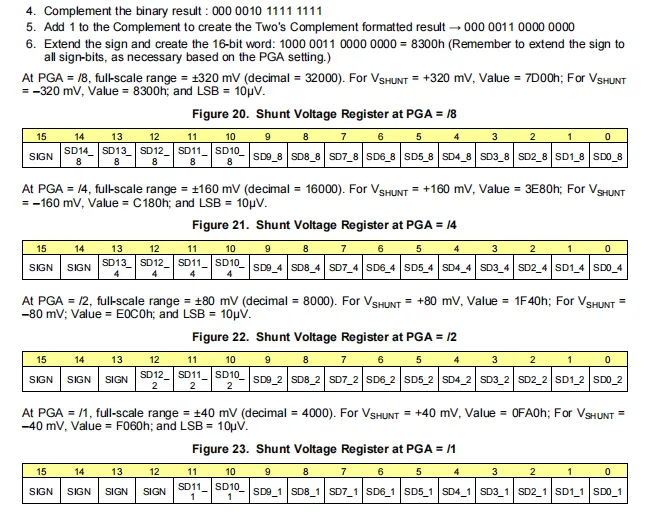
INA219 Storage Format and Calculation Method of Shunt Voltage Register Under Different PGA Gains: The register stores voltage values in two's complement, and the number of data bits varies with PGA (/8, /4, /2, /1); the highest bit is the sign bit, and some high bits need to be sign-extended according to the gain. Different gains correspond to different full-scale ranges (±320mV/±160mV/±80mV/±40mV), LSB is fixed at 10µV, and examples of register values corresponding to positive and negative full-scale voltages are also provided.
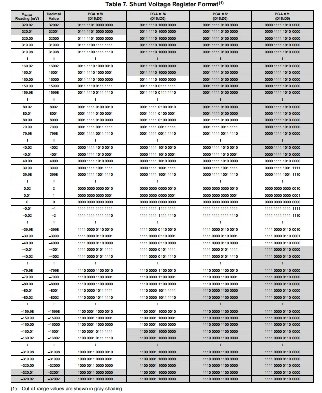
Bus Voltage Register (Address 02h): Stores the measured bus voltage value, with a full-scale range of 32V (LSB = 4mV) or 16V (LSB = 4mV), and the least significant two bits contain the conversion ready (CNVR) and overflow flag (OVF).
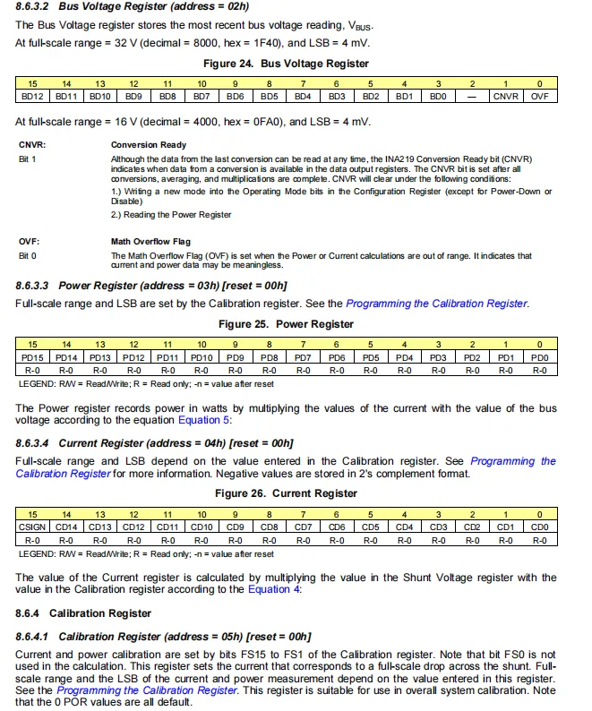
Power Register (Address: 03h, Reset Value: 00h): Stores the calculated power value; its full-scale range and LSB are configured via the calibration register, and this is a read-only register.
Current Register (Address 04h, Reset Value 00h): Stores the current value in two's complement format; its measurement range and LSB are also determined by the calibration register, and it is a read-only register.
Calibration Register (Address: 05h, Reset Value: 00h): Configures the measurement ranges for current and power as well as LSB by setting the current value corresponding to the full-scale shunt voltage to achieve system calibration.

Calibration Register (Address 05h): In the 16-bit structure, only FS15 to FS1 are read-write bits; the least significant bit FS0 is read-only and always fixed at 0, and the actual calibration value is stored in the upper 15 bits. This register is used to configure the full-scale range and LSB value for current and power measurement, which needs to be calculated and written according to the shunt resistance value and target current range, serving as a key configuration for accurate current and power measurement.
2.8 PCB Routing Precautions
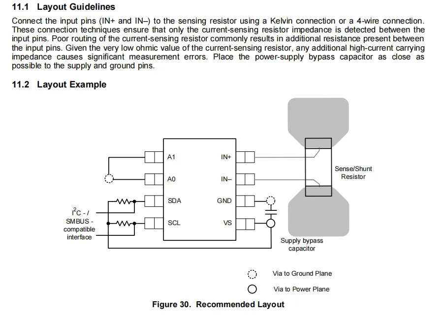
INA219 PCB Layout Requirements IN+ and IN- shall be connected to the sampling resistor via Kelvin four-wire connection to avoid measurement errors caused by additional impedance introduced by high-current traces; the power supply decoupling capacitor shall be placed close to the chip's power and ground pins, I²C bus shall be connected with pull-up resistors in series, and address pins, signals and power ground shall all be properly connected to the copper pour plane through vias to ensure sampling accuracy and stable bus communication.
III. Circuit Engineering
3.1 Circuit Source Engineering
To obtain the source code of the circuit, please follow the official account [Freak Embedded]
3.2 Module Usage Instructions
The schematic diagram of this module is shown below:
SCH_Schematic1_Current and Voltage Detection Module Based on INA219_v1.0.02026-05-07.pdf 2.4 MB
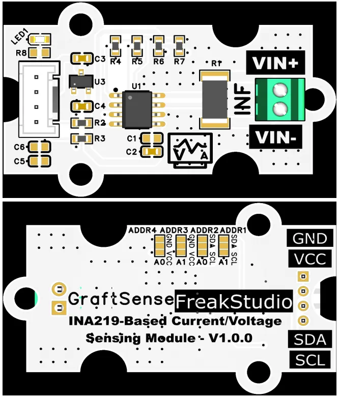
This module provides a IIC communication interface: it supports standard I2C communication rates, and can flexibly configure multiple I2C addresses via the address selection circuit consisting of A0 to A1, and is compatible with 3.3V level. Cooperating with the 16-bit ADC built in the INA219 chip, it can stably realize high-precision monitoring of bidirectional current, voltage and power, and the data can be directly read through the I2C bus. It is suitable for scenarios such as battery management, power supply monitoring, and DC system energy consumption monitoring, providing the system with reliable current and voltage Data Acquisition and interaction capabilities.
The physical device is equipped with a DB125-2.54-2P-GN-S terminal block, where the VIN+ terminal is connected to the high potential terminal (positive pole of the power supply) of the circuit under test, and the VIN- terminal is connected to the high potential terminal of the load / electrical appliance; that is, the module is connected in series in the test loop, so that the load current flows sequentially through VIN+, the sampling resistor R1, and VIN- to form a complete current path. In this way, the INA219 can measure the current, voltage and power based on the voltage drop across the sampling resistor.
The physical device has all A0, A1 address selection pins routed out. A0 and A1 pins can be selectively connected to one of the networks including GND, VCC, SDA, and SCL, so that multiple I2C communication addresses are selectable. Note that only one network can be connected to the three short-circuit points of the physical device's A0 and A1. The specific addresses are shown in the following figure:
3.3 Application Experiment
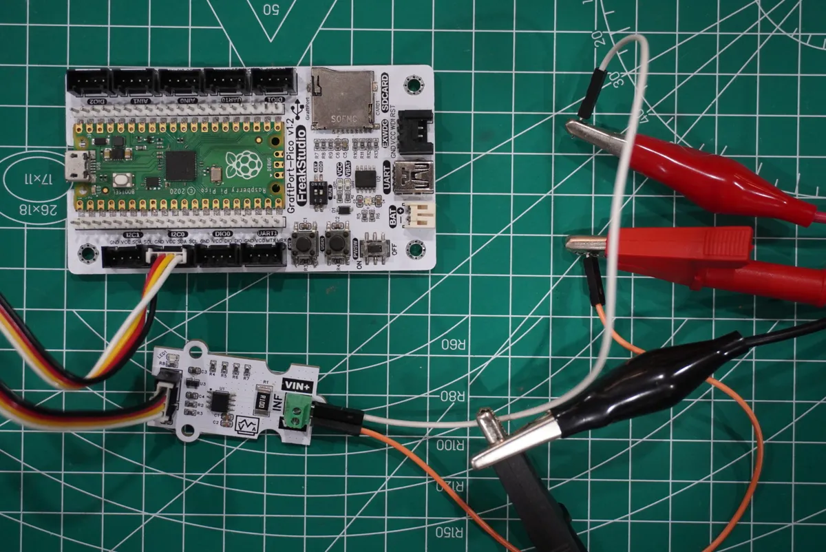
Here, we use the GraftPort-RP2040 development board for testing, and the INA219-based current and voltage detection module uses the I2C interface to communicate with the main controller.
Here, we first use the HY2.0-4P cable to connect the module to the GraftPort-RP2040 development board's I2C0 interface:
Development Board Pins | Module Pins | Description |
Pin 4 |
|
|
Pin 5 |
|
|
Test circuit wiring:
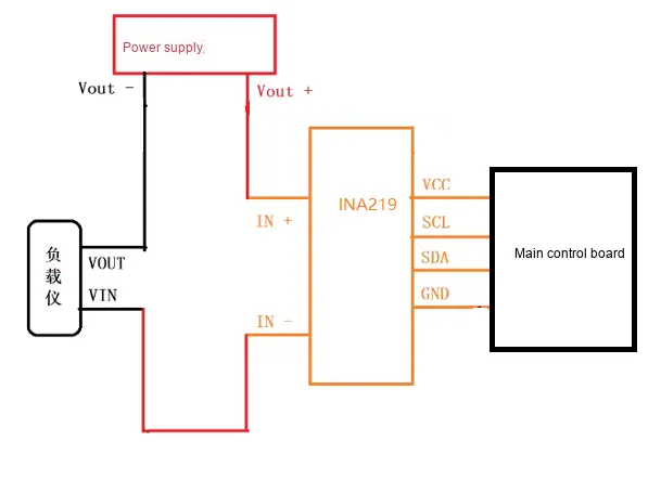
- Power supply output: Connect Vout+ to IN+ of the INA219, and connect Vout- to VOUT of the load instrument
- Load instrument wiring: Connect VIN to IN- of the INA226, and connect GND to the common ground of the system
- INA226 and the main control board: connect the VCC, SCL, SDA, and GND pins to the pins with the same labels on the main control board respectively.
| Connection start | Connection end |
|---|---|
| Power supply Vout + | INA226 IN + |
| INA226 IN - | Load tester VIN |
| Load tester VOUT | Power supply Vout - |
Here, we need to search for the relevant driver packages on uPyPI: https://upypi.net/zh/
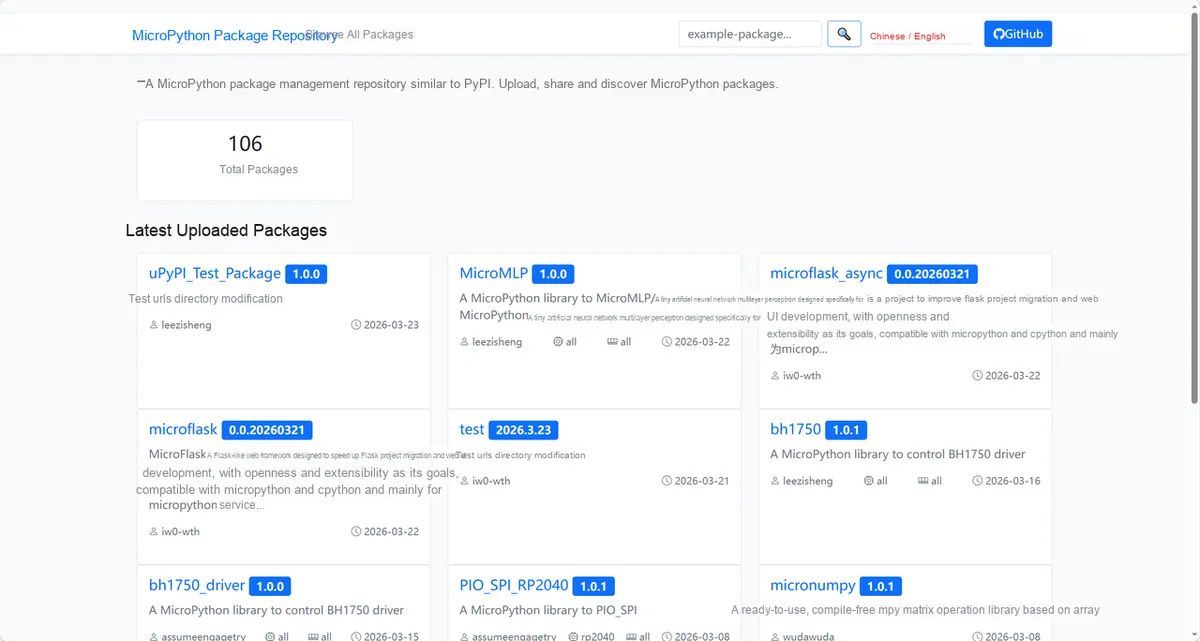
Enter ina219_driver to search, and the following will be displayed:
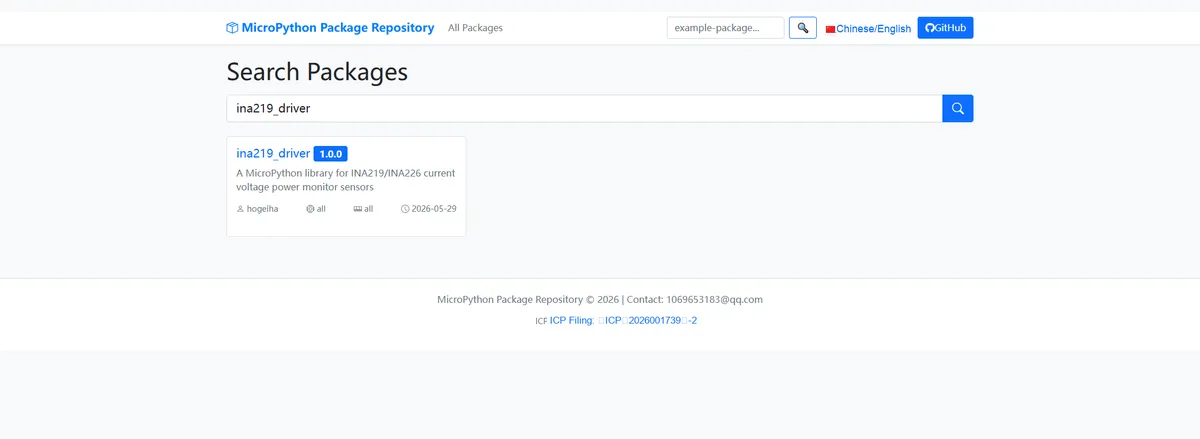
Click to copy the local installation command:
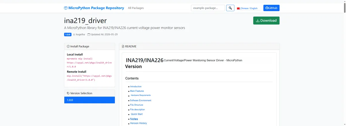
Import the module driver library code via the mip tool. Below are the usage commands for the mpremote tool:
mpremote mip install https://upypi.net/pkgs/ina219_driver/1.0.0Import the current and voltage detection module based on INA219 - MicroPython driver code, then copy the following main.py code into our project:
# Python env   : MicroPython v1.23.0
# -*- coding: utf-8 -*-
# @Time    : 2026/05/06 10:45
# @Author  : FreakStudio
# @File    : main.py
# @Description : Code to test the INA219 current, voltage and power monitoring driver
# @License : MIT


# ======================================== Import Modules =========================================

# Import the MicroPython hardware I2C and pin control modules
from machine import I2C, Pin

# Import the I2C bus adapter
from sensor_pack_2.bus_service import I2cAdapter

# Import the INA219 driver module
import ina_ti

# Import the time control module
import time


# ======================================== Global Variables ============================================

# I2C bus number
i2c_id = 0

# I2C data pin number
i2c_sda_pin = 4

# I2C clock pin number
i2c_scl_pin = 5

# I2C communication frequency (Hz)
i2c_freq = 400000

# INA219 default I2C address
ina219_addr = 0x40

# Commonly used shunt resistor value of the INA219 module (Ω)
shunt_resistance = 0.1

# Expected maximum measured current (A)
max_expected_current = 2.0

# Data print interval (seconds)
print_interval = 1000

# Timestamp of the last print (milliseconds)
last_print_time = 0


# ======================================== Functions ============================================


# ======================================== Custom Classes ============================================


# ======================================== Initialization ==========================================

# Wait for the system and sensor power to stabilize
time.sleep(3)

# Print the program function prompt
print("FreakStudio: Testing INA219 power monitor driver")

# Initialize the hardware I2C bus
i2c = I2C(
    i2c_id,
    sda=Pin(i2c_sda_pin),
    scl=Pin(i2c_scl_pin),
    freq=i2c_freq,
)

# Scan I2C bus devices
devices = i2c.scan()

# Check whether the scan result is empty
if not devices:
    raise RuntimeError("No I2C devices found on bus")

# Print the I2C device scan result
print("I2C devices found: %s" % [hex(addr) for addr in devices])

# Check whether the INA219 is on the I2C bus
if ina219_addr not in devices:
    raise RuntimeError("INA219 not found at address 0x%02X" % ina219_addr)

# Print the INA219 address confirmation
print("INA219 found at address: 0x%02X" % ina219_addr)

# Create the I2C adapter required by the driver
adapter = I2cAdapter(i2c)

# Create the INA219 sensor object
ina219 = ina_ti.INA219(
    adapter=adapter,
    address=ina219_addr,
    shunt_resistance=shunt_resistance,
)

# Set the bus voltage range to 16V (False=16V, True=32V)
ina219.bus_voltage_range = False

# Set the bus ADC to 12-bit resolution
ina219.bus_adc_resolution = 0x03

# Set the shunt ADC to 12-bit resolution
ina219.shunt_adc_resolution = 0x03

# Set the expected maximum measured current
ina219.max_expected_current = max_expected_current

# Start continuous measurement and write the calibration value
ina219.start_measurement(continuous=True, enable_calibration=True)

# Get the single-conversion wait time (microseconds)
wait_time_us = ina219.get_conversion_cycle_time()

# Print the current configuration register information
print("Configuration: %s" % str(ina219.get_config()))

# Print the conversion wait time
print("Conversion cycle time: %d us" % wait_time_us)


# ========================================  Main Program  ===========================================

try:
    while True:
        # Get the current timestamp
        current_time = time.ticks_ms()

        # Check whether the print interval has elapsed
        if time.ticks_diff(current_time, last_print_time) >= print_interval:
            # Wait for the sensor to complete one conversion
            time.sleep_us(wait_time_us)

            # Read the shunt voltage (V)
            shunt_voltage = ina219.get_shunt_voltage()

            # Read the bus voltage (V)
            bus_voltage = ina219.get_voltage()

            # Read the current (A)
            current = ina219.get_current()

            # Read the power (W)
            power = ina219.get_power()

            # Print the complete measurement results
            print("Bus: %.3f V, Shunt: %.6f V, Current: %.3f A, Power: %.3f W" % (
                bus_voltage, shunt_voltage, current, power
            ))

            # Update the last print time
            last_print_time = current_time

        # Short delay to avoid excessive CPU usage
        time.sleep_ms(10)


except KeyboardInterrupt:
    print("Program interrupted by user")
except OSError as e:
    print("Hardware communication error: %s" % str(e))
except Exception as e:
    print("Unknown error: %s" % str(e))
finally:
    print("Cleaning up resources...")
    # Release the INA219 object
    del ina219
    # Release the adapter object
    del adapter
    # Release the I2C object
    del i2c
    print("Program exited")
Burn the code, open the terminal, and the output is as follows:
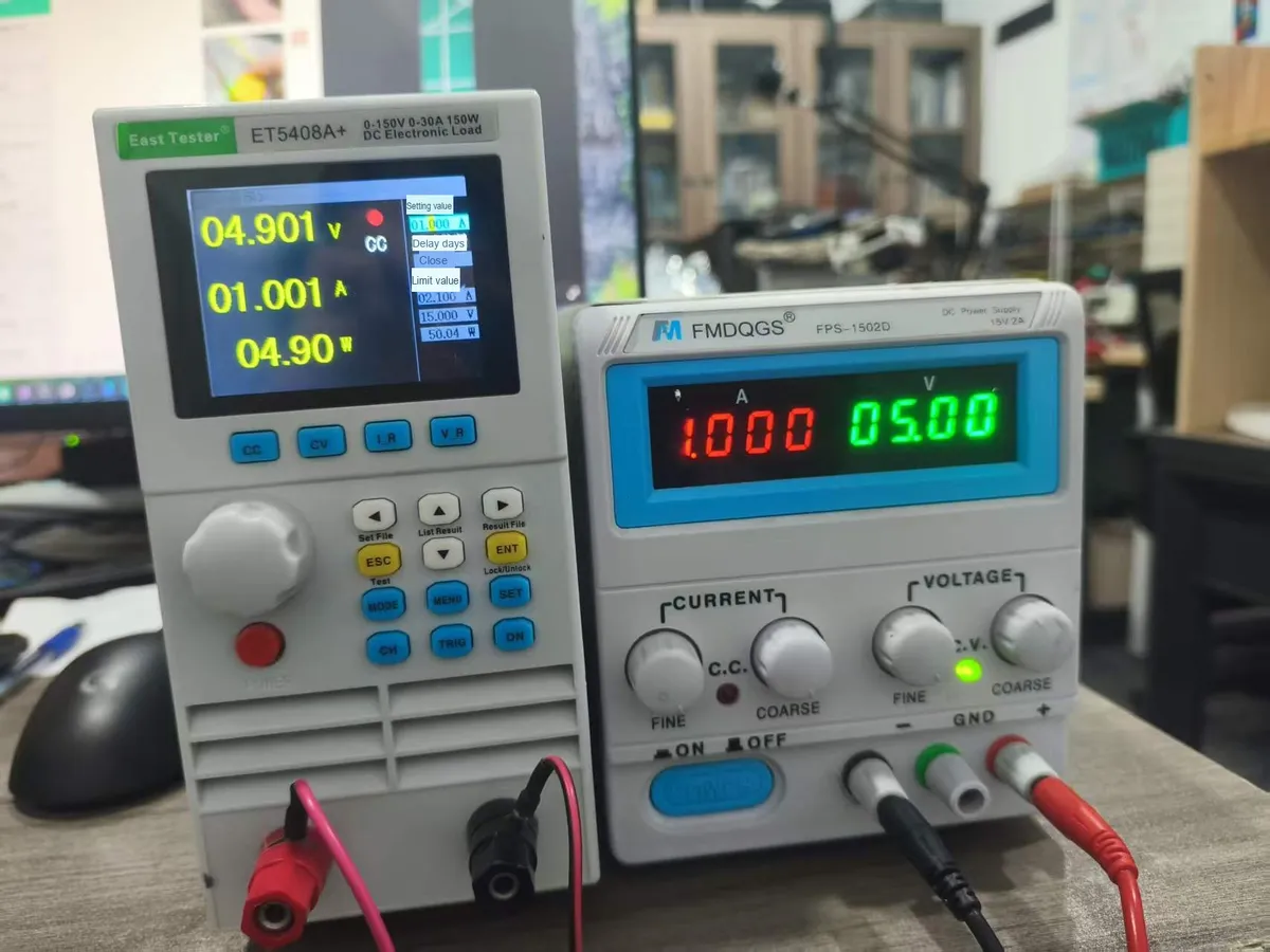
Compare and adjust the output values of the load instrument and the adjustable power supply.
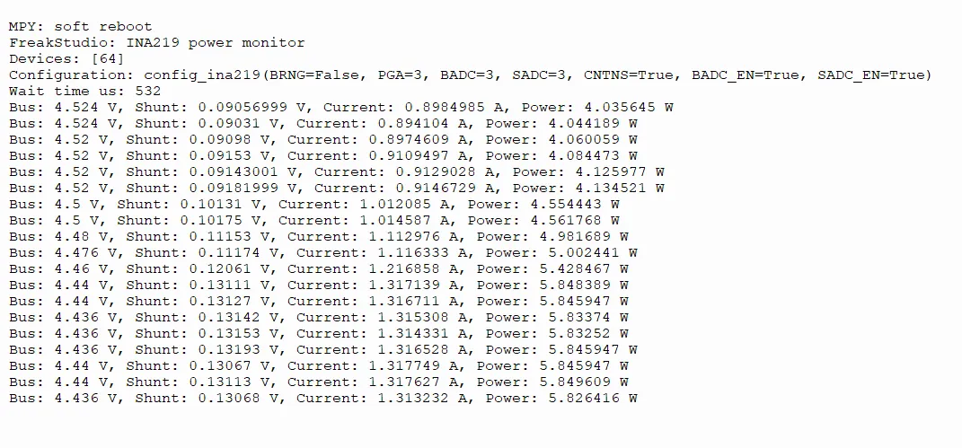
Here the parameters are set to 5V/1A, and the output is normal.
IV. Drivers
ina219_driver-1.0.0.zip 38 KB
5. BOM & Recommended Alternative Parts
None.
VI. Revision History
Document Version | Date Modified | Modifier | Modify Content |
v1.0 | 2026-05-07 | Ling Gaoxing | Initialize the document |
v1.1 | 2026-06-06 | Xin Ruili | Create an open version of the document based on the internal document version v1.0. |
7. Relevant Materials
7.1 Chip Datasheet
ina219.pdf 1.1 MB
7.2 Unique Icons for PCB Silk Screen