Contents
- I. Module Introduction
- II. Introduction to Main Chips
- 2.1 Chip Overview
- 2.2 Pin Definition
- 2.3 Functional Block Diagram
- 2.4 Performance Parameters
- 2.5 Reference Circuit
- 2.6 Chip Configuration
- 2.7 Communication Interfaces and Related Protocols
- 2.8 PCB Routing Precautions
- III. Circuit Engineering
- 3.1 Circuit Source Engineering
- 3.2 Module Usage Instructions
- 3.3 Application Experiment
- IV. Drivers
- 5. BOM & Recommended Alternative Parts
- VI. Revision History
- 7. Relevant Materials
- 7.1 Chip Datasheet
- 7.2 Unique Icons for PCB Silk Screen
I. Module Introduction
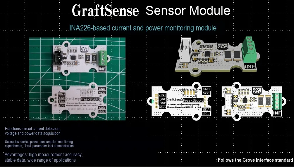
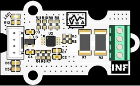
Current and Power Monitoring Module Based on INA226, which adopts the INA226 high-precision current/voltage/power monitoring chip solution, realizes bidirectional current, voltage and power measurement through the I2C interface. Built with a 16-bit ADC, it can directly read the bus voltage and shunt voltage and automatically calculate the real-time current and power; the module supports monitoring of 0~36V DC systems, can adapt to multiple current ranges with different sampling resistors, and is also equipped with programmable alarm pins to realize abnormal reminders such as over-current, over-voltage and over-power;Equipped with address selection circuit, LDO voltage regulator circuit, power filtering and indicator circuit, it is powered by 3.3V, with an operating voltage range of 2.7~5.5V, featuring high precision and low power consumption, and is suitable for scenarios such as power management, battery monitoring, and energy consumption monitoring of industrial equipment.
II. Introduction to Main Chips
INA226 is TI 's 16-bit high-precision I2C interface monitoring chip , supporting 0~ 36V bus voltage, bidirectional current and power measurement, with alarm function, 2.7~ 5.5V power supply.
2.1 Chip Overview
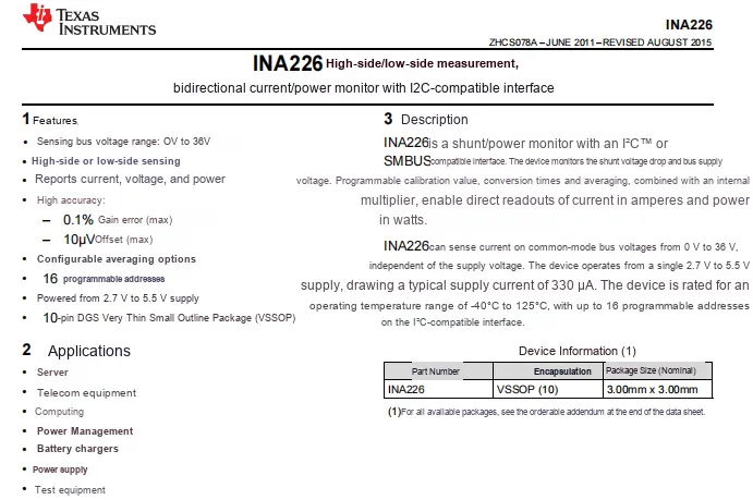
INA226 features an I²C / SMBus compatible interface, supports high-side/low-side current sensing for bus voltages from 0 to 36V, can directly output current, voltage and power values, with an accuracy of 0.1% gain error and a maximum offset of 10μV, supports configurable average sampling and 16 programmable addresses, is powered by a single 2.7V~5.5V supply, and comes in a VSSOP-10 package, making it suitable for applications such as servers, power management, and battery chargers.
2.2 Pin Definition
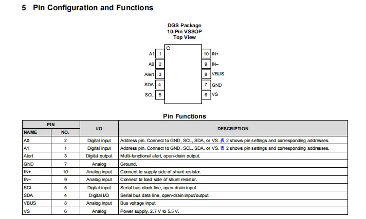
The pins are categorized into four types: address configuration, bus interface, power supply, and sampling input, among which A0 and A1 are used to set the slave address, Alert is an open-drain alarm output, SDA and SCL serve as I2C open-drain data and clock lines, VS is the power supply input for the chip, VBUS is the bus voltage sampling terminal, and IN+ and IN- are respectively connected to both ends of the shunt resistor to detect the voltage drop; during layout and wiring, priority shall be given to ensuring that the traces from IN+ and IN- to the sampling resistor are short and paired, so as to reduce measurement errors caused by additional copper foil voltage drops.
2.3 Functional Block Diagram
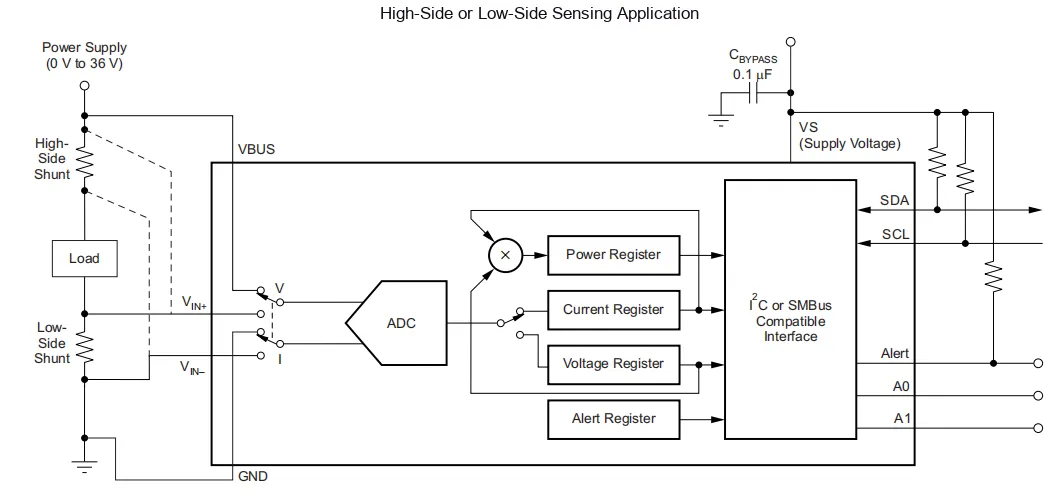
The INA226 can acquire voltage signals through a high-side or low-side shunt resistor;the VBUS pin collects the bus voltage. After the two signals are converted by the ADC, they are stored in the voltage register and current register respectively. The power is then calculated by a multiplier and stored in the power register, and the data is finally output via the I²C / SMBus interface. It also supports configuring the alarm function through the Alert register;the VS pin is powered by a 2.7~5.5V power supply and decoupled via a 0.1μF capacitor, while the A0 / A1 pins can configure the communication address to realize bus mounting.
2.4 Performance Parameters
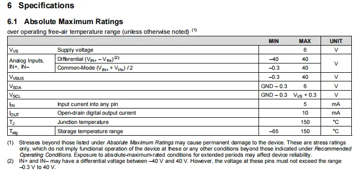
The absolute maximum ratings indicate that VS has a supply upper limit of 6V, the absolute input range of VBUS is from -0.3V to 40V, the absolute differential input range between IN+ and IN- is from -40V to 40V, and the storage temperature range is from -65°C to 150°C; these parameters are used for device boundary constraints and shall not be directly used as long-term operating conditions.
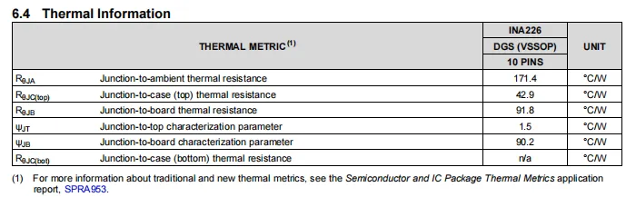
The thermal characteristics table provides the thermal resistance parameters for the 10-pin VSSOP package, RθJA has a typical value of 171.4°C/W, which indicates that although the power consumption of the chip itself is not high, it is still necessary to avoid placing large-area heat sources in close proximity; during module design, the high-current shunt resistor should be properly isolated from the chip body.
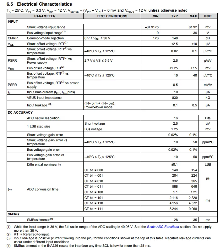
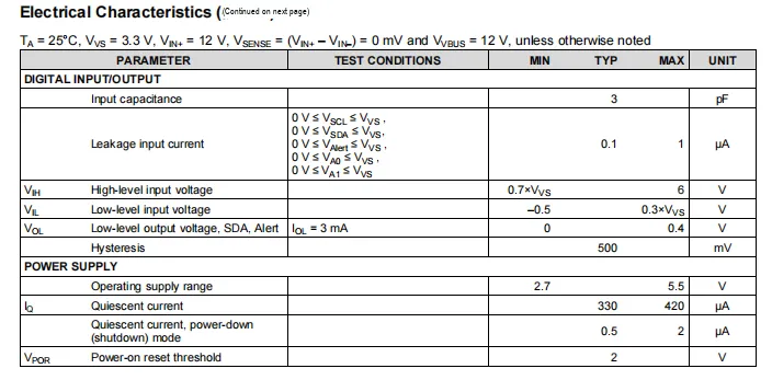
INA226 electrical characteristics under 25℃ and 3.3V supply: shunt voltage input range ±81.92mV, maximum bus voltage 36V, 16-bit ADC resolution corresponding to shunt voltage LSB of 2.5μV, bus voltage LSB of 1.25mV, maximum gain error 0.1%, conversion time adjustable from 140μs to 9.068ms depending on configuration;The parameters of the digital interface include input capacitance, leakage current and high/low level thresholds, with a power supply Scope of Work of 2.7~5.5V, a typical operating current of 330μA, and a current as low as 0.5μA in shutdown mode.
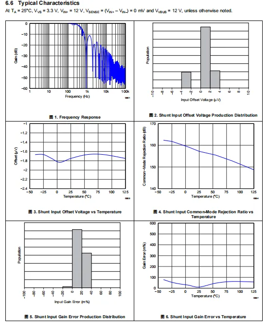
INA226 The typical characteristic curves, covering the frequency response, production distribution and temperature characteristics of input offset voltage, common-mode rejection ratio versus temperature, as well as the production distribution and temperature characteristics of shunt input gain error, demonstrate the chip's performance under different frequency and temperature conditions and its production consistency data.
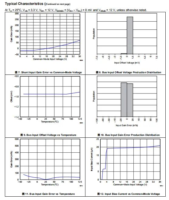
INA226 under the supply conditions of 25℃ and 3.3V: it intuitively presents the accuracy, consistency and temperature stability of the chip under different working conditions, covering the variation of shunt input gain error with common-mode voltage, the production distribution and temperature characteristics of bus input offset voltage and gain error, as well as the curve of input bias current varying with common-mode voltage.
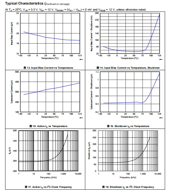
INA226 current characteristics: including the variation of input bias current and quiescent current with temperature in operation/shutdown modes, as well as the variation of quiescent current with I²C clock frequency in both modes, which intuitively presents the power consumption performance and current stability of the chip under different temperatures and communication rates.
2.5 Reference Circuit
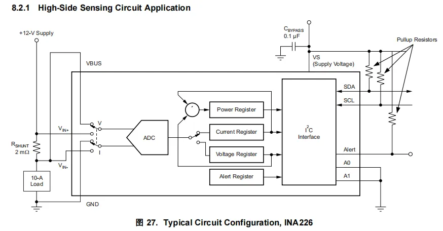
A 12V power supply feeds a 10A load via a 2mΩ sense resistor, and the chip acquires the differential voltage across the sense resistor through the VIN+ / VIN- pins, while collecting the bus voltage via the VBUS pin; after being converted by the ADC, the signals are stored in the current and voltage registers respectively, then the power is calculated by a multiplier and stored in the power register, and finally the data is output via the I²C interface;A 0.1μF capacitor at the power supply terminal is used for decoupling, SDA / SCL / Alert pins are connected with pull-up resistors, and the A0 / A1 pins are grounded to configure the I²C address, enabling high-precision current, voltage and power monitoring.
2.6 Chip Configuration
None.
2.7 Communication Interfaces and Related Protocols
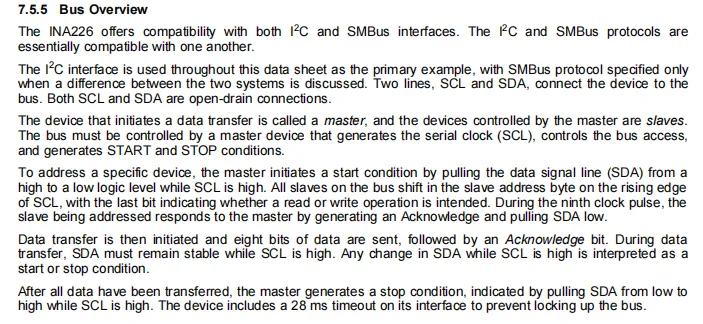
INA226 's I²C interface: the chip acts as a slave, communicates with the master via two open-drain lines SCL and SDA, and complies with the standard I²C protocol. The master implements read and write operations through the start condition, slave address (including read/write bit), data transmission and stop condition, and a built-in 28ms timeout mechanism is also integrated to prevent bus hang-up.
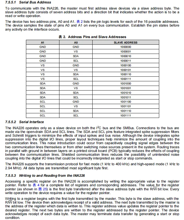
INA226, as an I²C slave, implements 16 programmable addresses via different level combinations of the A0 and A1 pins (which can be connected to GND, VS, SDA, and SCL); the SDA / SCL pins integrate spike suppression and Schmitt triggers, support fast (400kHz) and high-speed (2.94MHz) modes, and transmit data with the most significant bit first. For read and write operations, the slave address (including the read/write bit) must be sent first; for write operations, the register pointer must be sent before writing data, while for read operations, the register pointer must be configured before initiating a read command.
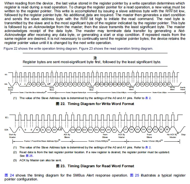
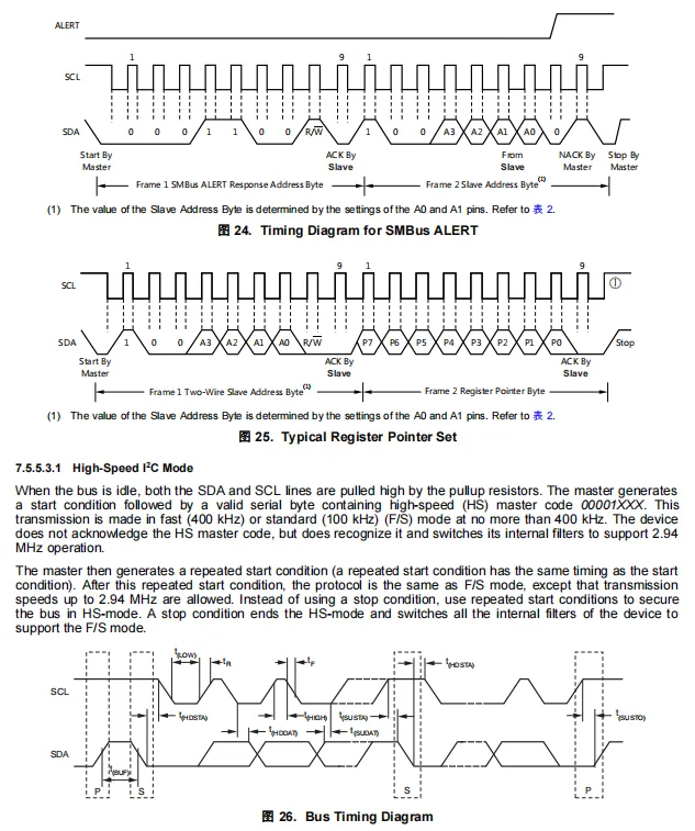
For write operations, the slave address and register pointer shall be sent first, followed by two data bytes written in high-byte-first order; for read operations, the register pointer shall be written first, then a read command is initiated with a repeated start to receive the high and low byte data sent by the slave; in addition, this document also includes SMBus alert response timing, register pointer configuration procedure, and high-speed I²C mode (max. 2.94MHz) bus timing description.
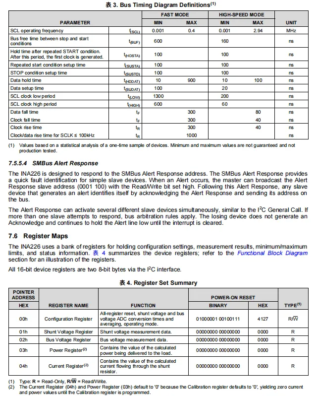
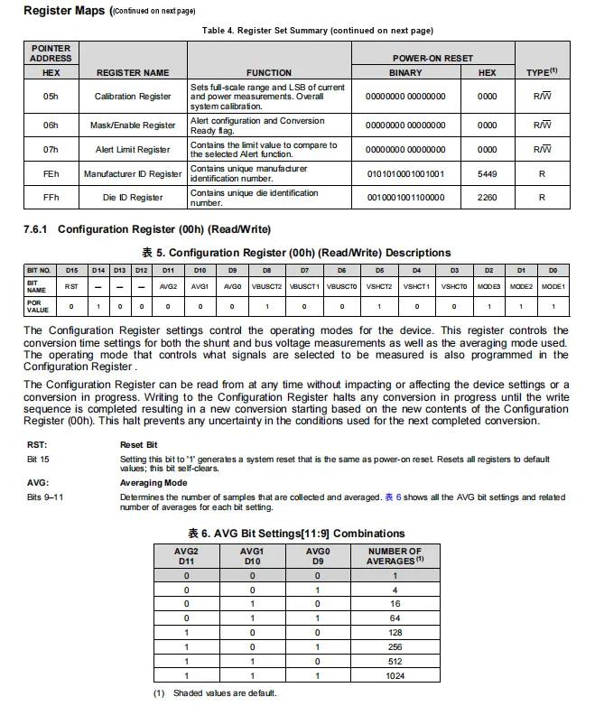
The I²C/SMBus bus timing parameters and SMBus alert response mechanism are covered, along with a complete register map listing all registers spanning configuration, shunt/bus voltage, current, power, calibration, alert configuration, and manufacturer/chip ID. The document also specifies the system reset of configuration registers, number of sampling averages, conversion time, and operating mode settings, providing a comprehensive configuration and communication basis for the chip's high-precision current, voltage and power measurement.
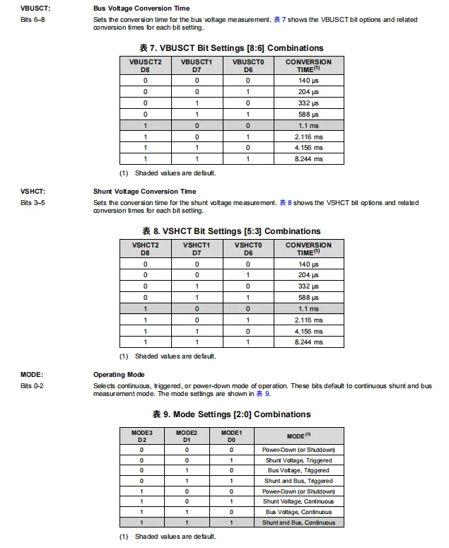
VBUSCT (bits 6-8) sets the bus voltage conversion time, ranging from 140μs to 8.244ms;VSHCT (bits 3-5) sets the shunt voltage conversion time, ranging from 140μs to 8.244ms;MODE (bits 0-2) selects the operating mode, including power-down, single-trigger, continuous measurement, etc. The default is the continuous measurement mode for shunt and bus voltage, which is used to configure the measurement speed, power consumption and operating mode.
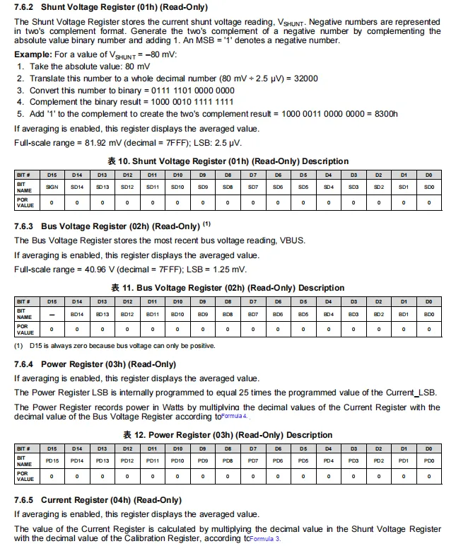
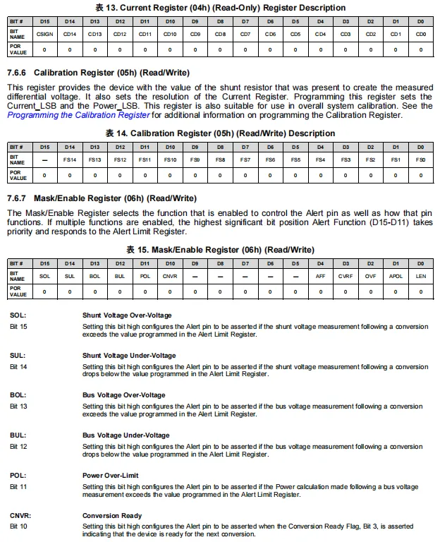
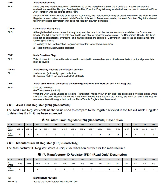
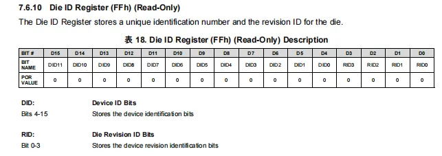
The shunt voltage, bus voltage, current and power registers are read-only measurement data registers, corresponding to an LSB of 2.5μV and 1.25mV respectively; the current/power data are valid only after the calibration registers are configured. The calibration registers are used to set the sampling resistance value and the current/power resolution. The alarm-related registers (Mask / Enable, Alert Limit) can configure alarm conditions such as overvoltage, undervoltage, overcurrent, and power over-limit. Finally, there are also read-only manufacturer ID and chip ID registers, which are used to identify the device model and version.
2.8 PCB Routing Precautions
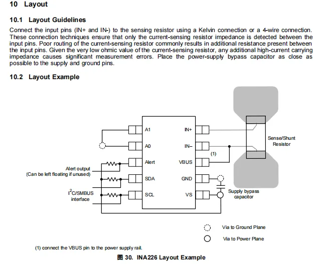
Connect IN+ / IN- to the sampling resistor using the Kelvin (four-wire) method to prevent additional trace resistance from affecting measurement accuracy;VBUS connects directly to the power rail, and a power supply decoupling capacitor shall be placed close to the VS pin;SDA / SCL require pull-up resistors, the Alert pin can be externally pulled up or left floating, and the address pins A0 / A1 are configured as required, and connected to the power/ground plane through vias to ensure signal integrity and measurement accuracy.
III. Circuit Engineering
3.1 Circuit Source Engineering
To obtain the source code of the circuit, please follow the official account [Freak Embedded]
3.2 Module Usage Instructions
The schematic diagram of this module is shown below:
SCH_Schematic1_Current and Power Monitoring Module Based on INA226_v1.0.0_2026-05-08.pdf 2.3 MB
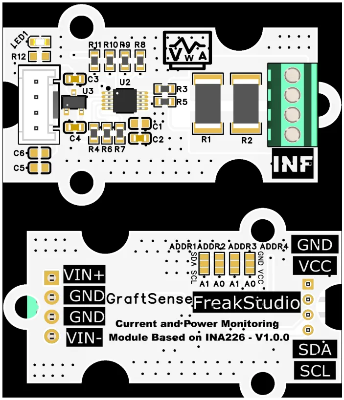
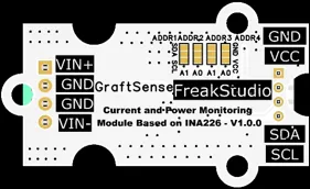
This module provides an IIC communication interface: it supports standard I2C communication rates, and can flexibly configure multiple ADDR1 - ADDR4 I2C addresses via short-circuiting, is compatible with 3.3V/5V logic levels, and can stably transmit the bidirectional current, voltage and power digital signals collected by I2C addresses, is compatible with 3.3V/5V levels, and can stably transmit the bidirectional current, voltage and power digital signals collected by INA226. It is applicable to scenarios such as power management, battery monitoring, and industrial equipment energy consumption monitoring, providing the system with reliable and high-precision power monitoring data interaction capabilities.
The physical device is equipped with a DB125-2.54-4P-GN-S terminal block, where the VIN + terminal connects to the high-potential terminal (positive pole of the power supply) of the circuit under test, and the VIN - terminal connects to the high-potential terminal of the load / electrical appliance. That is to say, the module is connected in series in the test loop, so that the load current flows sequentially through VIN+, the sampling resistors R1 / R2, and VIN- to form a complete current path. In this way, the INA226 can measure current, voltage and power based on the voltage drop across the sampling resistors.
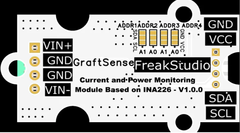
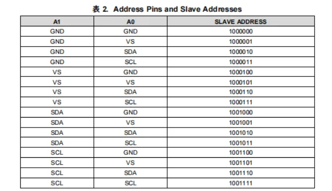
The physical device has all A0, A1 address selection pins routed out. A0 and A1 pins can be selectively connected to one of the networks including GND, VCC, SDA, and SCL, so that multiple I2C communication addresses are selectable. Note that only one network can be connected to the three short-circuit points of the physical device's A0 and A1. The specific addresses are shown in the following figure:
3.3 Application Experiment
Here, we use the GraftPort-RP2040 development board for testing, and the INA226-based current and power monitoring module communicates with the main controller via the I2C interface.
Here, we first use the HY2.0-4P cable to connect the module to the GraftPort-RP2040 development board's I2C0 interface:
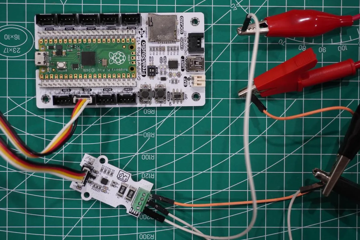
Development Board Pins | Module Introduction | Description |
Pin 4 |
|
|
Pin 5 |
|
|
Measurement circuit wiring:
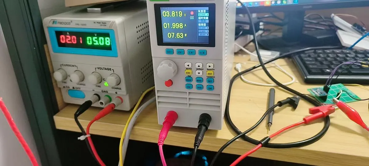
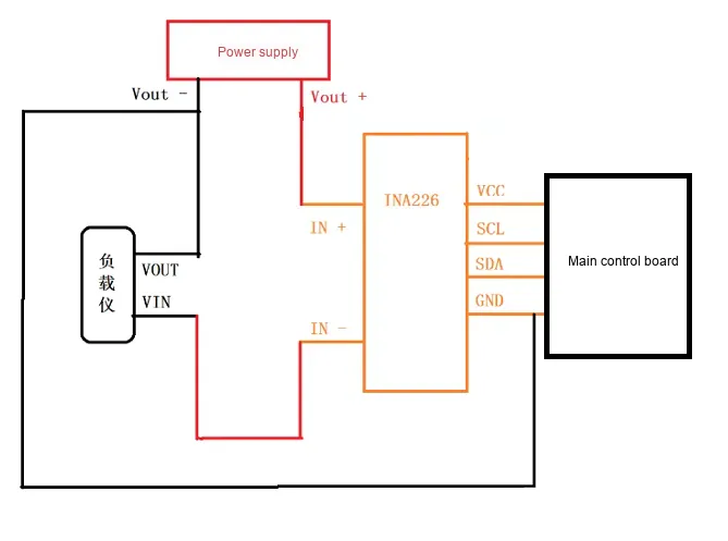
- Power supply output: Connect Vout+ to IN+ of the INA226, and connect Vout- to VOUT of the load instrument
- Load instrument wiring: Connect VIN to IN- of the INA226, and connect GND to the common ground of the system
- INA226 and the main control board: connect the VCC, SCL, SDA, and GND pins to the pins with the same labels on the main control board respectively.
| Connection start | Connection end |
|---|---|
| Power supply Vout + | INA226 IN + |
| INA226 IN - | Load tester VIN |
| Load tester VOUT | Power supply Vout - |
| Power supply Vout - | INA226 GND |
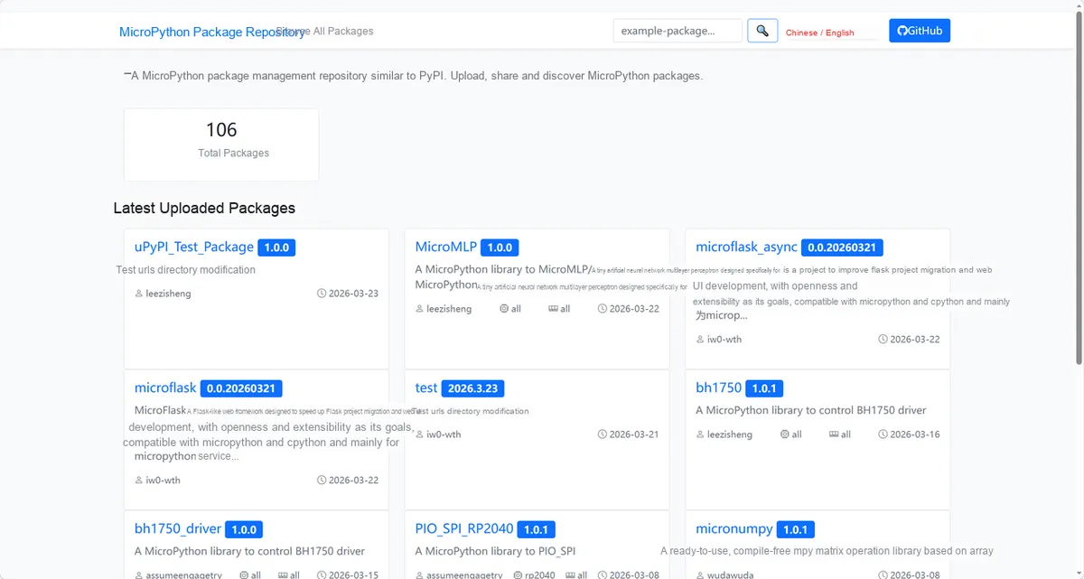
Here, we need to search for the relevant driver packages on uPyPI: https://upypi.net/zh/
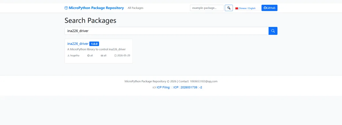
Enter ina226_driver to search, and the following will be displayed:
Click to copy the local installation command:
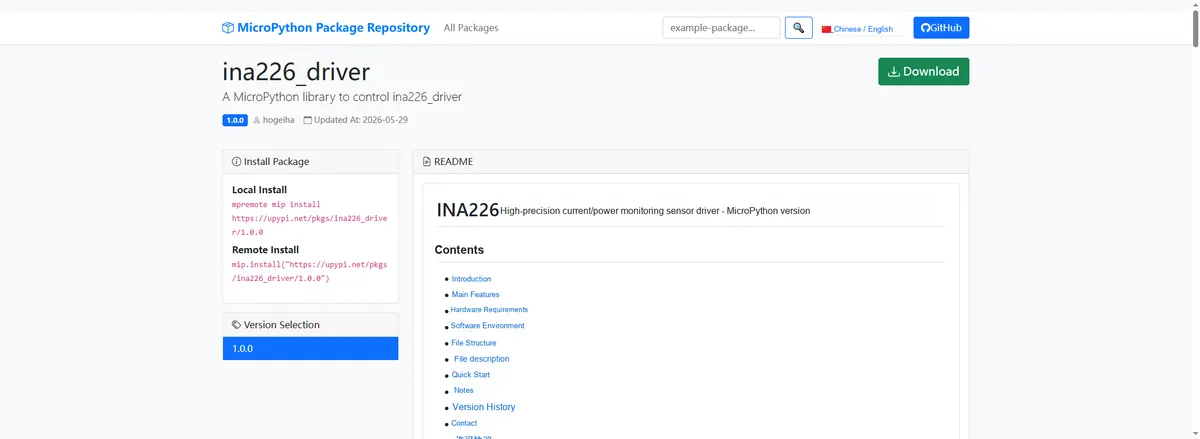
Import the module driver library code via the mip tool. Below are the usage commands for the mpremote tool:
mpremote mip install https://upypi.net/pkgs/ina226_driver/1.0.0Import the MicroPython driver code for the INA226-based current and power monitoring module, then copy the following main.py code into our project:
# Python env   : MicroPython v1.23.0
# -*- coding: utf-8 -*-
# @Time    : 2026/4/16 PM 2:30
# @Author  : hogeiha
# @File    : main.py
# @Description : INA226 current/power sensor I2C scan and measurement example

# ======================================== Import Modules =========================================

import time
from machine import Pin, SoftI2C
from sensor_pack_2.bus_service import I2cAdapter
import ina_ti

# ======================================== Global Variables ============================================

# ======================================== Functions ============================================


# Display the section title
def show_header(info: str, width: int = 32):
    print(width * "-")
    print(info)
    print(width * "-")


# Microsecond-level delay
def my_sleep(delay_us: int):
    time.sleep_us(delay_us)


# ======================================== Custom Classes ============================================

# ======================================== Initialization configuration ===========================================

if __name__ == "__main__":
    # Wait 3 seconds before starting to ensure the peripherals are stable
    time.sleep(3)
    # Print the debug identifier
    print("FreakStudio: INA226 sensor initialization")

    # Automatically identify the sensor address, define a global target address list (supports multiple addresses; use [] even for a single one)
    TARGET_SENSOR_ADDRS = [0x40]  # INA226 default address

    # I2C initialization (compatible with I2C/SoftI2C)
    i2c_bus = SoftI2C(sda=Pin(4), scl=Pin(5), freq=100000)

    # Start scanning for devices on the I2C bus
    devices_list: list[int] = i2c_bus.scan()
    print("START I2C SCANNER")

    # Check the I2C device scan result
    if len(devices_list) == 0:
        print("No i2c device !")
        raise SystemExit("I2C scan found no devices, program exited")
    else:
        print("i2c devices found:", len(devices_list))

    # Iterate over the address list to initialize the target sensor
    sensor = None  # Placeholder for the sensor object initialization
    for device in devices_list:
        if device in TARGET_SENSOR_ADDRS:
            print("I2c hexadecimal address:", hex(device))
            try:
                # Automatically identify and initialize the corresponding sensor
                adaptor = I2cAdapter(i2c_bus)
                sensor = ina_ti.INA226(adapter=adaptor, address=device, shunt_resistance=0.01)
                sensor.shunt_voltage_enabled = True
                sensor.max_expected_current = 2.0  # Ampere
                print("Sensor initialization successful")
                break
            except Exception as e:
                print(f"Sensor Initialization failed: {e}")
                continue
    else:
        # Target device not found, raise an exception
        raise Exception("No target sensor device found in I2C bus")

    # ========================================  Main Program  ============================================

    # Number of measurement loops
    cycles_count = 10

    # Manual measurement mode
    show_header("INA226. Manual mode with settings")
    # Start a single measurement (non-continuous mode) and perform calibration
    sensor.start_measurement(continuous=False, enable_calibration=True)
    # Print the configuration register value
    print(f"configuration: {sensor.get_config()}")
    # Get the conversion cycle time (microseconds)
    wait_time_us = sensor.get_conversion_cycle_time()
    print(f"wait_time_us: {wait_time_us} us.")
    # Measurement loop
    for _ in range(cycles_count):
        # Wait 100 ms
        time.sleep_ms(100)
        # Wait for the conversion to complete
        my_sleep(wait_time_us)
        # Get the data status
        ds = sensor.get_data_status()
        # If the conversion is not ready, skip this iteration
        if not ds.conv_ready_flag:
            print(f"data status: {ds}")
            continue
        # Read shunt voltage, bus voltage, current, and power
        shunt_v, bus_v, curr, pwr = sensor.get_shunt_voltage(), sensor.get_voltage(), sensor.get_current(), sensor.get_power()
        print(f"Shunt: {shunt_v} V;\tBus: {bus_v}\tCurrent: {curr}\tpower: {pwr}")
        # Disable repeated calibration (no calibration each time a measurement is triggered manually)
        sensor.start_measurement(continuous=False, enable_calibration=False)

    # Automatic measurement mode
    show_header("INA226. Automatic continuous mode")
    # Start continuous measurement mode and perform calibration
    sensor.start_measurement(continuous=True, enable_calibration=True)
    # Print the configuration register value
    print(f"configuration: {sensor.get_config()}")
    # Iterate over sensor data (automatic measurement mode supports iteration)
    for data in sensor:
        # Wait for the conversion to complete
        my_sleep(wait_time_us)
        # Get the data status
        ds = sensor.get_data_status()
        # If the conversion is not ready, skip this iteration
        if not ds.conv_ready_flag:
            print(f"data status: {ds}")
            continue
        # Print the measurement data, current, and power
        print(f"data: {data}, current: {sensor.get_current()}, pwr: {sensor.get_power()}")
        # Delay 100 ms to avoid blocking the IDE
        time.sleep_ms(500)
Burn the code, open the terminal, and the output is as follows:
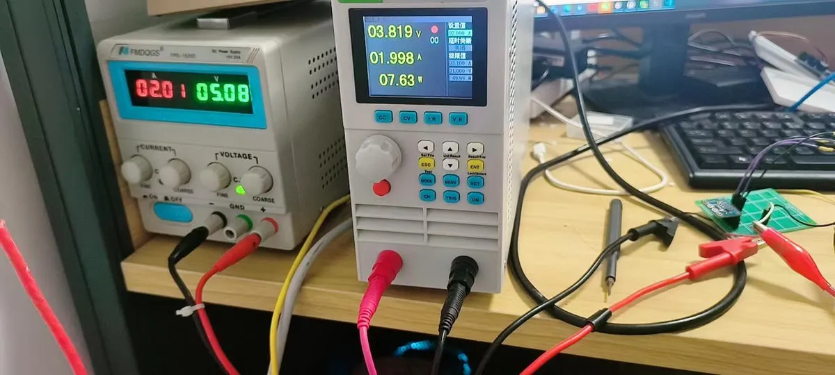
Compare the output values of the load tester and the adjustable power supply:
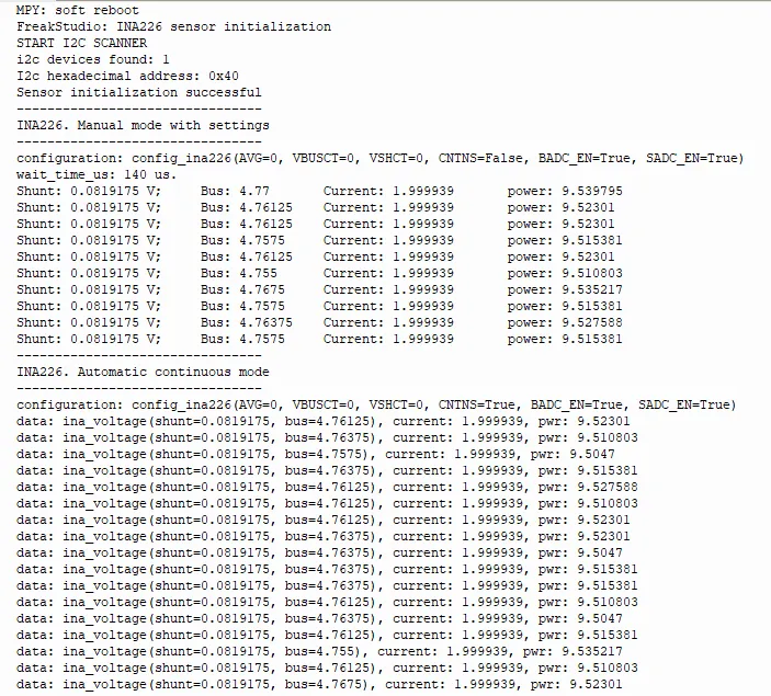
Here, the parameter is a 4.7V 2A constant current load, and the output is normal.
IV. Drivers
ina226_driver-1.0.0.zip 44 KB
5. BOM & Recommended Alternative Parts
None.
VI. Revision History
Document Version | Date Modified | Modifier | Modify Content |
v1.0 | 2026-05-08 | Ling Gaoxing | Initialize the document |
v1.1 | 2026-06-06 | Xin Ruili | Create an open version of the document based on the internal document version v1.0. |
7. Relevant Materials
7.1 Chip Datasheet
INA226.pdf 1.1 MB
7.2 Unique Icons for PCB Silk Screen