Contents
- I. Module Introduction
- II. Introduction to Main Chips
- 2.1 Chip Overview
- 2.2 Pin Definition
- 2.3 Functional Block Diagram
- 2.4 Performance Parameters
- 2.5 Reference Circuit
- 2.6 Chip Configuration
- 2.7 Communication Interfaces and Related Protocols
- 2.8 PCB Routing Precautions
- III. Circuit Engineering
- 3.1 Circuit Source Engineering
- 3.2 Module Usage Instructions
- 3.3 Application Experiment
- IV. Drivers
- 5. BOM & Recommended Alternative Parts
- VI. Revision History
- VII. Relevant Materials
- 7.1 Chip Datasheet
- 7.2 Unique Icons for PCB Silk Screen
I. Module Introduction
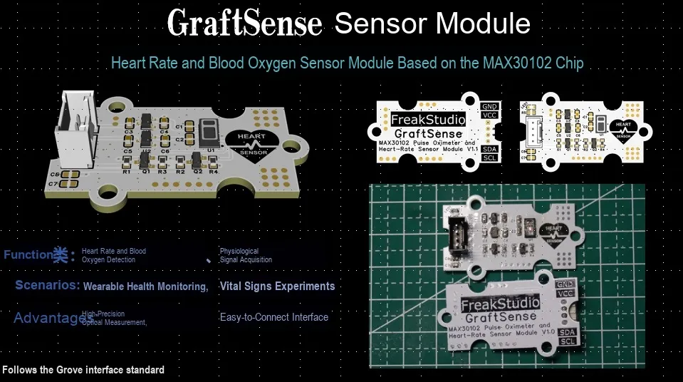
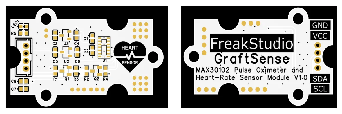
Heart rate and blood oxygen sensor module based on the MAX30102 chip, designed with the MAX30102EFD+ T sensor, communicates with the microcontroller via I2C. The operating voltage of the chip is + 1.8V, with a typical operating current of 600μA (maximum 1200μA).It leverages red light and infrared light to penetrate the skin and blood, and by detecting the difference in absorption of light at different wavelengths by hemoglobin (Hb) and oxyhemoglobin (HbO₂), it outputs a digital signal through preamplification, filtering, and ADC conversion, achieving accurate measurement of heart rate and blood oxygen. It is suitable for scenarios such as health monitoring and wearable devices, and provides reliable hardware support for physiological parameter detection.
II. Introduction to Main Chips
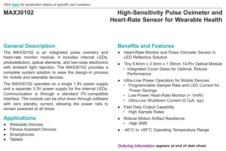
MAX30102EFD+ T is a high-precision pulse oximeter and heart rate sensor integrated with infrared, red light and dual infrared, featuring a built-in low-noise optical receiver and LED driver circuit. It supports the detection of heart rate, blood oxygen saturation (SpO₂) and respiratory rate, with a wide measurement range and high accuracy.It communicates with the main controller via the I²C interface, supports a supply voltage of 1.8~3.3V, features a low-power mode (with a standby current of only 0.7μA), has built-in ambient light suppression algorithm and temperature compensation function, delivers strong anti-interference performance, adopts a compact 2.5mm×4.4mm×1.0mm package, and is compliant with the RoHS standard. It is widely used in wearable medical and consumer electronics scenarios such as smart bracelets, watches, and health monitoring devices.
2.1 Chip Overview
2.2 Pin Definition
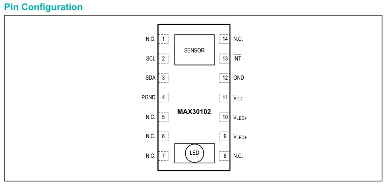
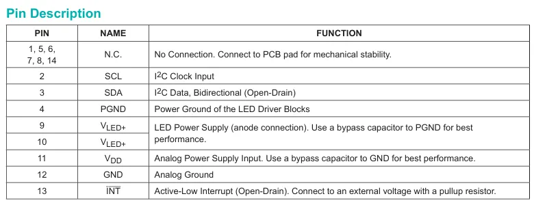
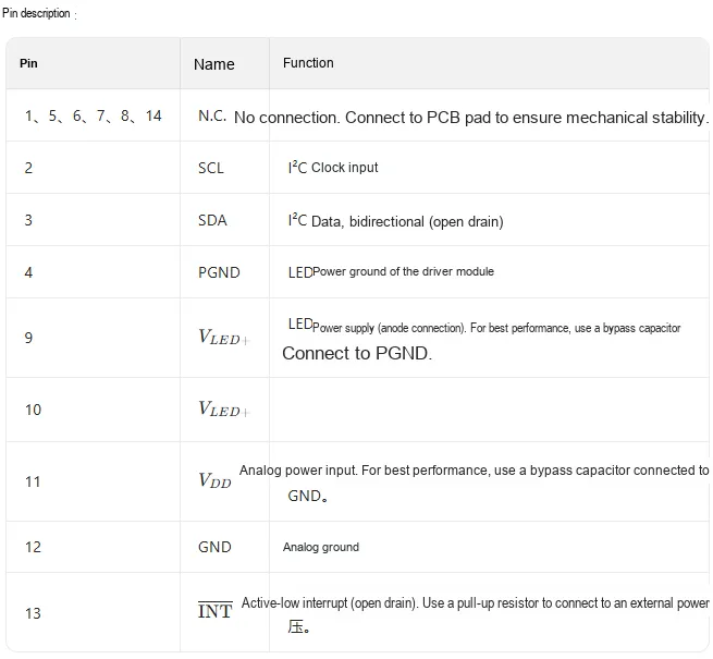
2.3 Functional Block Diagram
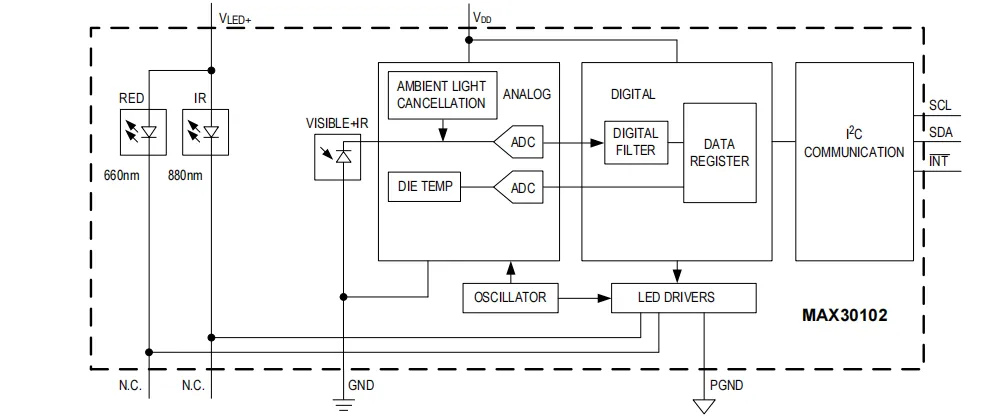
MAX30102EFD+ T is a complete pulse oximeter and heart rate monitoring system solution module, designed for the stringent requirements of wearable devices. This device maintains an extremely small solution size without compromising optical or electrical performance. It requires very few external hardware components for integration into wearable systems. The following is the functional block diagram description of MAX30102EFD+ T:
- LED Emitter Module (RED 660nm, IR 880nm)
- It emits 660nm red light and 880nm infrared light respectively, which penetrate human skin tissue and are then absorbed and reflected by blood, providing a light source for heart rate and blood oxygen saturation detection.
- Optical Receiving and Analog Processing Module (VISIBLE+ IR, AMBIENT LIGHT CANCELLATION, ADC, DIE TEMP)
VISIBLE+ IRPhotodiode: Receives the red light and infrared light reflected by the human body and converts them into electrical signals.- Ambient Light Elimination Unit: Filters out ambient light interference to improve signal purity.
ADC(Analog-to-Digital Converter): converts analog electrical signals into digital signals; meanwhile, it collects the chip temperature (DIE TEMP) and converts it into a digital signal for temperature compensation.
- Digital Processing Module (
DIGITAL FILTER, DATA REGISTER)- Digital filter: filters the digital signal output by the ADC to remove noise; the data register is used to temporarily store the processed data such as heart rate and blood oxygen saturation.
- Oscillation and LED Driver Modules (OSCILLATOR, LED DRIVERS)
Detailed Description:
MAX30102EFD+ Tintegrates red and infrared LED drivers to modulate LED pulses for blood oxygen and heart rate measurement. The LED current can be programmed from 0 to 50mA at an appropriate supply voltage. The LED pulse width can be programmed between 69μs and 411μs, enabling the algorithm to optimize the accuracy and power consumption of blood oxygen and heart rate according to the usage scenario.Working Principle: The oscillator generates a clock signal to control the operating timing of the LED driving module, so that the LED emits optical signals at the set frequency.
Typical Scenario (Taking Heart Rate and Blood Oxygen Detection as an Example):
- Transmission: The oscillator controls the LED drive module → causing the RED and IR LEDs to emit optical signals of corresponding wavelengths, which penetrate the human skin.
- Reception and Processing: The reflected light is received by the VISIBLE+ IR photodiode and converted into an electrical signal → after ambient light elimination and ADC conversion, it becomes a digital signal → processed by a digital filter and temporarily stored in the data register → the main controller reads the data via the I²C interface to calculate the heart rate and blood oxygen saturation.
2.4 Performance Parameters
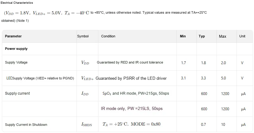
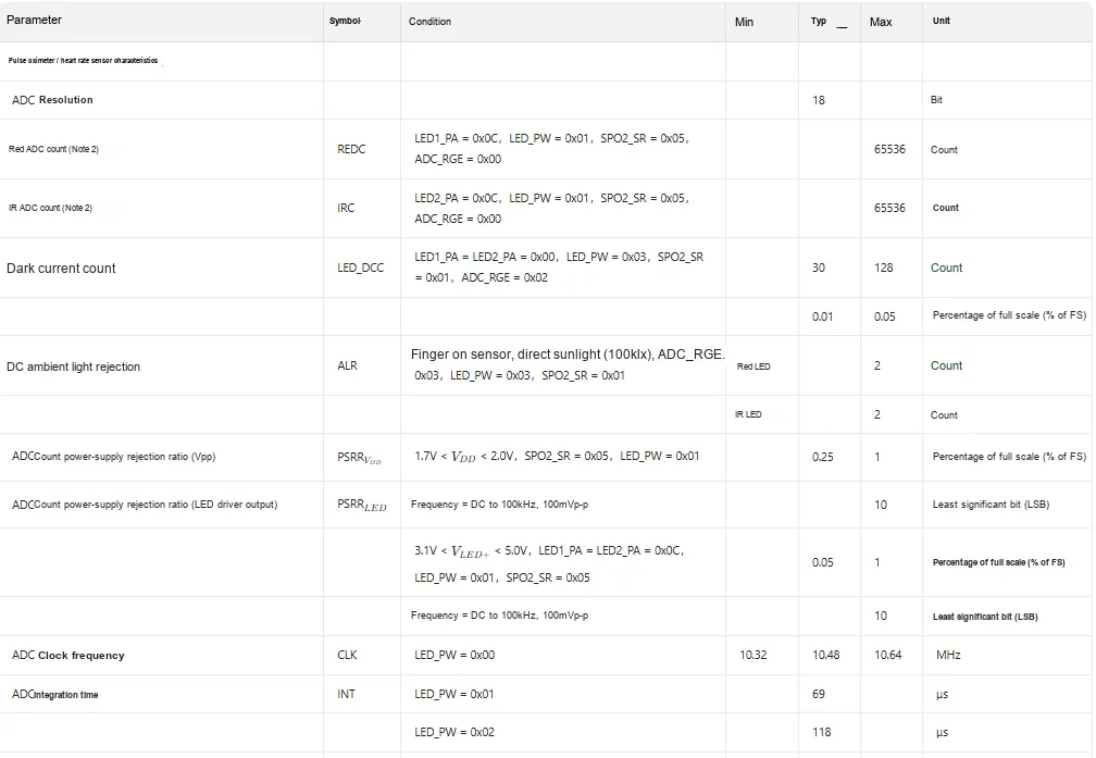
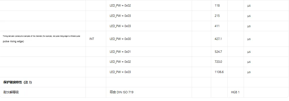
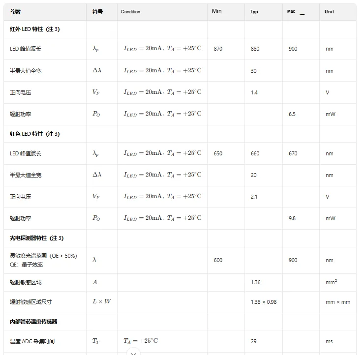
The following are the charts respectively illustrating the electrical characteristics, pulse oximeter/heart rate sensor characteristics, red LED characteristics, photodetector and temperature sensor characteristics of MAX30102EFD+ T.
MAX30102EFD+ T Key points are specified as follows:
- Temperature Sensor: Accuracy ±1℃(TA=+ 25∘C), Range -40~85℃.
- Digital Input (SCL, SDA):
- Input high voltage 0.7VDD (VDD = 2V), low voltage 0.3VDD (VDD = 2V);
- Hysteresis voltage 0.2V;
- Input Leakage Current ±0.05 to ±1 μA (VIN = GND or VDD, static state).
- Digital Output (SDA, INT): Output low voltage 0.2V (ISINK= 6mA).
- Electrical Characteristics (Power Supply):
- Supply Voltage VDD: 1.7~2.0V
- LED Power Supply Voltage VLED+: 3.1~5.0V;
- Power supply current: 600~1200μA during operation, 0.7~10μA when shut down.
- Pulse Oximeter / Heart Rate Sensor:
- ADC resolution: 18 bits;
- Maximum count for red and infrared ADC is 65536;
- Dark current count: 30~128;
- Under DC ambient light, the suppression on both red and infrared LEDs is ≤2 counts;
- The ADC has corresponding performance indicators such as power supply rejection ratio;
- ADC clock frequency: 10.32~10.64MHz, integration time: 69~118μs.
- LED and Photodetectors:
- Peak wavelength of infrared LED: 870~900nm, forward voltage: 1.4V, radiant power: ≤6.5mW;
- Peak wavelength of red LED: 650~670nm, forward voltage: 2.1V, radiant power ≤ 9.8mW;
- Sensitivity range of the photodetector: 600~900nm, with a sensitive area of 1.36mm²;
- Temperature ADC acquisition time 29ms (TA = + 25∘C).
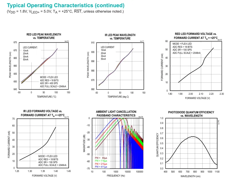
The operating characteristics of the MAX30102EFD+ T (heart rate / blood oxygen sensor) are described as follows:
- LED Peak Wavelength vs. Temperature Characteristics (Top Left / Top Middle): The peak wavelength of red/IR LEDs increases as temperature rises. This trend remains consistent across different LED operating currents (10mA to 50mA), reflecting the influence of temperature on the emission wavelength band.
- LED Forward Voltage-Current Characteristics (Top Right / Middle Left): At 25°C, the forward current of red/IR LED increases as the forward voltage rises, which matches the driving characteristics under operating modes such as its FLEX LED.
- Ambient Light Rejection Passband Characteristics (middle-right): Under different pulse widths (PW), the ambient light rejection circuit exhibits more significant suppression effect on high-frequency signals (e. g., above 10kHz), which can reduce the interference of ambient light on heart rate / SpO2 detection.
- Quantum Efficiency of Photodiode (bottom right): The photodiode exhibits a relatively high quantum efficiency within the wavelength range of 600~800 nm (corresponding to the emission band of red/IR LEDs), which adapts to the requirements of optical signal reception for the sensor and ensures detection accuracy.
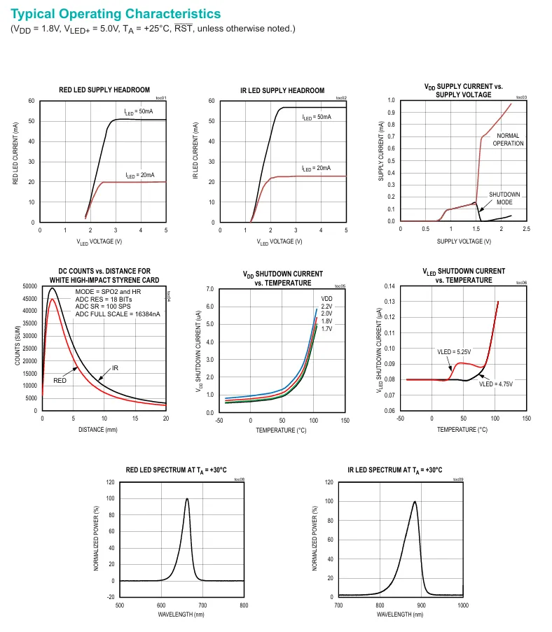
This set of diagrams demonstrates the typical operating characteristics of the MAX30102EFD+ T (heart rate / blood oxygen sensor):
- LED Current Characteristics (Top Left / Top Middle): The current of red / IR LEDs varies with the supply margin (Vf voltage difference), and stabilizes at a typical value (e. g., 50mA, 200mA) once a certain margin is reached;
- Supply Current Characteristics (top right): The VDD supply current is extremely low in shutdown mode, and increases with the rise of supply voltage in normal operation mode;
- Relationship between distance and detection value (left and middle): When detecting a white styrene card, the DC count value of the red/IR LED decreases as the detection distance increases, reflecting its ranging/signal attenuation characteristics;
- Shutdown Current vs. Temperature (Middle-right / Lower-middle): The shutdown currents of VDD and VLED increase with rising temperature, and the variation trend remains consistent across different supply voltages;
- LED Spectra (bottom left / bottom right): At 30°C, the peak wavelength of the red LED is approximately 660 nm, and that of the IR LED is around 880 nm, which correspond to the typical emission bands for heart rate / blood oxygen detection.
2.5 Reference Circuit
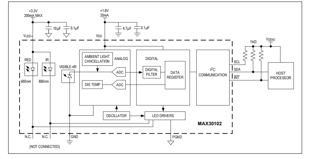
This is the functional block diagram of MAX30102: it is powered by dual power supplies (VLED+ is 3.3V, Vdd is 1.8V, both equipped with filter capacitors), and has built-in RED (660nm), IR (880nm) and other LEDs and photosensitive elements. After filtering out interference through the "ambient light cancellation module", the optical signal and chip temperature signal are converted into digital quantities via ADC respectively, and then stored in the data register after digital filtering;The oscillator cooperates with LED drive control to LED operate, and finally communicates with the host processor via the I2C interface; the INT pin transmits interrupt signals, which is mainly used for detecting physiological parameters such as heart rate and blood oxygen.
2.6 Chip Configuration
MAX30102EFD+ T is a heart rate and blood oxygen sensor that requires no additional configuration during use.
2.7 Communication Interfaces and Related Protocols
2.7.1 Register Description
2.7.1.1 Register Address Summary Table
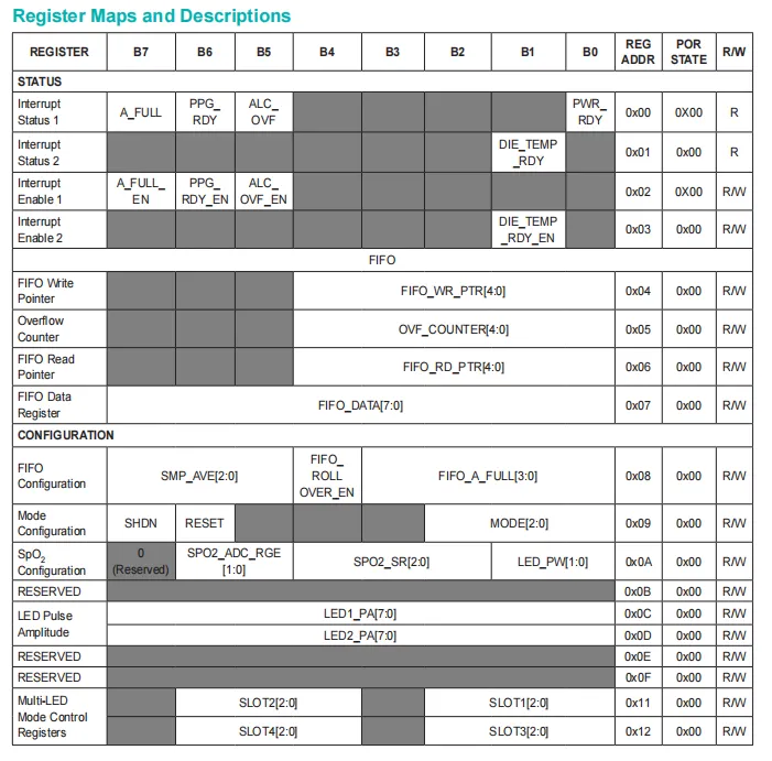
2.7.1.2 Interrupt
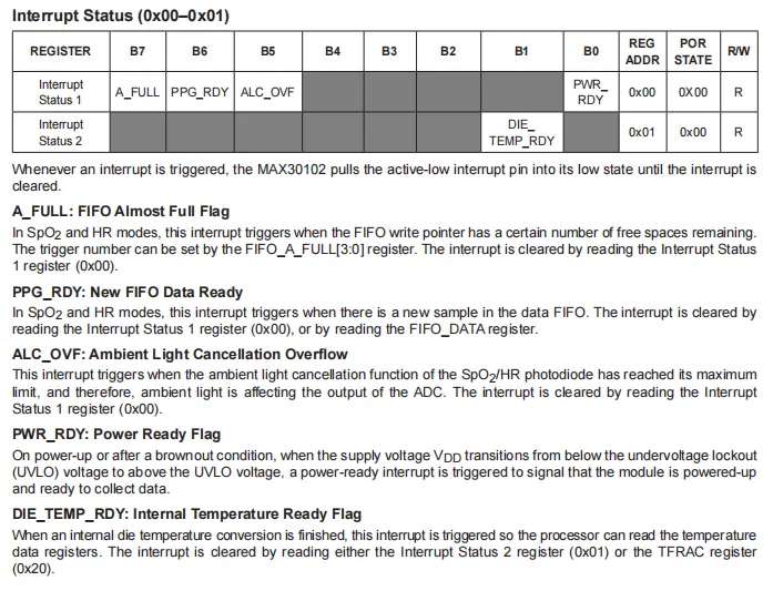
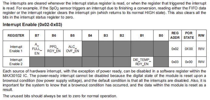
MAX30102 generates interrupts via the active-low INT pin; the interrupt status is recorded by 2 read-only interrupt status registers (0x00, 0x01), and controlled by 2 read-write interrupt enable registers (0x02, 0x03): except for the PWR_RDY (power ready) interrupt which cannot be disabled, the following 4 interrupts — A_FULL (FIFO almost full), PPG_RDY (new FIFO data available), ALC_OVF (ambient light cancellation overflow), and DIE_TEMP_RDY (internal die temperature ready)— can be enabled or disabled via the enable registers, and all of these interrupts are disabled by default.
Interrupt trigger scenarios vary as follows: A_FULL corresponds to the remaining space of the FIFO reaching the set value, PPG_RDY corresponds to new data being written into the FIFO, ALC_OVF corresponds to the ambient light cancellation function exceeding the limit, PWR_RDY corresponds to being ready after power-on/power-off recovery, DIE_TEMP_RDY corresponds to the completion of internal temperature conversion;After an interrupt is triggered, reading the corresponding status register or the register that triggered the interrupt (e. g., PPG_RDY to read FIFO_DATA) will clear the interrupt, INT pin returns to high level, and the corresponding bit in the status register will also be cleared to zero.
2.7.1.3 FIFO
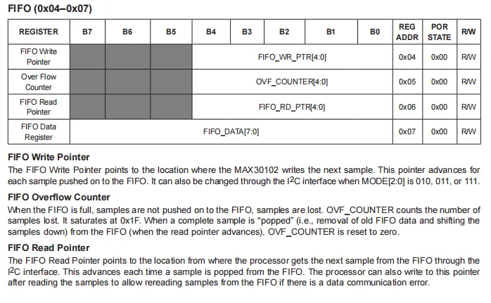
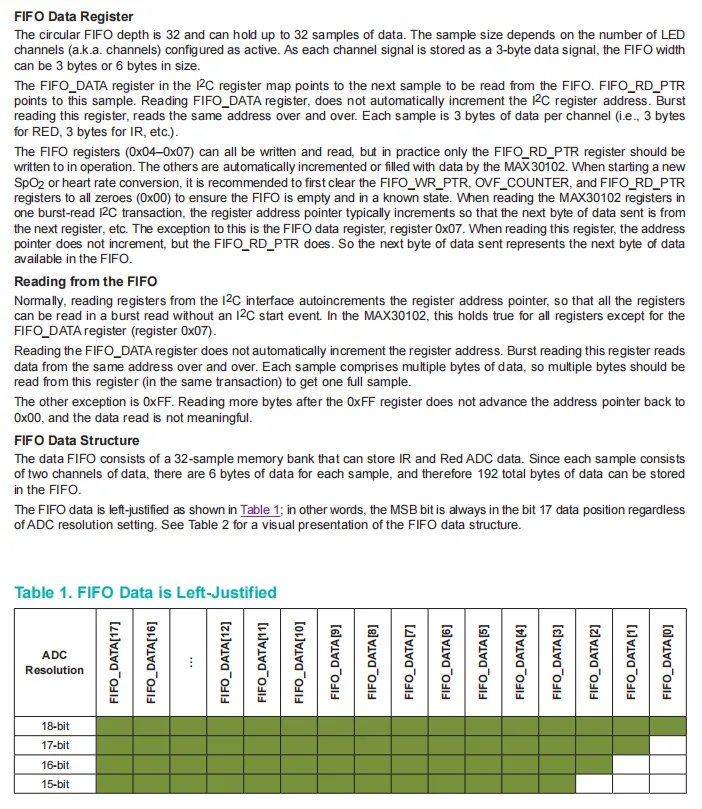
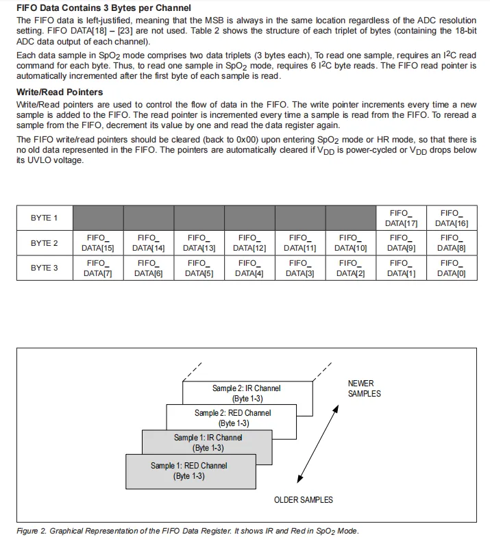
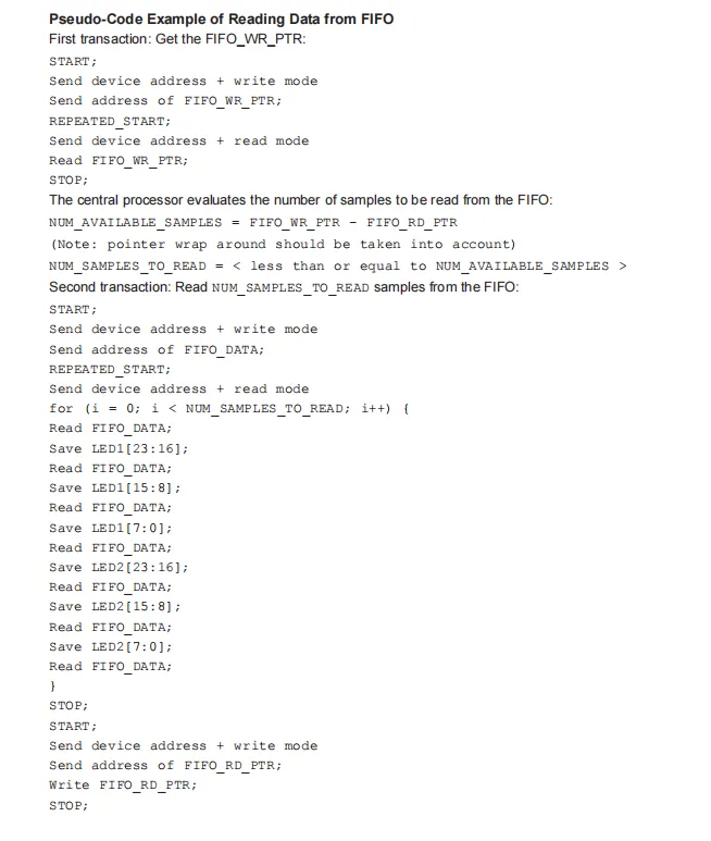
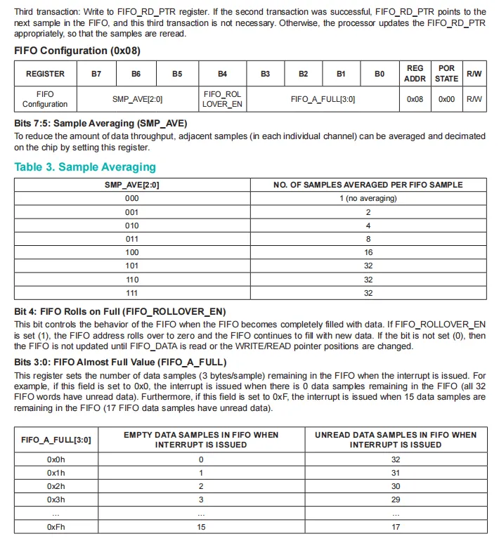
MAX30102 's FIFO is a circular buffer with a capacity of 32 samples, managed by the write pointer (FIFO_WR_PTR), read pointer (FIFO_RD_PTR), overflow counter (OVF_COUNTER) and data register (FIFO_DATA)(corresponding to registers 0x04 to 0x07): the write pointer points to the position to be written and increments with each stored sample; the read pointer points to the position to be read and increments with each read sample; the overflow counter counts the number of samples lost when the FIFO is full (and is cleared after a sample is read).
Its data is stored in left-aligned format, and each channel (e. g., RED / IR) sample occupies 3 bytes; in blood oxygen mode, one sample contains 2 channels totaling 6 bytes; when reading FIFO_DATA, the address pointer does not automatically increment, and multiple bytes need to be read consecutively to obtain a complete sample.
FIFO can be configured via the 0x08 register: SMP_AVE sets the averaging of 1-32 merged samples, FIFO_ROLL_OVER_EN controls whether to overwrite old data when the FIFO is full, and FIFO_A_FULL configures the remaining sample count for the almost-full interrupt; it is recommended to clear the pointer before entering the SpO2/heart rate mode to avoid interference from old data.
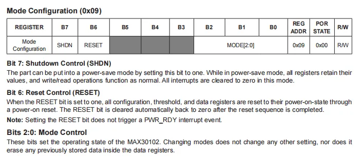
2.7.1.4 Mode Setting (0x09)
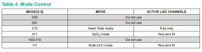
MAX30102 operating mode is configured via the Mode Configuration register (0x09) through its MODE[2:0] bits. The primary valid modes are as follows: 010 corresponds to heart rate mode (only the Red LED is activated), 011 corresponds to blood oxygen (SpO₂) mode (both Red and IR LED are activated), 111 corresponds to multi- LED mode (also activates both Red and IR LED); other mode combinations (such as 000,001, etc.) are not recommended.Different modes adapt to the acquisition requirements of different physiological parameters such as heart rate and blood oxygen by switching the activated LED channels.
2.7.1.5 Blood Oxygen Saturation Setting (0x0A)
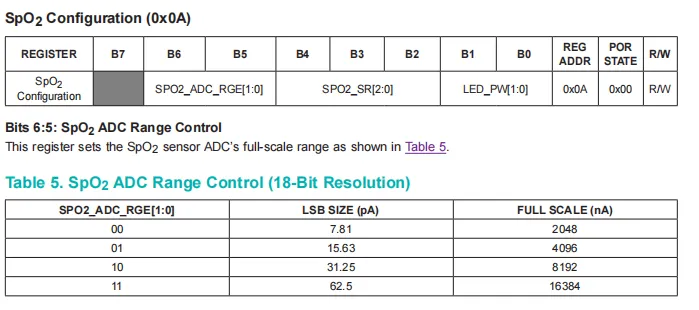
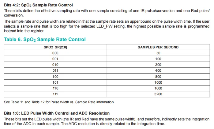
MAX30102 's SpO₂ configuration register (0x0A) is used to set the core acquisition parameters in the blood oxygen mode, which consists of three key configuration segments:
SPO₂_ADC_RANGE(Bits 6-5): Controls the full-scale range of theADC, with selectable ranges such as 2048 nA to 16384 nA. These ranges correspond to differentLSBaccuracies, adapting to optical signal acquisition of varying intensities;SPO₂_SR(Bits4-2): Set the sampling rate (50~3200 samples/sec), which must match the pulse width ofLED; an excessively high setting will be automatically adjusted to the maximum feasible value;LED_PM(Bits 1-0): Controls the pulse width ofLED(infrared, red light), and indirectly determines the integration time and resolution of theADC.
These configurations collectively adapt to the requirements such as signal accuracy and rate for blood oxygen acquisition.
2.7.1.6 LED Pulse Amplitude (0x0C-0X0D)
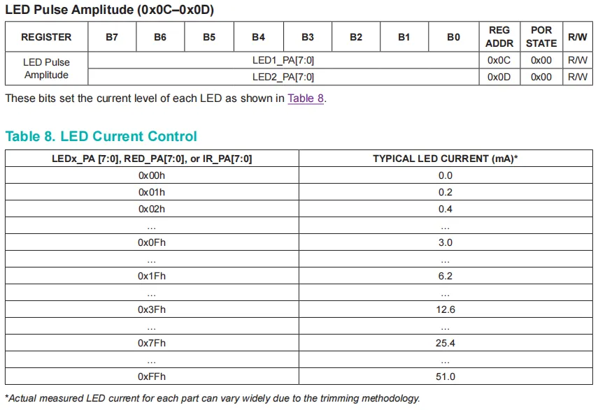
This part of the function is MAX30102 to configure the operating parameters of the LED, which consists of two core modules:
- LED pulse width control: The pulse width (69μs~411μs) of
LED(red light, infrared light) is set via bits [1:0] ofLED_PM, which also directly determines the resolution (15~18 bits) ofADC— the longer the pulse width, the longer the integration time ofADC, the higher the resolution, and the better the acquisition accuracy. - LED Pulse Amplitude Control: The
0x0Cand0x0Dregisters'LEDx_PA[7:0] bits respectively adjust the currents of the red and infraredLEDs(ranging from 0.0mA to 51.0mA), so as to control the luminous intensity of theLEDsand adapt to the optical signal requirements of different detection scenarios (such as different skin tones and wearing tightness; the actual current may vary slightly due to device calibration).
These two configurations jointly optimize the emission parameters of the LED, and coordinate with the precision and adaptability of subsequent signal acquisition.
2.7.1.7 Multi-LED Mode Control Registers (0x11–0x12)
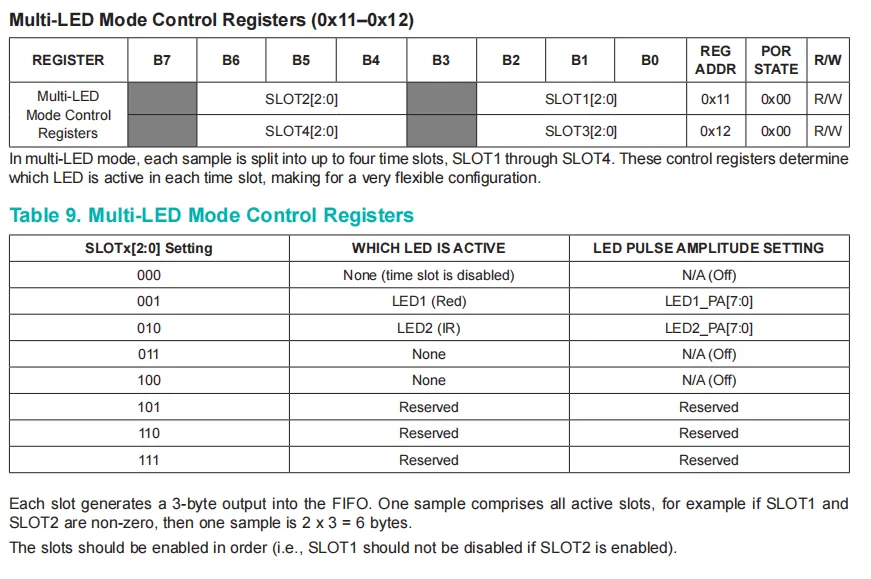
This part describes the multi- MAX30102 - LED mode control function, which is managed by registers 0x11 and 0x12: In multi- LED mode, each sample is split into up to 4 time slots (SLOT1 to SLOT4), and the LED to be activated in each slot can be configured via the SLOTx[2:0] bits of that slot (only 001 corresponds to red light LED1, 010 corresponds to infrared LED2, and the rest are mostly disabled/reserved); activated slots will call the corresponding LED pulse amplitude parameters (LED1_PA / LED2_PA).Each activation slot writes 3 bytes of data to the FIFO (if 2 slots are activated, one sample occupies 6 bytes), and the slots must be enabled in the order from SLOT1 to SLOT4; subsequent slots cannot be enabled without enabling the preceding slots.
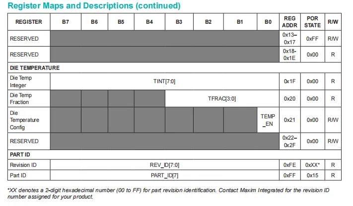
2.7.1.8 Temperature Data (0x1F–0x21)
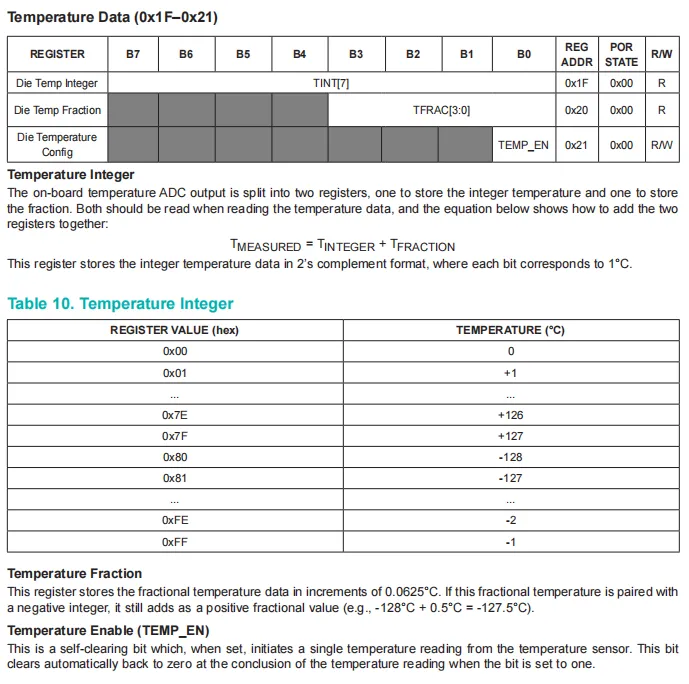
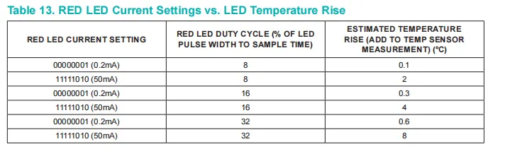
This part describes the on-board temperature detection and compensation function of MAX30102:
- Temperature Measurement: A single temperature reading is triggered via the
TEMP_ENbit of register 0x21 (this bit is automatically cleared after triggering). The measurement result is stored in two separate registers: 0x1F (integer part, in two's complement format, where 1 bit corresponds to 1°C) and 0x20 (fractional part, with an increment of 0.0625°C). The actual temperature is obtained by adding the values of the two registers (e. g., -128°C + 0.5°C = -127.5°C). - Temperature Compensation: Since
LEDheat generation will change the red light wavelength (which affects blood oxygen measurement), it is necessary to look up the table to obtain the temperature rise value of theLEDaccording to the current setting and duty cycle of theLED, add it to the temperature measured by the sensor to estimate the actual temperature of theLED, so as to improve the acquisition accuracy of parameters such as blood oxygen.
2.7.2 IIC Communication Description
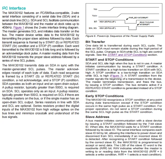
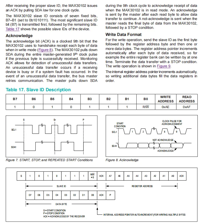
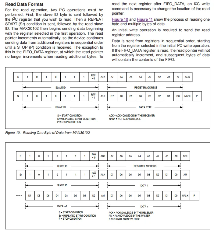
MAX30102 operates I2C communication in master-slave mode: its fixed 7-bit slave address is "1010111", corresponding to the write address 0xAE and read address 0xAF. The communication is initiated by the master sending a START condition (pulling SDA low while SCL is high) and terminated by a STOP condition (pulling SDA high while SCL is high), with acknowledgment via ACK / NACK at the 9th clock cycle after each byte transmission.
Write operation , the host sequentially sends a write address from the machine, the target register address ( ACK are obtained MAX30102 ), and then sends data bytes (back to ACK after each byte), the register pointer is automatically incremented, and finally STOP ends; read operation needs to send a write address to specify the register, and then send a repeat START and read address, MAX30102 after sending data response, the host intermediate byte back ACK , the last byte back to NACK , only read FIFO_DATA when the register pointer is not automatically incremented, in order to complete the data read and write interaction.
2.8 PCB Routing Precautions
None.
III. Circuit Engineering
3.1 Circuit Source Engineering
To obtain the source code of the circuit, please follow the official account [Freak Embedded]
3.2 Module Usage Instructions
SCH_Schematic1_Heart Rate and Blood Oxygen Sensor Module Based on MAX30102 Chip-V1.0_2025-11-13.pdf 2.1 MB
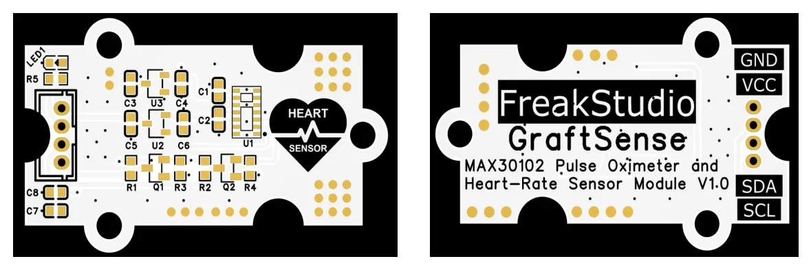
This module provides an I2C communication interface: it supports standard I2C communication rate, with the default configured slave address of 0x57 for I2C, is compatible with 3.3V system level to adapt to mainstream microcontrollers, can stably transmit the digital data of heart rate and blood oxygen corresponding to red light and infrared light detection, is applicable to scenarios such as health monitoring devices and wearable maker projects, and provides a convenient hardware connection solution for the digital collection of physiological parameters and system interaction.
3.3 Application Experiment
Here, we use the GraftPort-RP2040 development board for testing, and connect the heart rate and blood oxygen sensor module based on the MAX30102 chip to communicate with the main controller via the I2C interface.
Here, we first use the HY2.0-4P cable to connect the module to the GraftPort-RP2040 development board's I2C0 interface:
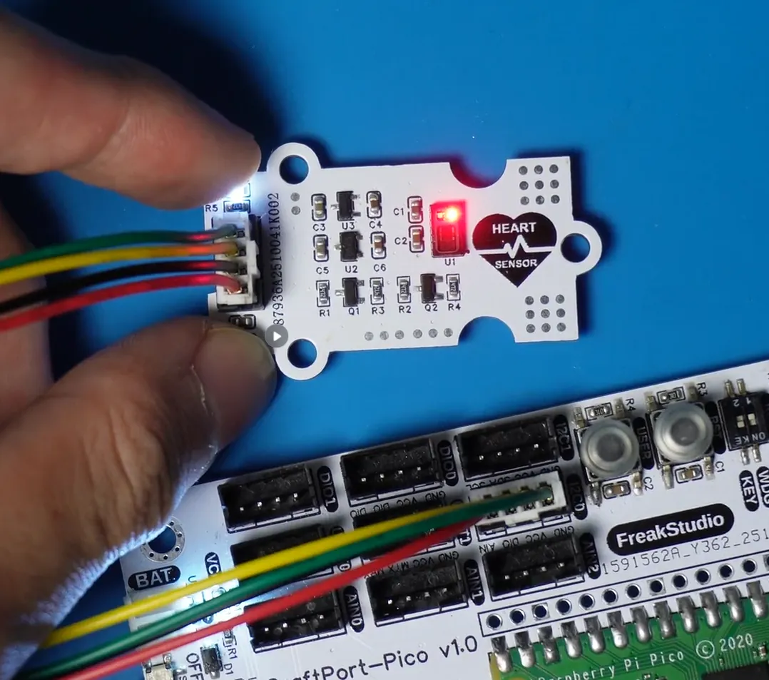
The module connections are shown in the following table:
Development Board Pins | Module Pins | Description |
Pin 4 |
|
|
Pin 5 |
|
|
Here, we need to search for relevant driver packages on uPyPI: https://upypi.net/zh/

Enter max30100_driver to search, and the following will be displayed:

Click to copy the local installation command:

Here, we can use the mip tool to import module driver library code. Below are the usage commands for the mpremote tool:
mpremote mip install github:FreakStudioCN/GraftSense-Drivers-MicroPython/sensors/max30102_driverAfter importing the heart rate and blood oxygen sensor module based on the MAX30102 chip - MicroPython driver code, copy the following main.py code into our project:
# Python env   : MicroPython v1.23.0
# -*- coding: utf-8 -*-
# @Time    : 2025/09/16 18:00
# @Author  : 侯钧瀚
# @File    : main.py
# @Description : MAX30102 heart rate and PPG reading + simple heart rate calculator example

# ======================================== Import Modules =========================================

# MicroPython built-in module
from machine import I2C, Pin
# Import time-related modules
import time
# Import the MAX30102 driver module
from heartratemonitor import MAX30102, MAX30105_PULSE_AMP_MEDIUM , HeartRateMonitor, CircularBuffer

# ======================================== Global Variables ============================================

# Calculate the heart rate every 2 seconds
hr_compute_interval = 2

# ======================================== Functions ============================================

# ======================================== Custom Classes ============================================

# ======================================== Initialization ==========================================
# Power-on delay of 3 s
time.sleep(3)
# Print debug message
print("FreakStudio: Use MAX30102 to read heart rate and temperature.")
# I2C0: SDA=GP4, SCL=GP5, 400kHz
i2c = I2C(0, sda=Pin(4), scl=Pin(5), freq=400000)
# Create the sensor instance
sensor = MAX30102(i2c=i2c)
# Basic initialization
sensor.setup_sensor()
# Sample rate: 400 Hz
sensor_sample_rate = 400
sensor.set_sample_rate(sensor_sample_rate)
# FIFO averaging: 8
sensor_fifo_average = 8
sensor.set_fifo_average(sensor_fifo_average)
# LED current: medium
sensor.set_active_leds_amplitude(MAX30105_PULSE_AMP_MEDIUM)
# Expected acquisition rate: 400 / 8 = 50 Hz
actual_acquisition_rate = int(sensor_sample_rate / sensor_fifo_average)  # Actual output Hz
# Initialize the heart rate monitor
hr_monitor = HeartRateMonitor(
        # Sample rate matches the sensor
        sample_rate=actual_acquisition_rate,
        # Heart rate calculation window (about 2–5 s, 3 s is used here)
        window_size=int(actual_acquisition_rate * 3),
    )
# Reference time
ref_time = time.ticks_ms()

# ========================================  Main Program  ===========================================

while True:
        # Poll the FIFO for new data; if any, write it to internal storage
        sensor.check()
        time.sleep(0.5)
        # Whether the buffer has available samples
        if sensor.available():
            # Read RED/IR/TEMP channel data (integers)
            red_reading = sensor.pop_red_from_storage()
            ir_reading = sensor.pop_ir_from_storage()
            temp_reading =sensor.read_temperature()
            print("RED: {}, IR: {},TEMP:{:.2f}".format(red_reading, ir_reading,temp_reading))
            # Use IR samples for heart rate calculation (RED/IR/GREEN can be used depending on skin tone)
            hr_monitor.add_sample(ir_reading)


        # Calculate heart rate once every hr_compute_interval seconds
        if time.ticks_diff(time.ticks_ms(), ref_time) / 1000 > hr_compute_interval:
            heart_rate = hr_monitor.calculate_heart_rate()
            if heart_rate is not None:
                print("Heart Rate: {:.0f} BPM".format(heart_rate))
            else:
                print("Not enough data to calculate heart rate")
            # Reset reference time
            ref_time = time.ticks_ms()
Burn the code, open the terminal, and use the mpremote tool to connect to the main controller. Place your finger on the sensor, and the output will be as follows:
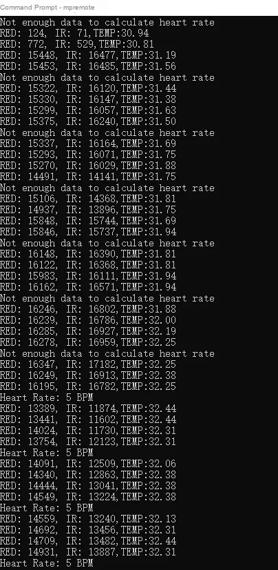
It can be seen that the routine can currently run normally and output RED, IR, TEMP, and the heart rate value will be output after sufficient data is collected.
Please note the following points when using it:
- Attach the sensor to the skin (fingertip pad, earlobe and other areas are recommended) to avoid gaps or hair blocking the optical window; do not cover the sensor with your fingernail (fingernails are opaque and will block light transmission), and keep the skin at the attachment site as flat as possible during wearing.
- Avoid direct exposure of the sensor to strong light (sunlight, intense artificial lighting), as ambient light will interfere with the optical signal; remain stationary during measurement, as movement or shaking will cause fluctuations in light intensity data and lead to distorted heart rate/blood oxygen calculations.
- This module features consumer-grade accuracy and cannot be used as a basis for medical diagnosis;Keep the optical window of the sensor clean (stains/fingerprints will block light) and wipe it gently after prolonged use.
IV. Drivers
max30102_driver.zip 25 KB
5. BOM & Recommended Alternative Parts
None.
VI. Revision History
Document Version | Date of Revision | Modifier | Revised Content |
v1.0 | 2025-11-13 | Zero Kōkō | Initialize the document |
v1.1 | 2025-12-29 | Li Zisheng | Added application experiments and production files |
v1.2 | 2025-12-31 | Xin Ruili | Create an open version of the document based on the internal document version v1.1. |
v1.3 | 2026-03-29 | Xin Ruili | Modified the application experiment section |
VII. Relevant Materials
7.1 Chip Datasheet
MAX30102 Manual.pdf 896 KB
7.2 Unique Icons for PCB Silk Screen