Contents
- I. Module Introduction
- II. Introduction to Main Chips
- 2.1 Chip Overview
- 2.2 Pin Definition
- 2.3 Functional Block Diagram
- 2.4 Performance Parameters
- 2.5 Reference Circuit
- 2.6 Chip Configuration
- 2.7 Communication Interfaces and Related Protocols
- 2.8 PCB Routing Precautions
- III. Instructions for Circuit Engineering and Module Usage
- 3.1 Circuit Source Engineering
- 3.2 Module Usage Instructions
- 3.3 Application Experiment
- IV. Drivers
- 5. BOM & Recommended Alternative Parts
- VI. Revision History
- VII. Relevant Materials
- 7.1 Chip Datasheet
- 7.2 Unique Icons for PCB Silk Screen
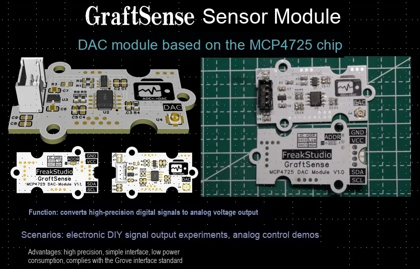
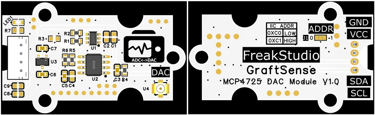
I. Module Introduction
Digital-to-Analog Conversion Module Based on MCP4725 Chip Based on MCP4725 chip, this module integrates a 12-bit high-precision digital-to-analog conversion function and adopts the I2C Communication Protocol, supporting standard, fast and high-speed multi-rate modes. The module has built-in DC-DC 5V to 3.3V circuit, voltage follower, etc. , which can work stably with a 5V power supply input, and can realize accurate conversion from digital signals to analog voltages. It also supports custom communication addresses, and is suitable for scenarios such as maker education, electronic prototype development, and industrial control, providing developers with a convenient single-channel digital-to-analog conversion solution.
II. Introduction to Main Chips
MCP4725 is Microchip a single-channel 12-bit digital-to-analog converter (DAC) manufactured by the company, featuring non-volatile EEPROM storage function. It is widely used in applications requiring precise analog signal output, such as audio signal generation, sensor signal conditioning and voltage reference adjustment.
2.1 Chip Overview
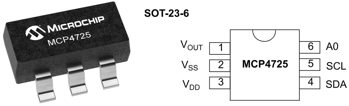
MCP4725 has the following key features:
- 12-bit resolution:
MCP4725offers 12-bit resolution, which means it can output 4096 distinct voltage levels, making it suitable for scenarios requiring high-precision signal generation. - I²C Interface:
The MCP4725communicates via theI2Cbus, which means it can be easily integrated with master devices such as microcontrollers, and the output of theI2CCommunication Protocol can be used to control theDAC - EEPROM Storage: This device has a built-in non-volatile
EEPROMthat can store the value of theDACoutput register, which means that the output value remains unchanged even when the device is powered off or restarted - Output Voltage Range:
The MCP4725has an output voltage range from 0 V toVcc, and the accuracy of the output voltage depends on the reference voltageVref, which is typically the same as the supply voltage - Low Power Consumption:
MCP4725is a low-power device, making it ideal for battery-powered applications - Compact package: It typically adopts
SOT-23orMSOP-8packages, which are ideal for space-constrained designs
2.2 Pin Definition
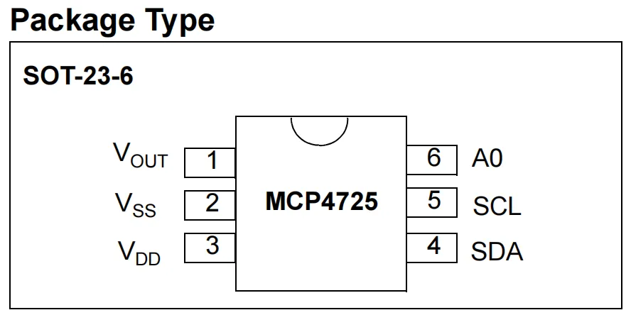
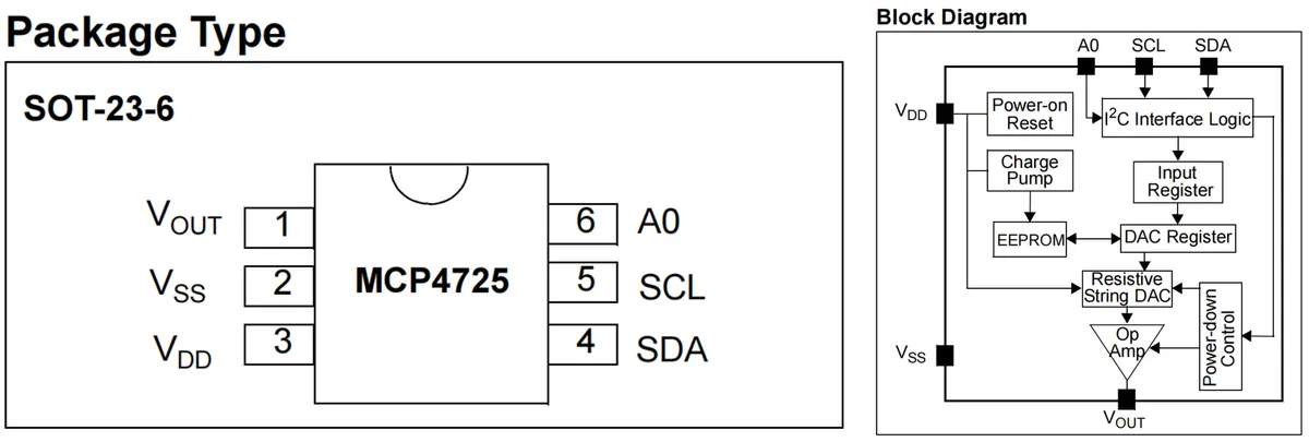
MCP4725 Pin functions are described as follows:
Pin Name | Description |
VOUT | Analog output voltage: the output terminal of the DAC, which is used to output the converted analog voltage signal, with an output voltage range between GND and VDD. |
VSS | Ground Reference: The ground pin of the DAC, which provides the ground reference for the circuit and is connected to the analog ground of the circuit board. |
VDD | Supply Voltage: This is the power supply pin of the DAC, which provides the required operating voltage; its input range is 2.7V to 5.5V, and a bypass capacitor is required for filtering. |
SDA | I2C Serial Data: Used for data transmission via the I2C interface. |
SCL | I2C Serial Clock Input: A data synchronization clock signal for the I2C interface. |
A0 | I2C Address Bit Selection Pin: This pin is used to select the I2C address bit of the DAC. It can be connected to VSS (ground) or VDD (power supply), or driven by a digital logic signal; the logic state of the A0 pin determines the I2C address. |
2.3 Functional Block Diagram
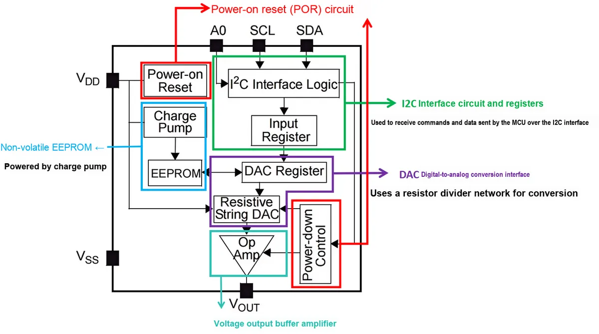
2.4 Performance Parameters
The following introduces the electrical parameters of the MCP4725:
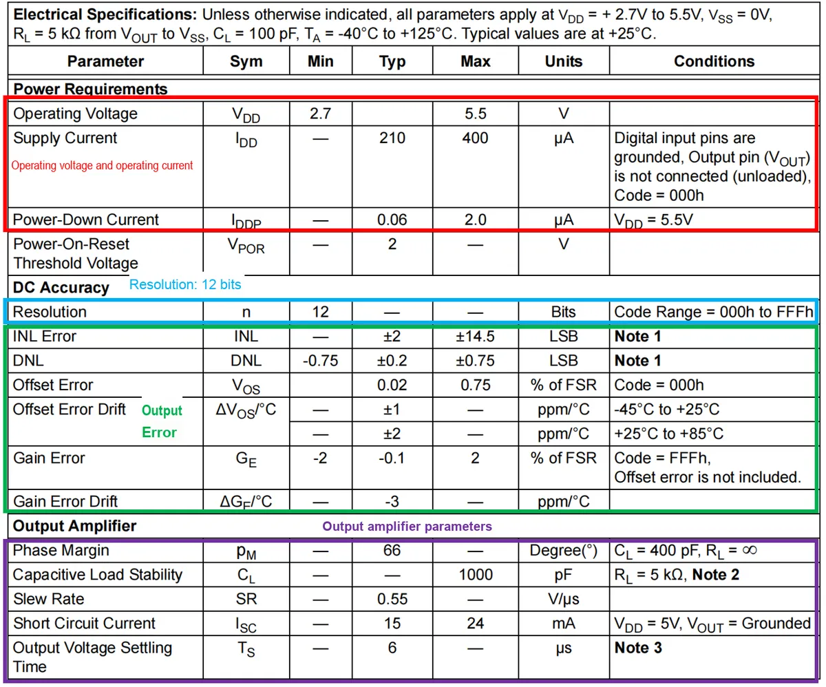
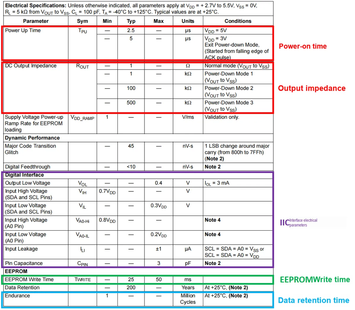
The key parameters are as follows:
- Operating Voltage (
VDD) : The supply voltage range in which theDACcan work normally, 2.7V to 5.5V. - Supply Current (
IDD):DACcurrent consumption in normal operation mode, with a typical value of 210 µA. - Power-Down Current (
IDDP):DACcurrent consumption when entering power-down mode, with a typical value of 0.06 µA. - Integral Non-Linearity Error (
INL) : The error between theDACoutput and the ideal linear output, with a maximum value of ± 14.5LSB, represents the linearity of theDACoutput; if theINLerror is large, the deviation between theDACoutput and the expected value will increase. - Differential Non-Linearity Error (
DNL): the error between the analog outputs corresponding to two adjacent digital values, with a typical value of ±0.2LSB; a smallerDNLindicates that the output variation of aDACbetween different digital values is more uniform. - Gain Error (
GE) : The error between the actual gain of theDACoutput voltage and the ideal gain, typically -0.1% (maximum 2%), a large gain error may cause the output voltage to deviate from the expected value. - Output Voltage Settling Time (
TS) : The time it takes for theDACoutput voltage to stabilize from one value to another, typically 6 µs. A shorter settling time indicates that theDACcan respond quickly to input changes. - Power-up time:
DACThe time from power-on to full readiness; a shorter power-up time means the device can start operating normally faster, which is particularly important in applications requiring frequent restarts - Resistive Output Impedance (
ROUT):DACoutput internal resistance. The low output impedance (1 Ω) in normal mode helps stabilize the output voltage, while the high impedance value in power-saving mode affects the load capacity of theDACoutput. EEPROMwrite time: the time required to write toEEPROM.- Data retention time:
EEPROMthe duration for which data can be retained without power supply.
2.5 Reference Circuit
2.5.1 Simple Voltage Output of MCP4725
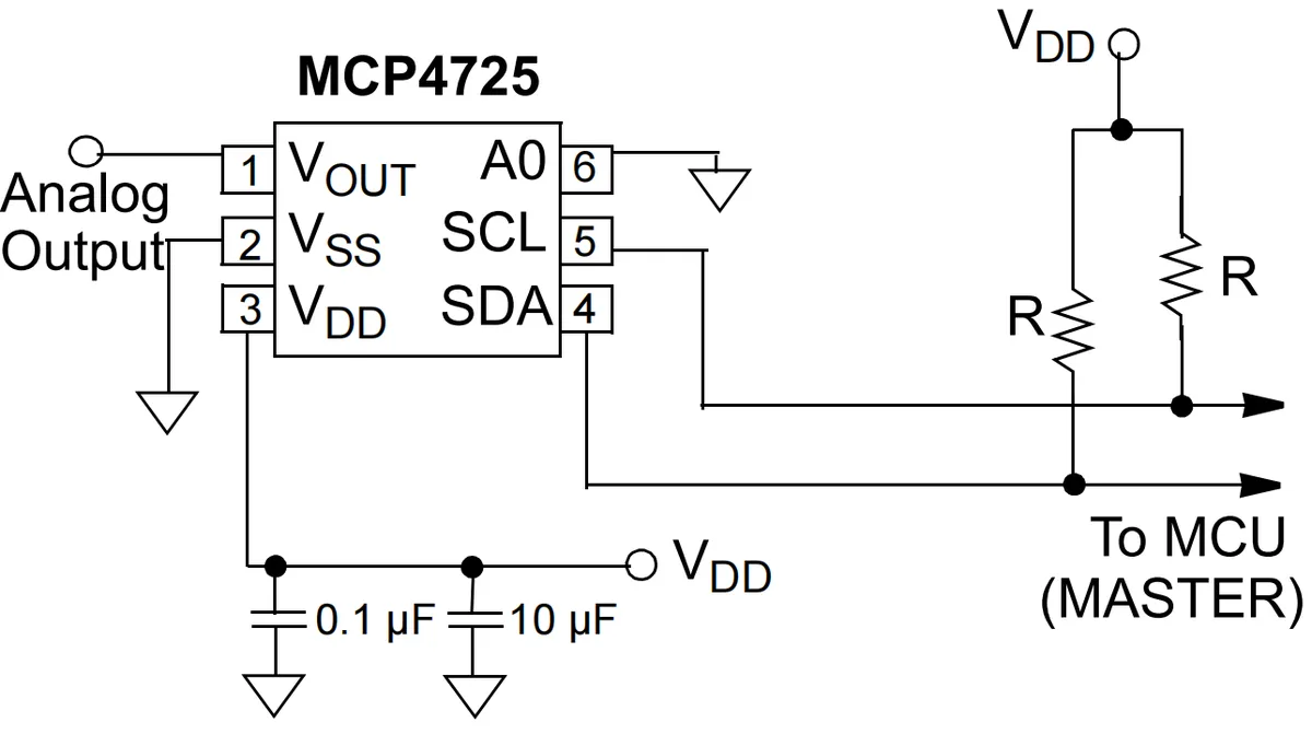
At this point, Vout serves as the analog voltage output, the A0 pin can be connected to GND, VDD or a digital pin of the microcontroller to set the I2C address, and two pull-up resistors, typically ranging from 1kΩ to 10kΩ, are connected to the I2C communication interface.
VDD input voltage is typically connected to two filtering capacitors, commonly a 10µF tantalum capacitor and a 0.1µF ceramic capacitor; meanwhile, during PCB layout routing, these capacitors should be placed as close as possible to the VDD pins (within a distance of 4 mm).
MCP4725 The schematic diagram of the simple voltage output is as follows:
2.5.2 MCP4725 Reduce Output Step Size
When VDD is 3.3 V, the MCP4725 has an output voltage step size of 3.3 V / 4096 ≈ 0.805 mV. Some applications may require an extremely small DAC output voltage step (e. g., 200 µV), which can be achieved by using a voltage divider at the DAC output. The voltage divider scales down the output step of the DAC while mitigating the impact of noise.
The following circuit is designed for accurate detection of optical sensor signals and fine adjustment of output voltage, and it is used to detect whether the light intensity reaches the preset threshold:
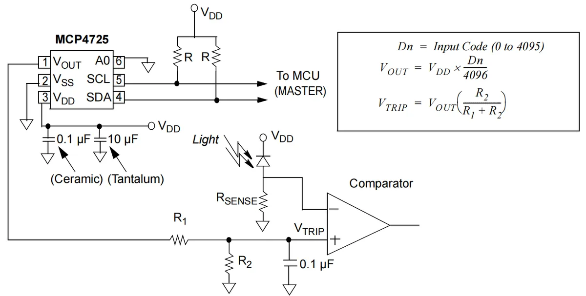
Wherein, R1 and R2 form a voltage divider, which is configured to adjust the output voltage DAC of VOUT to a smaller voltage VTRIP, and the calculation formula for VTRIP is as follows:
The other end of the comparator is connected to the sensing resistor (RSENSE) and the photodiode; this resistor is used to sense the current flowing through the photodiode. Under illumination, the photodiode generates a current, which creates a voltage drop across RSENSE; the comparator is used to determine the voltage difference between VTRIP and the voltage across RSENSE, thereby generating a corresponding output signal. The comparator can be used to detect the light intensity or whether the current exceeds a set threshold.
2.5.3 MCP4725 Builds a "Window" DAC
For sensor applications that require extremely high resolution around a setpoint or threshold voltage, a "window" can be constructed by using a voltage divider network with pull-up and pull-down resistors DAC, which can significantly improve the step resolution while narrowing the output voltage range.
The following circuit is used to detect whether the current in the circuit exceeds the safe range:
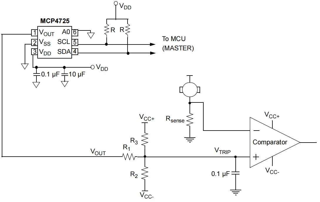
Wherein, MCP4725 generates an analog voltage Dn based on the input digital code, and the resulting analog voltage VOUT is given by:
R1, R2, R3 form a voltage divider circuit that converts VOUT into the comparator input voltage VTRIP. For ease of analysis, the circuit can be simplified to a Thevenin equivalent circuit, and the calculation formulas for its equivalent resistance and voltage are as follows:
The voltage finally input to the comparator VTRIP is:
Current sensing resistor Rsense is used to measure the current flowing through the load. It compares the voltage drop caused by the current with VTRIP to determine whether the current has reached the set threshold.
2.5.4 Bipolar Voltage Output of MCP4725
Bipolar operation of the MCP4725 can be achieved by using an external operational amplifier. This configuration allows users to achieve almost any desired output voltage range, power and noise performance by selecting appropriate resistance values. The gain of the op-amp is determined by the resistors R1 and R2, while R3 and R4 are used to adjust the output offset of the DAC.
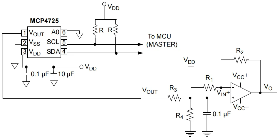
Wherein, the operational amplifier circuit is configured to buffer and amplify MCP4725 the output signal;R1 and R2 form an adjustable gain circuit that allows users to select an appropriate gain, while R3 and R4 are configured to shift the output voltage of DAC to the required bias level.
If a higher bias voltage is required, R4 can be connected to VDD instead of VSS, while a pull-up resistor is used to replace R4.
2.5.5 Current Output of MCP4725
By adding a voltage follower and a sensor resistor, the voltage output by DAC can be converted into a digitally controlled current source. This type of circuit is commonly used to drive LEDs, lasers, or other loads that require a stable current supply. By programming the voltage output by DAC, the current flowing through the load can be precisely controlled.
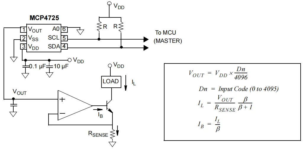
Among them, the operational amplifier supplies different base currents to the triode under different voltages, thereby adjusting the current flowing through the load; by measuring Rsense, the operational amplifier adjusts its output to ensure that the current remains constant.
2.6 Chip Configuration
2.6.1 Chip Address Selection
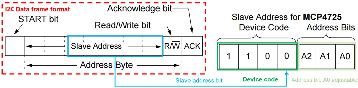
The MCP4725 I2C device address consists of four fixed bits (1100 = device code) and three address bits (A2, A1, A0). Among these, the A2 and A1 bits are hardwired during the manufacturing process and programmed to "00" by default, while the A0 bit is determined by the logic state of the A0 pin.
The A0 pin can be connected to VDD or VSS, or be driven by a digital logic level, as shown in the following figure:
2.6.2 Operating Modes of MCP4725
The device has two operating modes: normal mode and power-saving mode. The mode is selected by programming the power-down bits (PD1 and PD0) in the configuration register, and users can also program these two power-down bits in non-volatile EEPROM storage.
- Normal Mode: The device performs normal digital-to-analog conversion
- Power-down mode / Power-saving mode: The device enters a power-saving state, with most internal circuits turned off; in power-saving mode, all internal circuits (except the
I2Cinterface) are disabled, no data conversion events occur, and there is noVOUToutput. The output stage switches to a known resistive load, the value of which is determined by the state of the power-down bit. Setting the power-saving mode can also avoid unnecessary output voltages (e. g., during startup or shutdown).
The setting of the power-off bit is as follows:
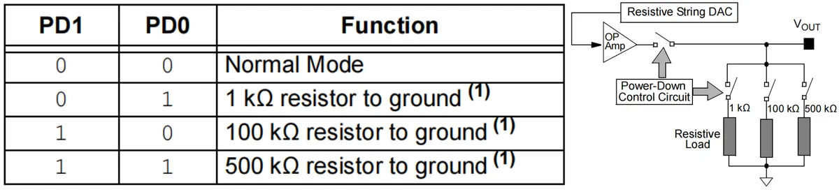
By selecting an appropriate pull-up resistance value, the leakage current at the output terminal in Power-Down mode can be controlled.
2.7 Communication Interfaces and Related Protocols
MCP4725 communicates with the master device (MCU) via the I2C bus and operates as a slave device; the master device can write to or read from the DAC input register or EEPROM through the I2C interface commands.
2.7.1 EEPROM Storage of MCP4725
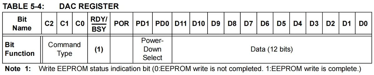
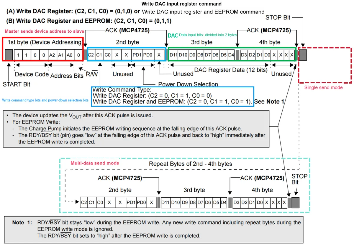
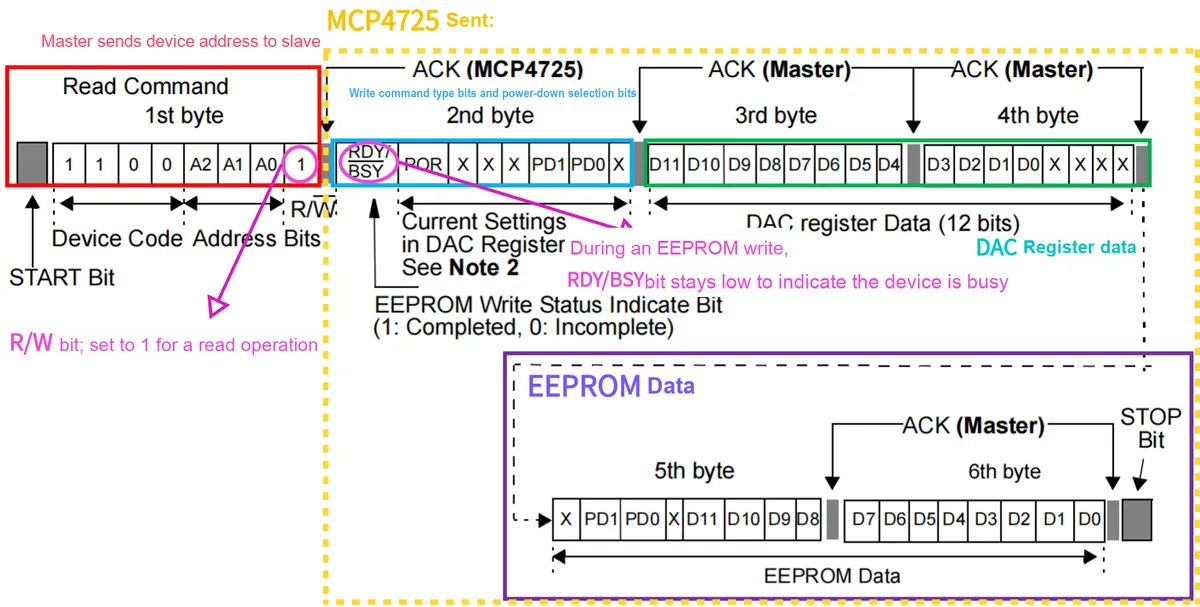
MCP4725 features a 14-bit wide EEPROM memory used to store configuration bits (2 bits) and DAC input data (12 bits). These bits can be read from and written to via commands over the I2C interface. An EEPROM write operation is initiated when an EEPROM write command is received (data bits C2 = 0, C1 = 1, C0 = 1). During the write operation, the status bit RDY / BSY remains low until the write operation is completed. Once the write operation finishes, the RDY / BSY data bit goes high.During the write period, any new write command will be ignored.
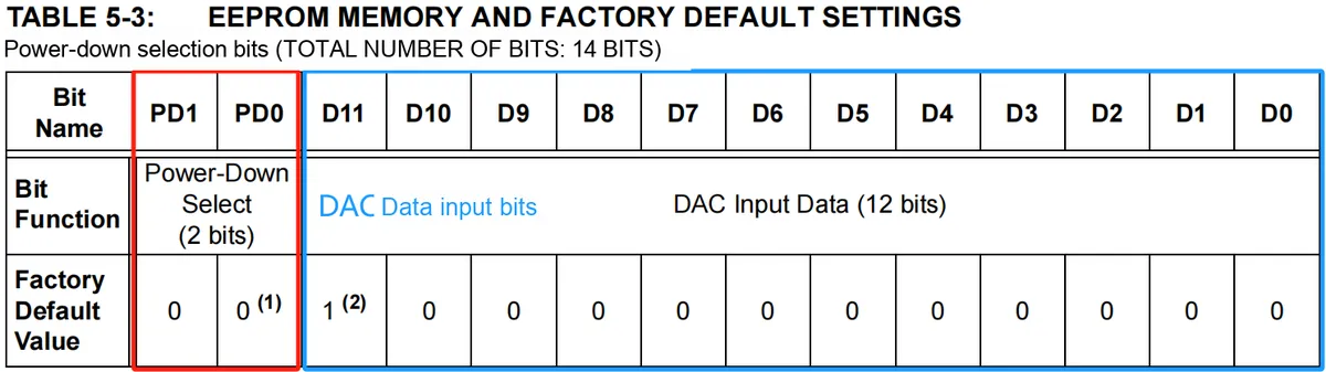
2.7.2 Operating Mode of MCP4725
2.7.2.1 Write Command of MCP4725
We can input the analog voltage code to be output through the I2C interface. The input code of MCP4725 is unsigned binary, and its output voltage ranges from 0 V to VDD. The calculation formula for the output voltage is as follows:
Wherein, D is the DAC input data (ranging from 0 to 4095).
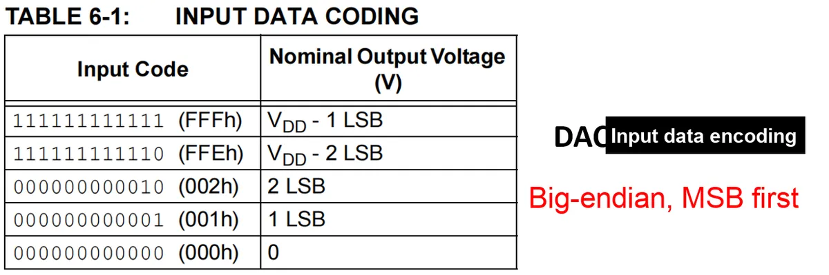
The write command is used to load configuration bits and DAC input codes into DAC registers, or to write to the device's EEPROM; the type of write command is defined by three write command type bits (C2, C1, C0).
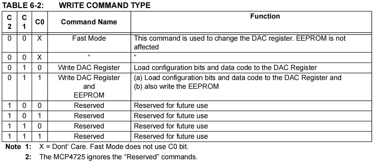
Among them, there are three types of write commands:
- Fast Mode Write Command (
C2= 0,C1= 0,C0= X): The fast write command is used to update theDACregisters; the device's EEPROM is not affected by this command. This command updates the power-down mode selection bits (PD1andPD0) and the 12-bitDACinput code in theDACregister. The device updatesVOUTon the falling edge of theACKpulse of the third byte:- We can send a stop bit to terminate the transmission after sending the three-byte command for the first time, thus completing one data transmission.
- It is also possible to send a repeated start bit after transmitting the 3-byte command for the first time, and then send new DAC input bytes (the second and third bytes) and power-down selection data bits, so as to implement multiple consecutive update operations.
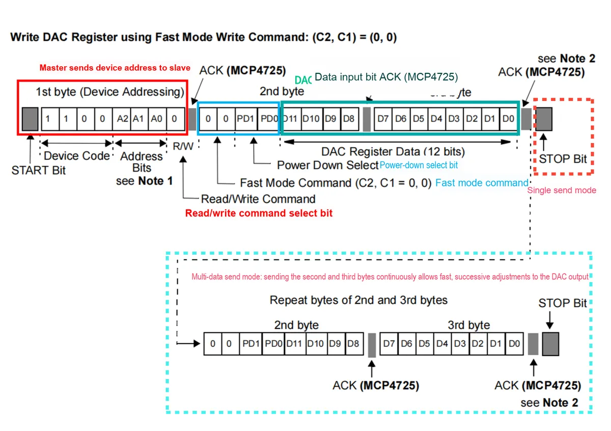
- Write
DACInput Register Command (C2= 0,C1= 1,C0= 0): This command performs the same function as the fast mode command, but transmits the write command type bits and power-down select bits separately from theDACinput byte; bitsD11–D0in the third and fourth bytes representDACinput data, and the last 4 bits (X, X, X, X) in the fourth byte are don't care bits. The device executes the master's write command after receiving the last (fourth) byte; the master can send a stop bit to terminate the current sequence, or send a repeated start bit to update data. - Command for writing to DAC input register and EEPROM (
C2= 0,C1= 1,C0= 1): When the device receives this command, it loads the configuration and data bits into theDACregister and writes the data toEEPROM; while the device is writing to theEEPROM, theRDY/BSYbit goes low and remains low until theEEPROMwrite operation is complete, and the status of theRDY/BSYbit can be monitored via a read command.
2.7.2.2 Read Command of MCP4725
MCP4725 read command operation process is mainly used to read data from the DAC output register and EEPROM: when the master device sends a command with the R/W bit set to "high level"(i. e., R/W = 1), MCP4725 will enter read mode and output its current SDA register and DAC register and EEPROM data on the data line.
2.7.3 I2C General Call and High-Speed Mode of MCP4725
2.7.3.1 Broadcast Call
General Call (General Call) is a special communication method in the I2C protocol. It allows the master device to send a general address (General Call Address) to all slave devices on the bus for broadcast communication, instead of addressing a specific slave device individually. MCP4725, acting as a slave device, supports this General Call and responds to certain specific commands.
The broadcast call address is 0x00, which means that the first byte of the address field is all zeros, and the function of the broadcast call is determined by the content of the second byte.
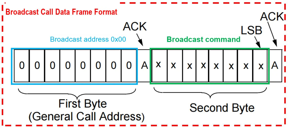
MCP4725 supports the following two broadcast call operations:
- General Reset (
General Call Reset): The second byte is00000110(06h). WhenMCP4725receives this command, it immediately aborts the current conversion operation and performs an internal reset, which is similar to a power-on reset (POR). After the reset, theMCP4725reloads the content from theEEPROMinto theDACregister, restoring to the initial power-on state. - General Call Wake-up: The second byte is
00001001(09h). When theMCP4725receives this command, it will reset the power-down data bits (PD1,PD2) in theDACregister to the normal operation mode (PD1,PD2= 0,0). This operation will not affect the power-down data bit settings in theEEPROM.
Multiple I2C buses may have multiple MCP4725 devices connected to them. The master device can send a broadcast command to reset or wake up all devices synchronously, thus simplifying the system initialization process.
1.3.7.2 High-Speed Mode
High-speed mode (HS Mode) is one of the three operating modes supported by the I2C protocol, which enables a faster data transfer rate to adapt to application scenarios requiring high throughput. HS Mode supports a maximum data transfer rate of 3.4 Mbit/s, significantly improving communication efficiency compared to the standard mode (100 kbit/s) and fast mode (400 kbit/s).
The I2C protocol requires that before entering high-speed mode, a special address byte 00001XXX must be sent to activate HS Mode, where XXX is the unique code of the high-speed master device (HS Master). The MCP4725 will not acknowledge (i. e., will not send ACK) after receiving this address byte, but will switch to HS Mode.
I2C The high-speed mode is commonly used in applications requiring high data transmission rates or multi-device communication, which can reduce bus occupancy time and improve system response speed.
2.8 PCB Routing Precautions
None.
III. Instructions for Circuit Engineering and Module Usage
3.1 Circuit Source Engineering
To obtain the source code of the circuit, please follow the official account [Freak Embedded]
3.2 Module Usage Instructions
The schematic diagram of this module is shown below:
SCH_Digital-to-Analog Conversion Module Based on MCP4725 Chip_v1.0_2025-11-22.pdf 2.3 MB
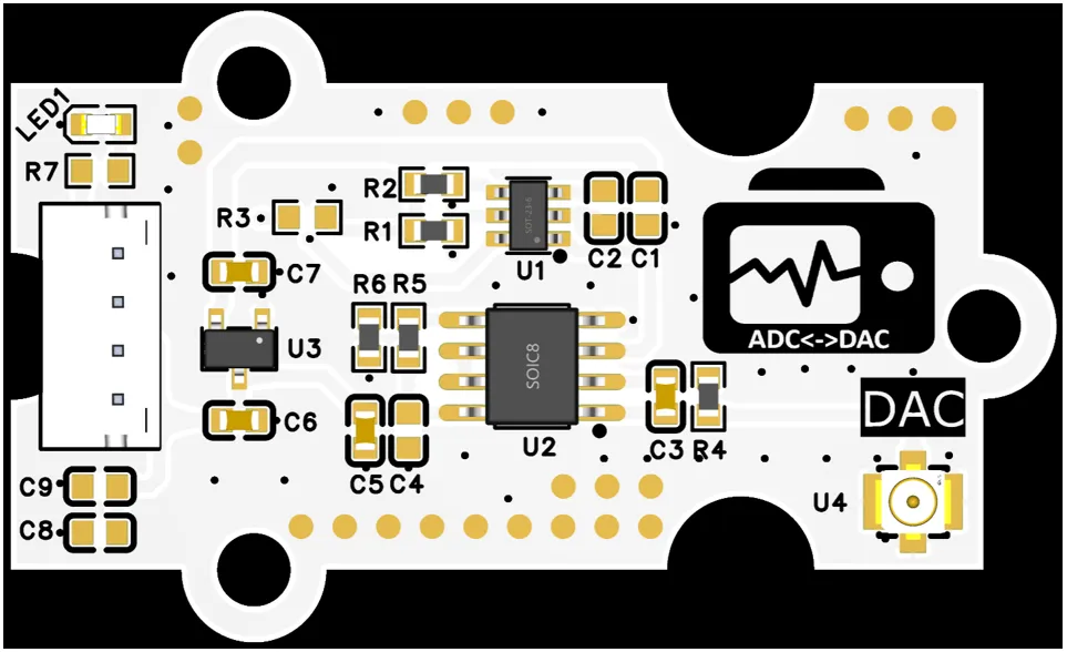
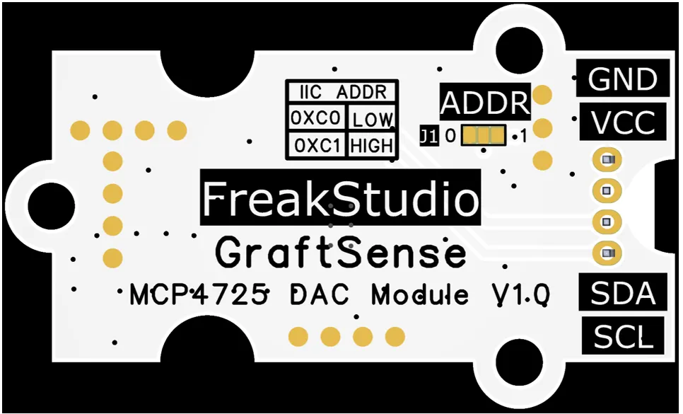
This module provides an I2C communication interface: it can be connected to the corresponding pins of MCU I2C peripherals for communication, and the ADDR short-circuit point allows setting the I2C address, which effectively avoids address conflicts during multi-device communication.
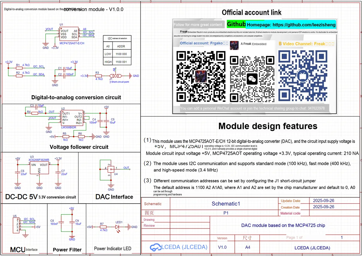
This circuit takes MCP4725 12-bit digital-to-analog converter (DAC) as its core, and is equipped with a voltage follower circuit to enhance the output load-carrying capability.
3.3 Application Experiment
Here, we use the GraftPort-RP2040 development board for testing, and the digital-to-analog conversion module based on the MCP4725 chip uses the I2C interface to communicate with the main controller.
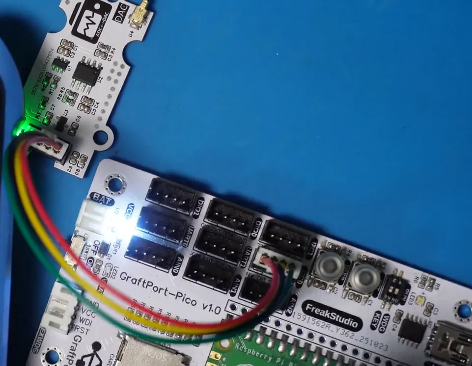
Here, we first use the HY2.0-4P cable to connect the module to the GraftPort-RP2040 development board's I2C0 interface:
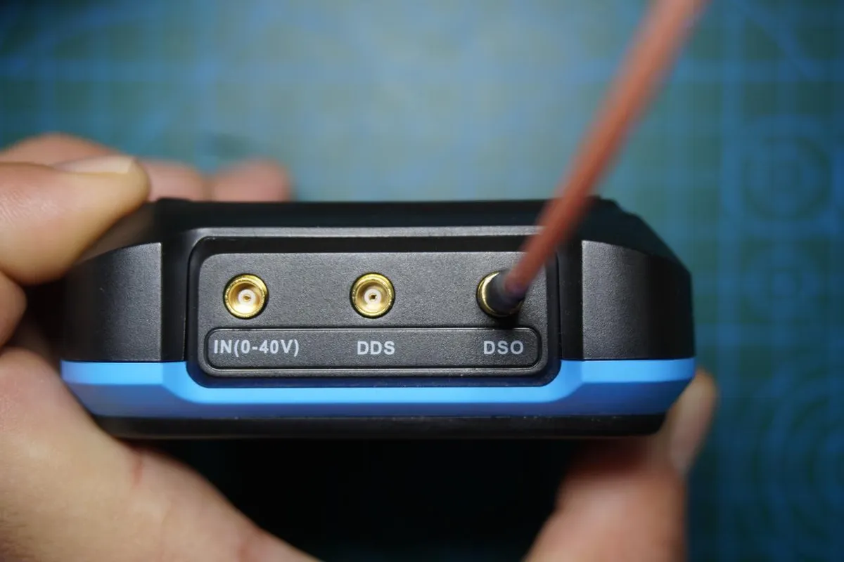
Next, use an IPEX -to- MCX RF cable to connect the DAC interface on the module and the signal acquisition of the handheld oscilloscope DSO via their respective MCX interfaces:
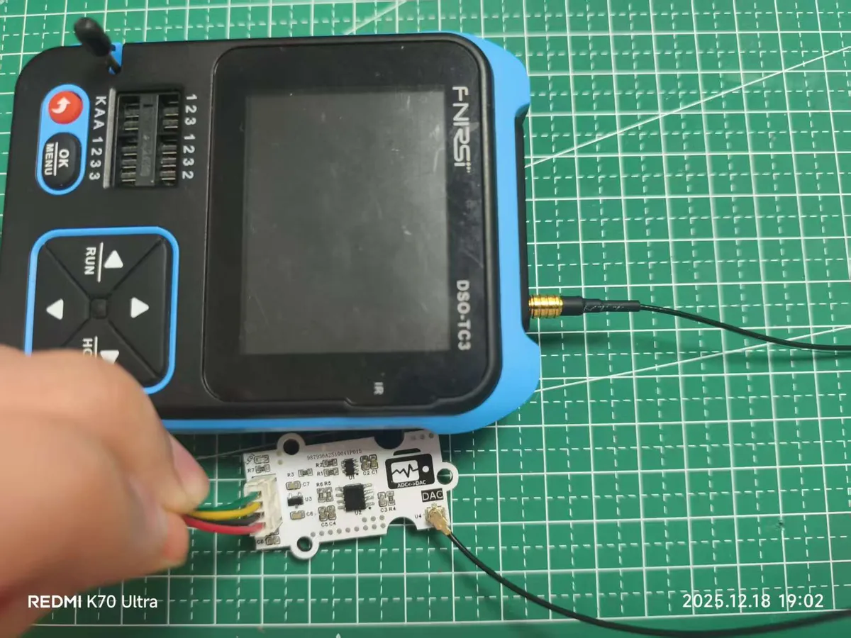
The module connections are shown in the following table:
Development Board Pins | Module (Digital-to-Analog Conversion Module Based on MCP4725 Chip) Pins | Description |
Pin 4 |
| I2C data transmission line, corresponding to |
Pin 5 |
| I2C clock signal line, corresponding to |
- |
|
|
Here, we need to search for relevant driver packages on uPyPI: https://upypi.net/zh/
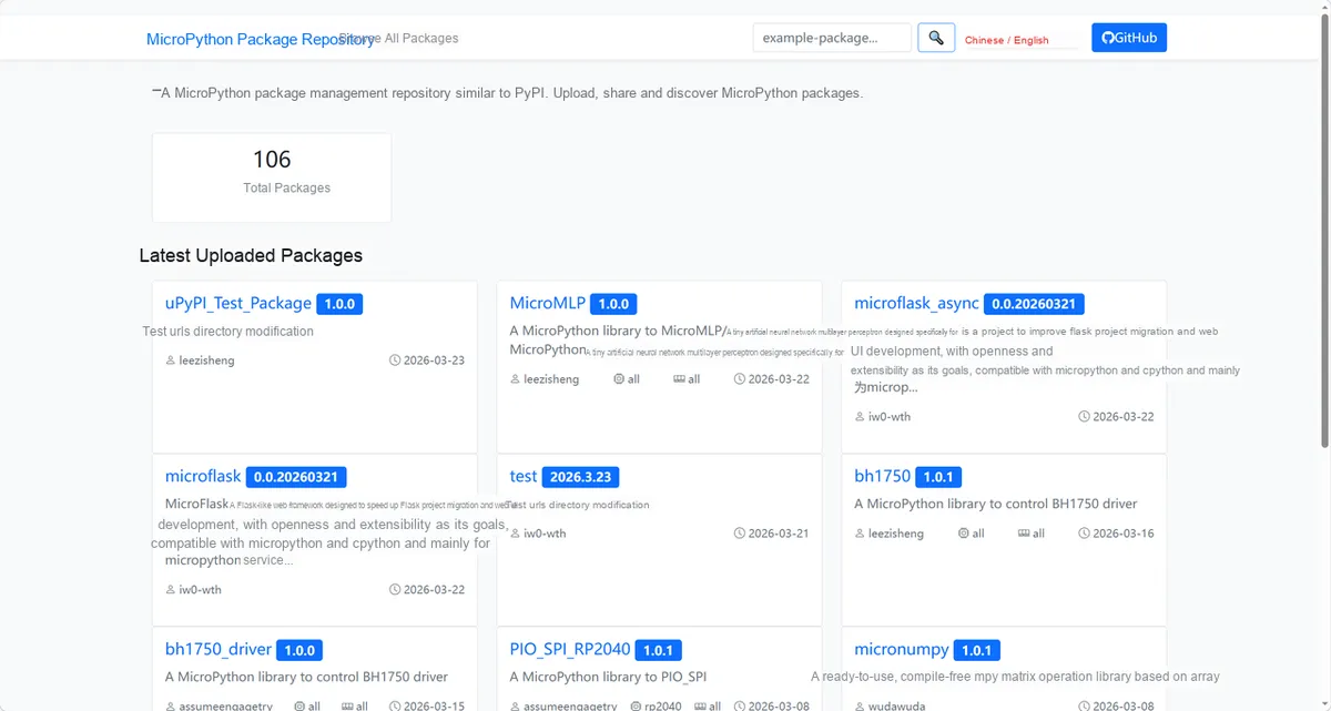
Enter mcp4725_driver to search, and the following will be displayed:

Click to copy the local installation command:
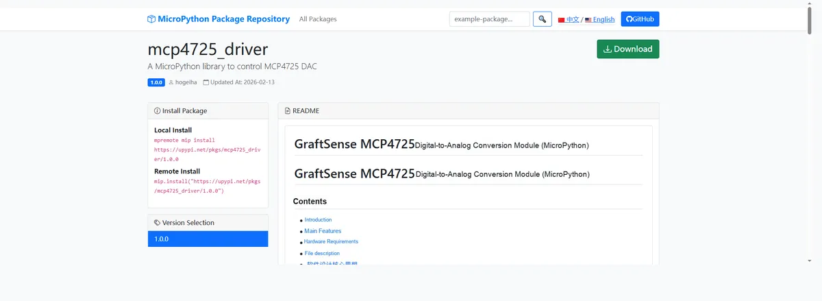
Here, we can use the mip tool to import module driver library code. Below are the usage commands for the mpremote tool:
mpremote mip install github:FreakStudioCN/GraftSense-Drivers-MicroPython/signal_generation/mcp4725_driverAfter importing the MicroPython driver code for the MCP4725 chip-based digital-to-analog conversion module, copy the following main.py code into our project:
In the following code, we generate a sine wave signal via an external DAC (MCP4725), read the voltage value through the ADC, and meanwhile transmit the voltage value via the serial port.
# Python env   : MicroPython v1.23.0
# -*- coding: utf-8 -*-
# @Time    : 2024/9/1 2:10 PM
# @Author  : Li Qingshui
# @File    : main.py
# @Description : DAC experiment, using an external DAC chip to generate a sine waveform

# ======================================== Import Modules ========================================

# Import the hardware module
from machine import ADC, Timer, Pin, I2C, UART
# Import time-related modules
import time
# Import the module for accessing and controlling MicroPython internals
import micropython
# Import the math library for calculating the sine wave
import math
# Import the mcp4725 module to control the DAC chip
from mcp4725 import MCP4725

# ======================================== Global Variables ============================================

# mcp4725 chip address
DAC_ADDRESS = 0x00
# Voltage conversion factor
adc_conversion_factor = 3.3 / (65535)

# ======================================== Functions ============================================

# Timer callback function
def timer_callback(timer: Timer) -> None:
    """
    Timer callback function, used to read ADC data periodically and call the user-defined callback function.

    Args:
        timer (machine.Timer): Timer instance.

    Returns:
        None
    """

    # Declare global variables
    global adc,adc_conversion_factor

    # Read ADC data
    value = adc.read_u16() * adc_conversion_factor
    # Call the user-defined callback function
    micropython.schedule(user_callback, (value))

# User-defined callback function
def user_callback(value: float) -> None:
    """
    User-defined callback function, used to process the voltage value sampled by the ADC and send it over the serial port.

    Args:
        value (float): Voltage value sampled by the ADC.

    Returns:
        None
    """
    # Declare global variables
    global uart

    # Get the floating-point number and round it to two decimal places
    formatted_value = "{:.2f}".format(value)
    # Send the sampled voltage data over the serial port
    uart.write(str(formatted_value) + '\r\n')
    # Print the sampled voltage data to the terminal
    print('dac generated voltage: ' + str(formatted_value))

# ======================================== Custom Classes ============================================

# ======================================== Initialization ==========================================

# Delay 3 s to wait for the device to finish powering up
time.sleep(3)
# Print debug information
print("FreakStudio : Using DAC to generate sine wave")

# Create a hardware I2C instance using the I2C1 peripheral, with a clock frequency of 400KHz, SDA pin 2, and SCL pin 3
i2c = I2C(id=0, sda=Pin(4), scl=Pin(5), freq=400000)

# Start scanning for devices on the I2C bus and return a list of slave addresses
devices_list = i2c.scan()
print('START I2C SCANNER')

# If devices_list is empty, no device is connected to the I2C bus
if len(devices_list) == 0:
    print("No i2c device !")
# If not empty, print the slave device addresses
else:
    print('i2c devices found:', len(devices_list))
    # Iterate over the slave device address list
    for device in devices_list:
        # If the device address is between 0x60 and 0x61, it is a DAC chip
        if 0x60 <= device <= 0x61:
            print("I2C hexadecimal address: ", hex(device))
            DAC_ADDRESS = device

# Create the DAC object, using the I2C0 peripheral, with address DAC_ADDRESS
dac = MCP4725(i2c, DAC_ADDRESS)
# Read the DAC configuration information
eeprom_write_busy, power_down, value, eeprom_power_down, eeprom_value = dac.read()
print(eeprom_write_busy, power_down, value, eeprom_power_down, eeprom_value)
# Configure the DAC: cancel power-down mode, output voltage 0V, write to EEPROM
dac.config(power_down='Off',value=0,eeprom=True)
# Delay 50ms; reading immediately after configuration causes an error
time.sleep_ms(50)
# Read the DAC configuration information
eeprom_write_busy, power_down, value, eeprom_power_down, eeprom_value = dac.read()
print(eeprom_write_busy, power_down, value, eeprom_power_down, eeprom_value)

# Create the ADC instance: ADC1-GP27
adc = ADC(1)
# Create a software timer object
timer = Timer(-1)
# Start the timer, triggering the timer_callback function every 5ms to sample voltage with the ADC
timer.init(period=5, mode=Timer.PERIODIC, callback=timer_callback)

# Create the serial port object, set the baud rate to 115200
uart = UART(0, 115200)
# Initialize the uart object with a baud rate of 115200, 8 data bits, no parity bit, and 1 stop bit
# Set the serial port timeout to 100ms
uart.init(baudrate  = 115200,
          bits      = 8,
          parity    = None,
          stop      = 1,
          tx        = 0,
          rx        = 1,
          timeout   = 100)

# ========================================  Main Program  ===========================================

# Generate the sine wave
for i in range(10000):
    # Calculate the voltage value of the sine wave
    value = 3.3 * math.sin(2 * math.pi * i / 100) + 3.3
    # Convert the voltage value of the sine wave to an integer
    value = int(value * 4095 / 6.6)
    # Write the analog value to the DAC
    dac.write(value)
    # Delay 10ms
    time.sleep_ms(10)

# Stop ADC sampling
timer.deinit()
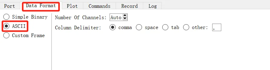
Open SerialPlot software, select the corresponding port connected to the USB to TTL chip, and click the Open button:

Data Format Selection ASCII encoding, with other configurations left as default:
3.1 Application Experiment - PC Software Configuration.mp4 627 KB
To flash the code, open a terminal and use the mpremote tool to connect to the main controller; the output is as follows:
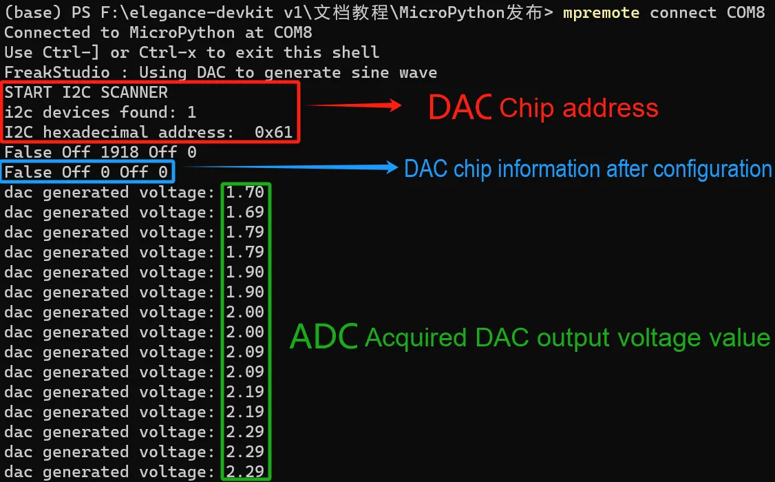
As can be seen, the DAC chip MCP4725 has an address of 0x60, and the configuration and method of the DAC chip can work properly.
Open SerialPlot software, and you can see that the displayed DAC output voltage is a sine curve.
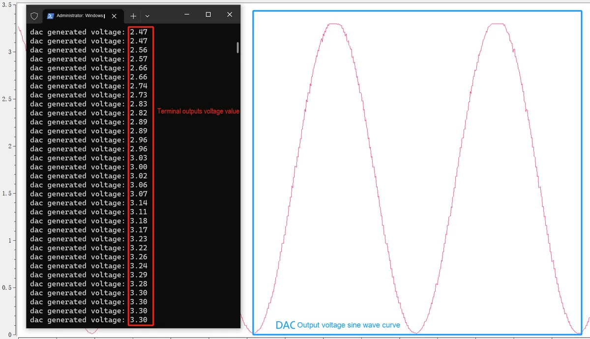
Connect the signal to an oscilloscope to view the waveform
IV. Drivers
mcp4725_driver.zip 7 KB
5. BOM & Recommended Alternative Parts
None.
VI. Revision History
Document Version | Date of Revision | Modifier | Revised Content |
v1.0 | 2025-11-22 | Li Zisheng | Initialize the document The BOM sheet has not been finally checked, the driver has not been re-verified, and the 3.3 application experiment Not yet specified. |
v1.1 | 2025-12-29 | Li Zisheng | Added application experiments and production files |
v1.2 | 2025-12-31 | Xin Ruili | Create an open version of the document based on the internal document version v1.1. |
v1.3 | 2026-03-29 | Xin Ruili | Modified the application experiment section |
VII. Relevant Materials
7.1 Chip Datasheet
7.2 Unique Icons for PCB Silk Screen