Contents
- I. Module Introduction
- 2. Introduction to Main Chips
- 2.1 Chip Overview
- 2.2 Pin Definition
- 2.3 Functional Block Diagram
- 2.4 Performance Parameters
- 2.5 Reference Circuit
- 2.6 Chip Configuration
- 2.7 Communication Interfaces and Related Protocols
- 2.8 PCB Routing Precautions
- III. Instructions for Circuit Engineering and Module Usage
- 3.1 Circuit Source Engineering
- 3.2 Module Usage Instructions
- 3.3 Application Experiment
- 4. Drivers
- 5. BOM & Recommended Alternative Parts
- VI. Revision History
- VII. Relevant Materials
- 7.1 Chip Datasheet
- 7.2 Unique Icons for PCB Silk Screen
I. Module Introduction
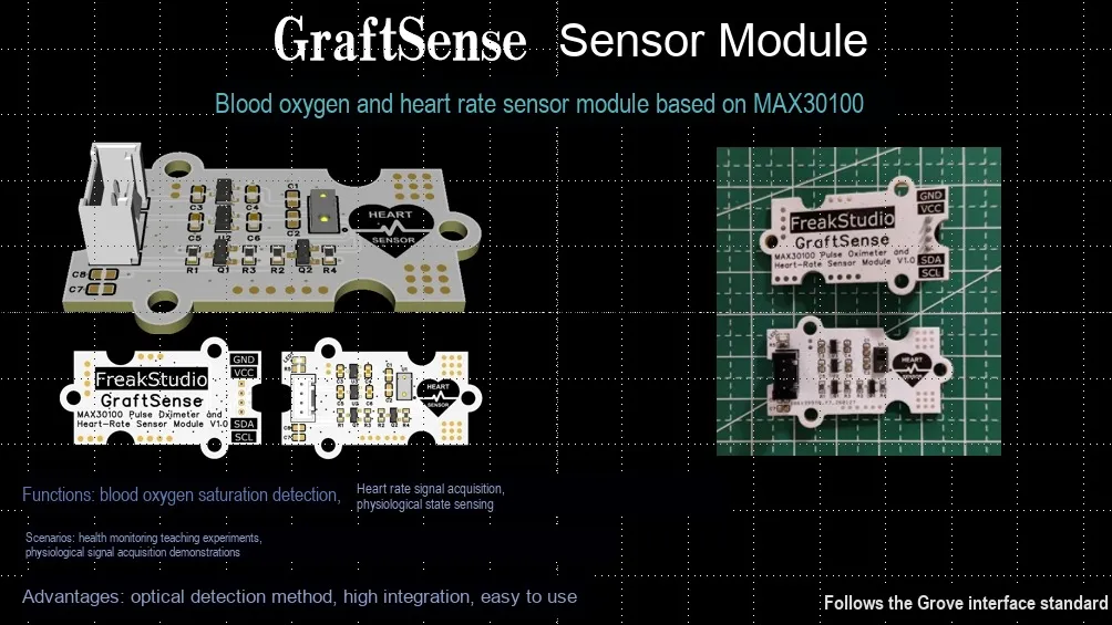
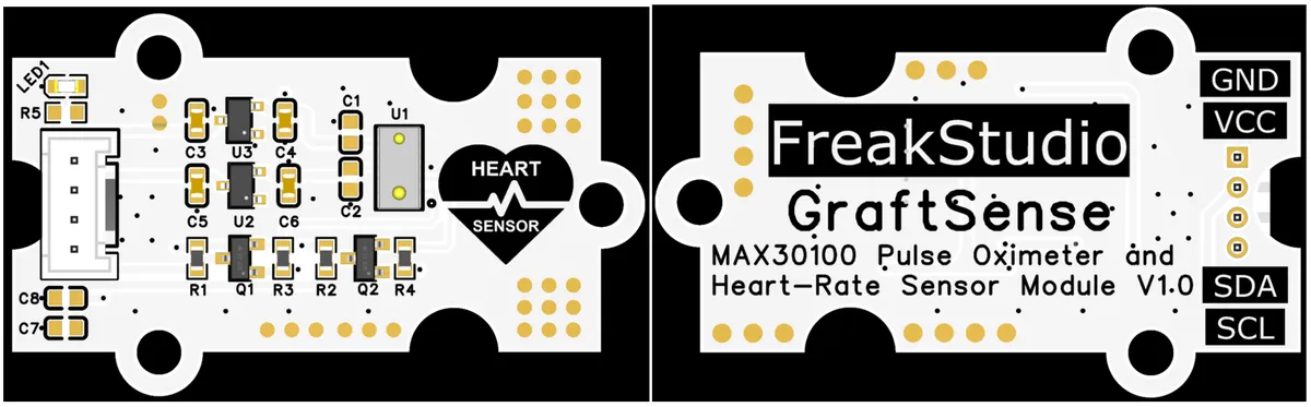
The heart rate and blood oxygen sensor module based on MAX30100 is a physiological signal acquisition module with the MAX30100 chip as the core, supports the I2C communication interface, and can accurately collect and output data related to heart rate and blood oxygen concentration;This module integrates 5V-to-3.3V and 5V-to-1.8V DC-DC conversion circuits, a 3.3V-to-1.8V level shifting circuit, a power filter circuit and a power indicator. The main power supply voltage ranges from 1.7V to 1.8V, the LED power supply voltage ranges from 3.1V to 5.0V, the typical current in operating mode is approximately 600μA, and the typical current in sleep mode is only 0.7μA, featuring low power consumption and stable power supply;The device address is 0xAE, the read address is 0xAF, I2C clock frequency supports 0~400kHz, it also features ambient light rejection (ALR) and anti-interference design, which can work stably under strong light environment of 100Klux; equipped with standard I2C interface and mounting holes, it is suitable for scenarios such as wearable health bands, portable heart rate and oximetry monitors, and household health monitoring devices, enabling convenient continuous monitoring of physiological indicators.
2. Introduction to Main Chips
2.1 Chip Overview
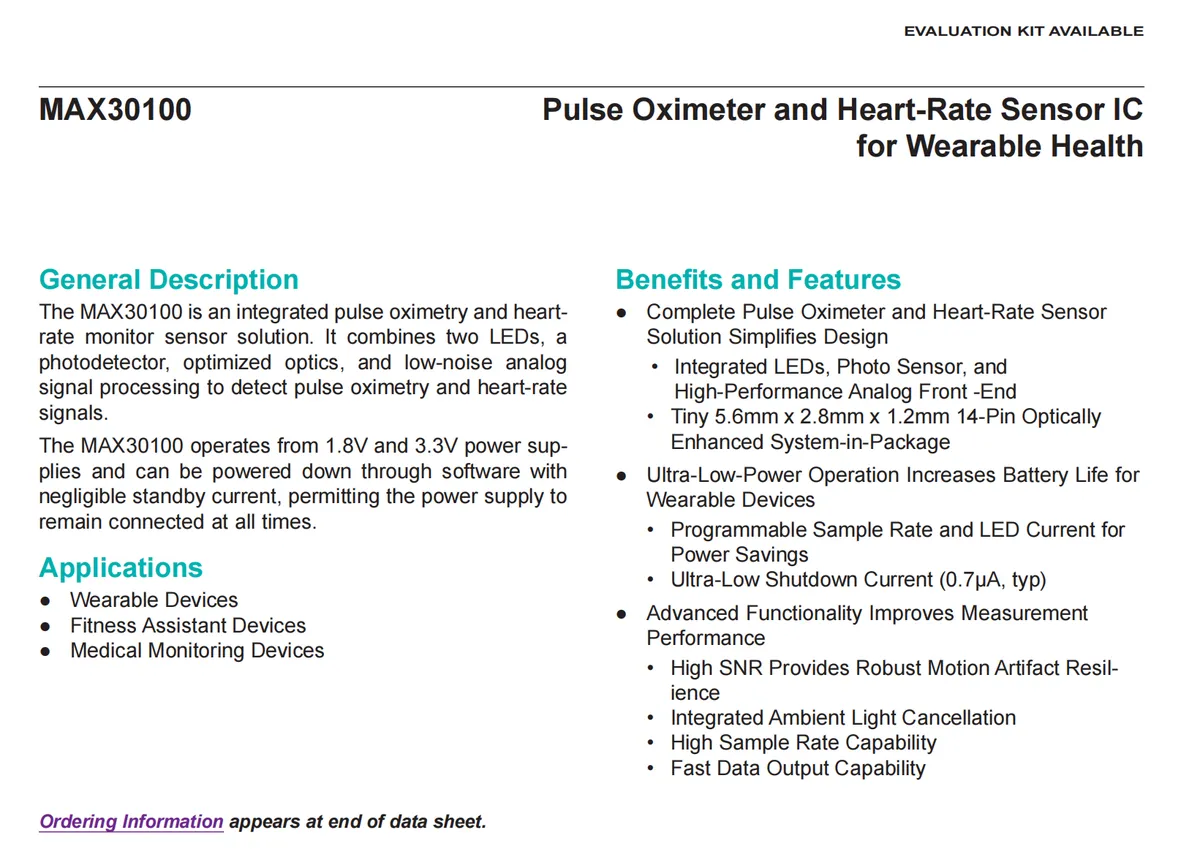
MAX30100 is an integrated pulse oximetry and heart rate monitoring sensor chip designed specifically for wearable health scenarios. It integrates two LEDs, a photodetector, optimized optical components, and a low-noise analog signal processing circuit, capable of directly detecting and outputting blood oxygen saturation and heart rate signals; the chip supports dual power supplies of 1.8V and 3.3V, and can achieve low-power shutdown via software. Its typical current in sleep mode is only 0.7μA, allowing the power supply to remain connected for a long time with almost no power consumption;It features a high signal-to-noise ratio, effectively resists motion artifacts, integrates ambient light suppression, supports programmable sampling rate and LED current to optimize power consumption, and boasts high sampling rate and fast data output capability; adopting a compact 14-pin optical-enhanced system-in-package measuring 5.6mm×2.8mm×1.2mm, it simplifies the design of terminal devices, is suitable for scenarios such as wearable devices, fitness assistance devices and medical monitoring devices, and can effectively extend the battery life of wearable devices.
2.2 Pin Definition
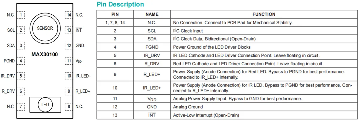
The pins of the MAX30100 can be categorized into several types according to their functions, as briefly described below:
- No-connection pins (1,7, 8,14): These are only for mechanical fixation; simply connect them to the PCB pads, no electrical connection is required.
- I2C communication pins:
SCL(Pin 2) serves as theI2Cclock input, andSDA(Pin 3) is a bidirectionalI2Cdata pin (open-drain output). - Power and Ground Pins: VDD (Pin 11) is the analog power input, GND (Pin 12) is the analog ground,
PGND(Pin 4) is the power ground for theLEDdriver module. - LED Driver Pins:
IR_DRV(Pin 5) andR_DRV(Pin 6) are the cathode driving terminals for the infrared and red LEDs respectively (left floating in the circuit);R_LED+(Pin 9) andIR_LED+(Pin 10) are the anode power supply terminals for the red and infrared LEDs respectively (internally connected to each other). - Interrupt Pin:
INT(Pin 13) is an active-low interrupt output (open-drain output).
2.3 Functional Block Diagram
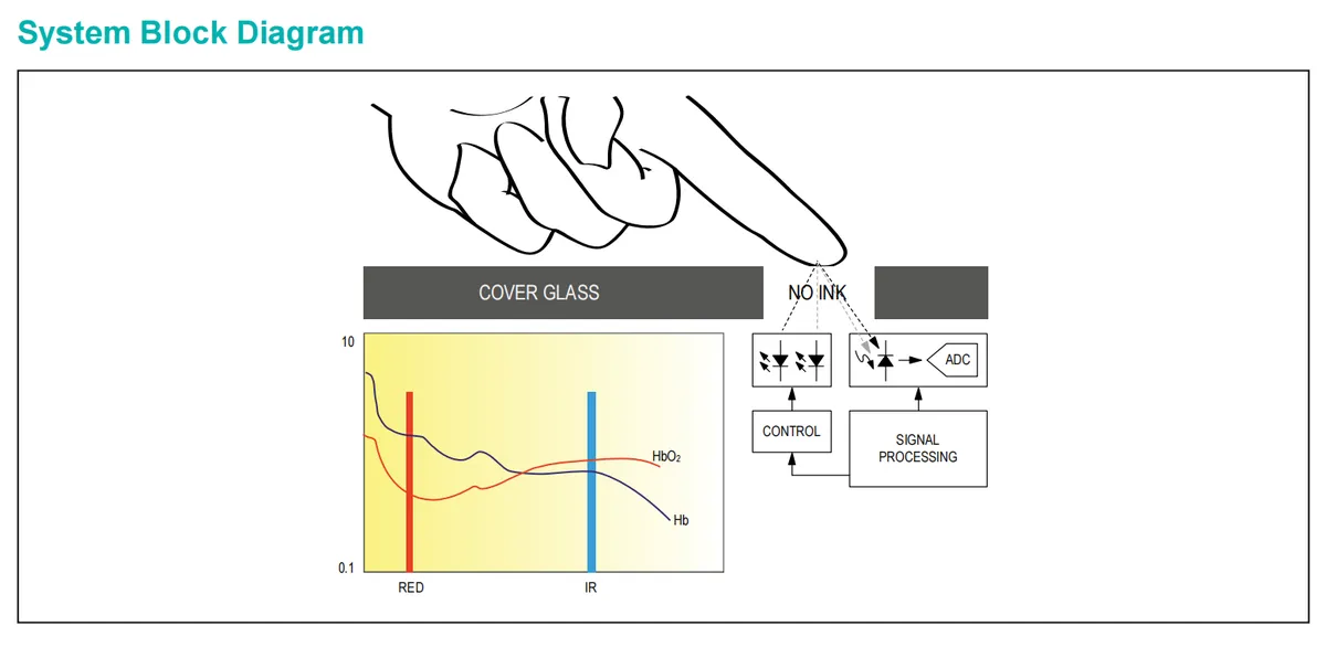
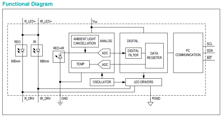
The functional block diagram of the MAX30100 illustrates its complete working process from optical signal transmission to data output:
- The LED driver module inside the chip drives the red (660nm) and infrared (880nm) LEDs to emit pulsed light of specific wavelengths, which penetrate the skin and are then received by the photodetector.
- The signal output by the detector enters the analog processing unit, where ambient light interference is first eliminated via the Ambient Light Cancellation (ALC) circuit, before being converted into a digital signal by a 16-bit Σ-Δ ADC.
- The digital signal is processed by the built-in discrete-time filter and then stored in the data register. Meanwhile, the on-chip temperature sensor collects temperature data to compensate for environmental errors in blood oxygen calculation.
- Finally, the processed heart rate, blood oxygen and temperature data can be output to an external main control device via the I2C communication interface (SCL clock, SDA data), and can also actively trigger external notifications through the interrupt pin (INT).
The entire system is clocked by an internal oscillator, and supports software-configurable parameters such as LED current, pulse width and sampling rate, which optimizes power consumption while ensuring monitoring accuracy to adapt to the low-power requirements of wearable devices.
2.4 Performance Parameters
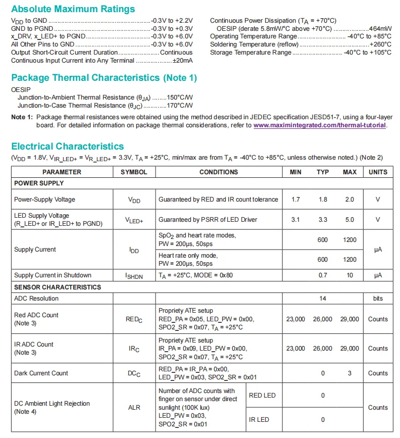
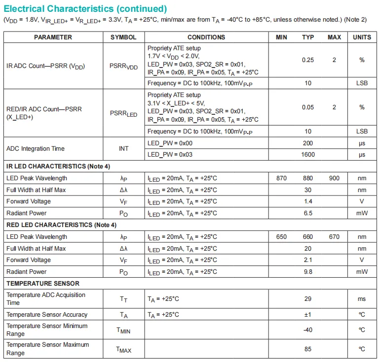
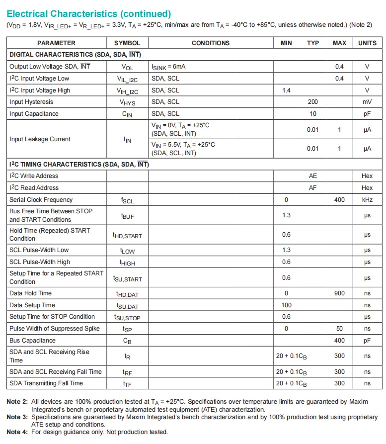
The key parameters of the MAX30100 cover core dimensions including power supply, sensors, communication and environmental adaptation:
- In terms of power supply, the main power supply VDD ranges from 1.7V to 2.0V (typical value: 1.8V);
- The VLED+ range of the LED driver power supply is 3.1V~5.0V (typical value: 3.3V), with a typical current of 600μA in operating mode and merely 0.7μA in sleep mode, featuring both flexible power supply and low power consumption.
Sensor Performance:
- Equipped with a 14-bit resolution ADC, the typical ADC counts for both red light and infrared light are 26000 Counts, the dark current count is 0 Counts, and it features ambient light suppression capability under strong light of 100Klux;
- It also integrates an on-chip temperature sensor with an accuracy of ±1℃, which can compensate for the environmental errors in blood oxygen calculation.
- In terms of LED characteristics, the typical wavelength of red LED is 660nm, and that of infrared LED is 880nm. It supports programmable LED current ranging from 0 to 50mA and programmable pulse width ranging from 200μs to 1.6ms, making it adaptable to different monitoring scenarios.
In terms of communication, this device adopts the I2C interface, with a device write address of 0xAE and a read address of 0xAF, supports a clock frequency ranging from 0 to 400kHz, features a typical output low voltage of 0.4V and an input capacitance of 10pF to ensure stable communication; in terms of environmental adaptability, both its operating and storage temperature ranges are -40℃ to + 85℃, making it compatible with complex application scenarios of wearable devices.
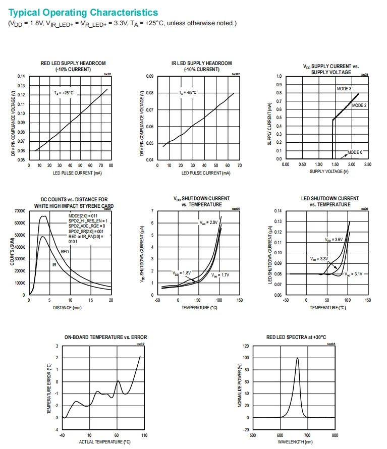
These typical operating characteristic curves illustrate MAX30100 the performance variation trends under different conditions such as voltage, temperature, current and distance, which can help engineers evaluate and optimize the operating status of the module in practical designs.
- Red LED power supply margin (10% current): Displays the change in the power supply margin of the red LED under different LED pulse currents; the higher the current, the higher the power supply margin.
- Power Margin of Infrared LED (10% Current): This presents the relationship between the pulse current of the infrared LED and its power margin, where the power margin increases as the current rises.
- VDD Supply Current vs. Supply Voltage: This graph illustrates the variation of the main power supply current with the supply voltage under different operating modes; the current will rise in a step-like manner once the voltage increases to the threshold.
- DC count vs. distance for high-impact polystyrene cover: This plot demonstrates the variation of DC counts of red light and infrared light with detection distance. At close range, the counts rise rapidly and then fall back, reflecting the attenuation characteristic of optical signals.
- VDD Shutdown Current vs. Temperature: This graph illustrates the variation of the chip's shutdown current with temperature under different VDD voltages. The higher the temperature, the greater the shutdown current, and the current increase is more pronounced at higher voltages.
- LED turn-off current vs. temperature: This graph illustrates the variation of LED turn-off current with temperature under different VLED+ voltages. The current rises significantly as temperature increases, with a more pronounced growth rate at higher voltages.
- On-board Temperature vs. Error: This graph illustrates how the measurement error of the on-board temperature sensor varies with the actual temperature. The error remains relatively small in the low and medium temperature ranges, and increases to some extent in the high temperature range.
- Red light spectrum at 30℃: This diagram illustrates the normalized radiant power distribution of a red LED as a function of wavelength at 30℃, with the peak appearing at approximately 660nm, which aligns with the typical wavelength characteristics of red LEDs.
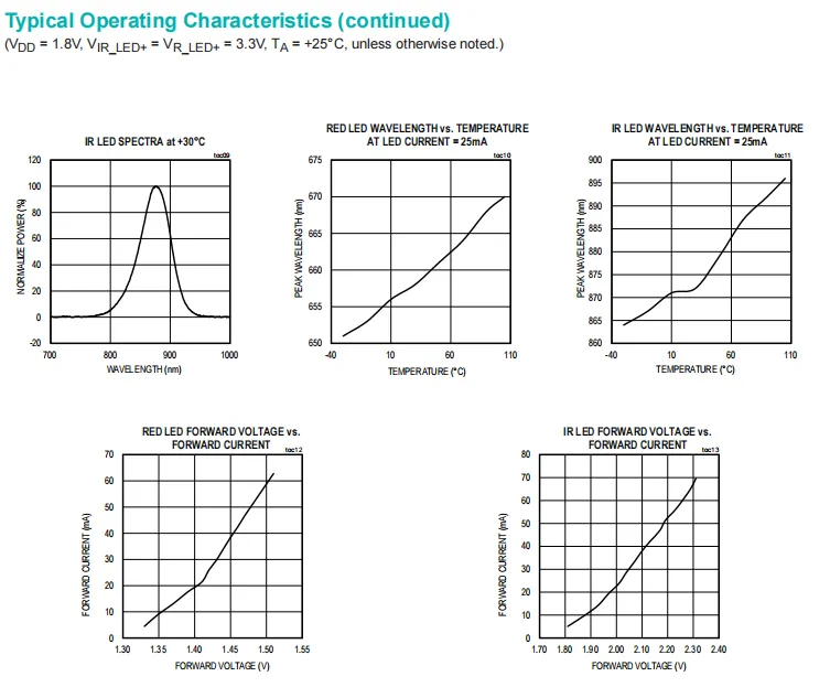
These typical operating characteristic curves focus on the LED optical and electrical properties of the MAX30100, reflect the variation law of its performance with conditions such as temperature and current, and serve as an important basis for optical and driver circuit design:
- Infrared LED Spectrum at 30°C: It shows the distribution of normalized radiant power of the infrared LED versus wavelength at 30°C, with a peak around 880nm, which conforms to its typical optical characteristics.
- Red LED Wavelength vs. Temperature (at 25 mA Current): This demonstrates how the peak wavelength of a red LED changes with temperature; as the temperature rises, the wavelength shifts toward the longer wavelength range.
- Infrared LED Wavelength vs. Temperature (at 25 mA Current): This demonstrates how the peak wavelength of an infrared LED changes with temperature: as the temperature rises, the wavelength also shifts toward the longer wavelength range.
- Forward Voltage vs. Forward Current of Red LED: It shows an approximately linear relationship between the forward voltage and forward current of the red LED: the higher the current, the higher the forward voltage.
- Infrared LED Forward Voltage vs. Forward Current: This graph demonstrates the approximately linear relationship between the forward voltage and forward current of an infrared LED — the higher the current, the higher the forward voltage.
2.5 Reference Circuit
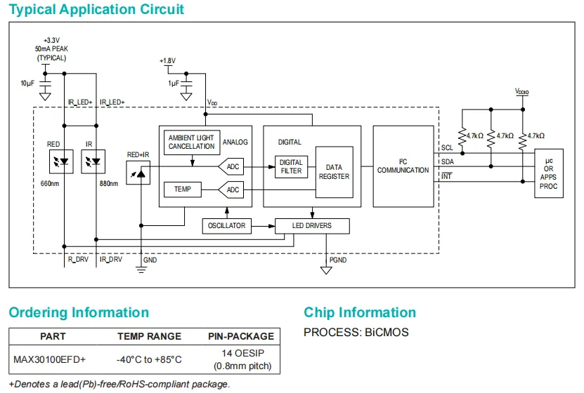
The typical reference circuit design of the MAX30100 is concise, and only a small number of external components are required to realize its full functions:
- The main power supply VDD is powered by 1.8V and externally connected with a 1μF capacitor for filtering; the LED driving power supply VLED+ is powered by 3.3V and externally connected with a 10μF capacitor to stabilize the voltage;
- The anodes of the red light (660nm) and infrared (880nm) LEDs are connected to VLED+, their cathodes are respectively connected to the R_DRV and IR_DRV pins of the chip, and are controlled by the internal LED driver module;
- The I2C communication interface (SCL, SDA, INT) is connected to the external master device via 4.7kΩ pull-up resistors to ensure stable signal levels.
The chip has integrated functional modules such as ambient light suppression, ADC conversion, and digital filtering, which can complete the acquisition, processing and output of heart rate and blood oxygen signals without additional complex circuits, and the overall circuit adapts to the design requirements of miniaturization and low power consumption of wearable devices.
2.6 Chip Configuration
None.
2.7 Communication Interfaces and Related Protocols
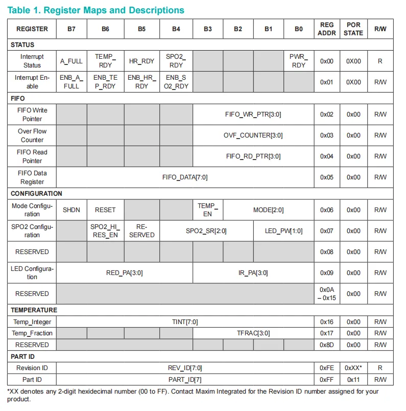
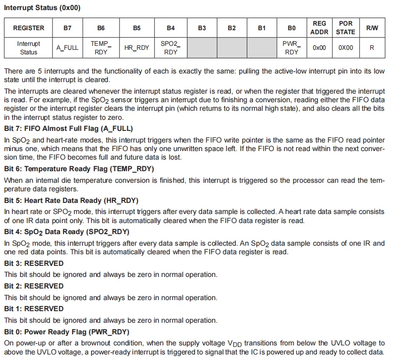
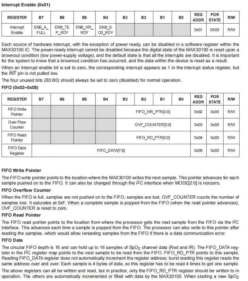
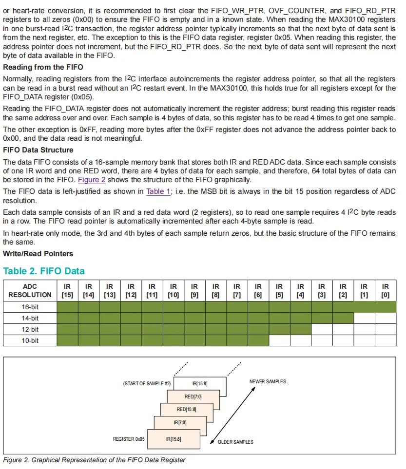
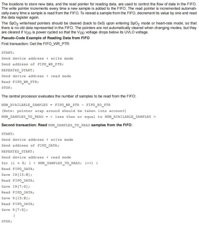
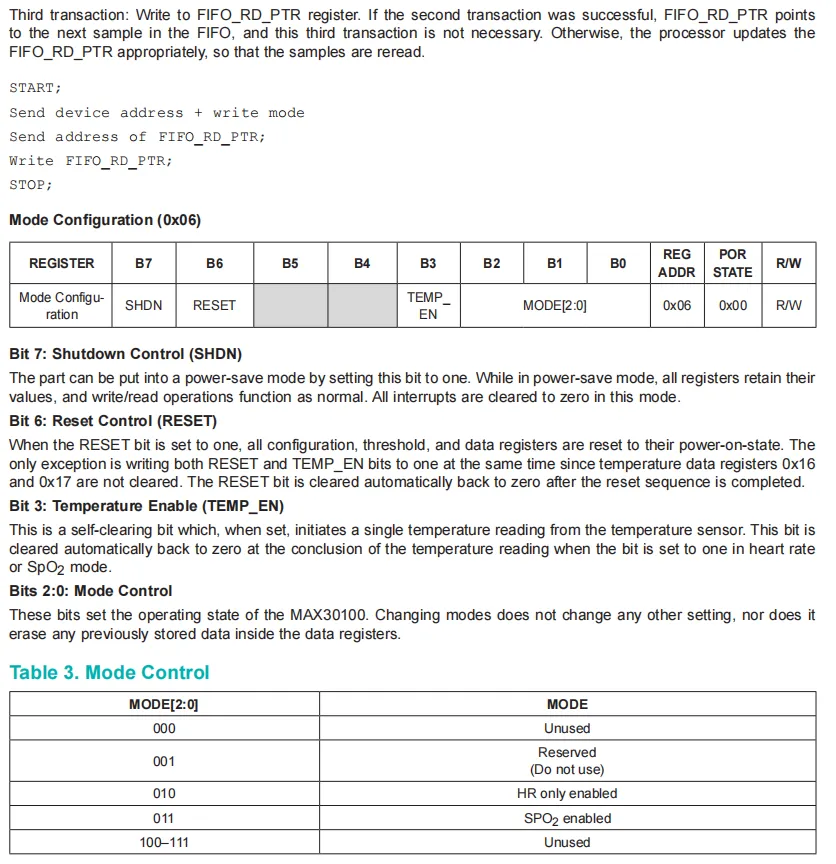
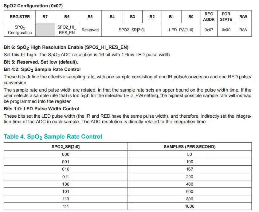
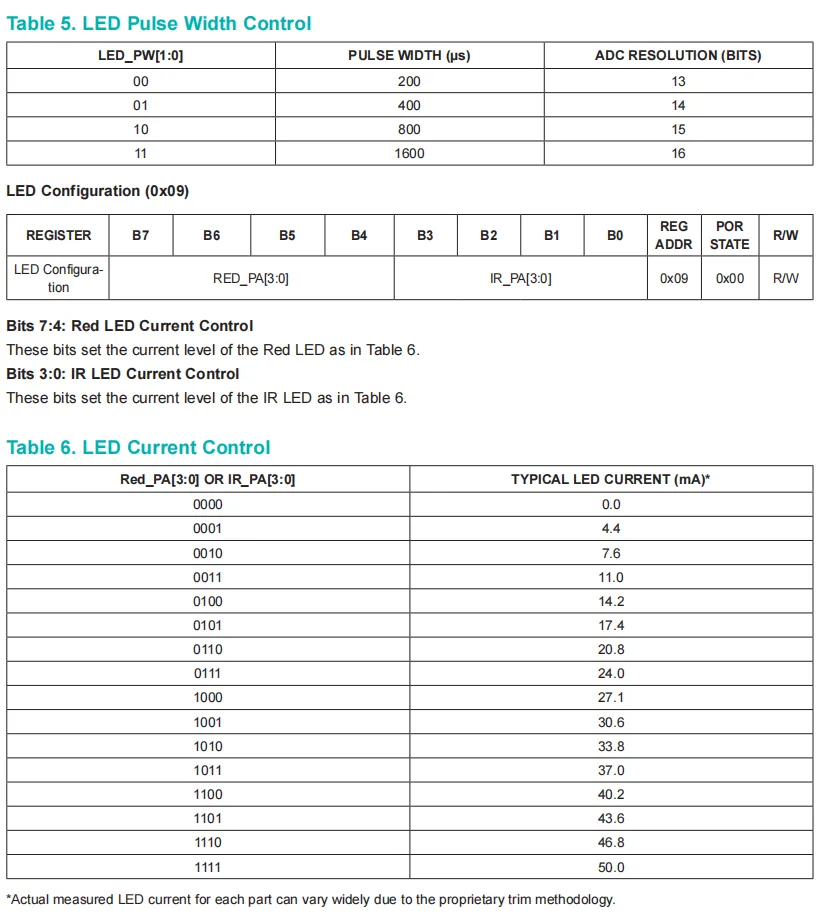
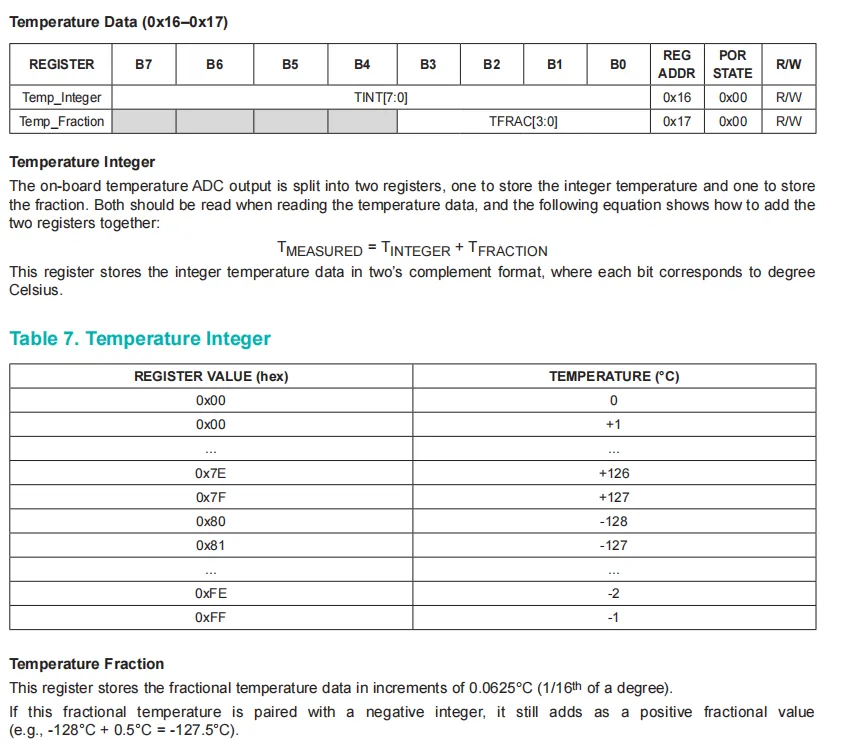
The MAX30100 implements full functional control and data interaction through a structured register system, which is accessible via the I2C interface and covers core functions including status and interrupt management, FIFO data buffering, operating mode configuration, LED parameter adjustment, temperature data reading, and device identification.
- The Interrupt Status Register (0x00) indicates events such as FIFO full, temperature/heart rate/blood oxygen data ready, etc. , while the Interrupt Enable Register (0x01) allows configuration of the enable/disable status of each interrupt.
- The FIFO module manages a 16-sample ring buffer via the read/write pointers (0x02,0x04), overflow counter (0x03) and data register (0x05); each sample contains infrared and red light ADC data, which requires 4 I2C read operations to acquire in full, and the module supports pointer wrap-around and repeated reading.
- Among the configuration registers, the mode configuration register (0x06) can set power-off, reset, temperature enable and operation mode (heart rate only / SpO2 mode); the SpO2 configuration register (0x07) adjusts the sampling rate (50~1000 times/second), LED pulse width (200~1600μs, corresponding to 13~16-bit ADC resolution) and high-resolution mode; the LED configuration register (0x09) can set the drive current (0~50mA) of the red/infrared LED;
- Temperature data is obtained via the integer (0x16) and fractional (0x17) registers, with a precision of 0.0625°C;
- The device ID register (0xFF) is used to identify the model and version of the chip.
The entire register system supports flexible software configuration to adapt to the requirements of low power consumption and multi-scenario monitoring for wearable devices.
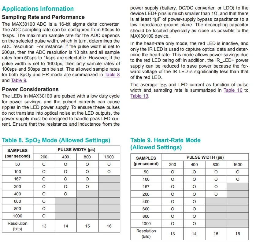
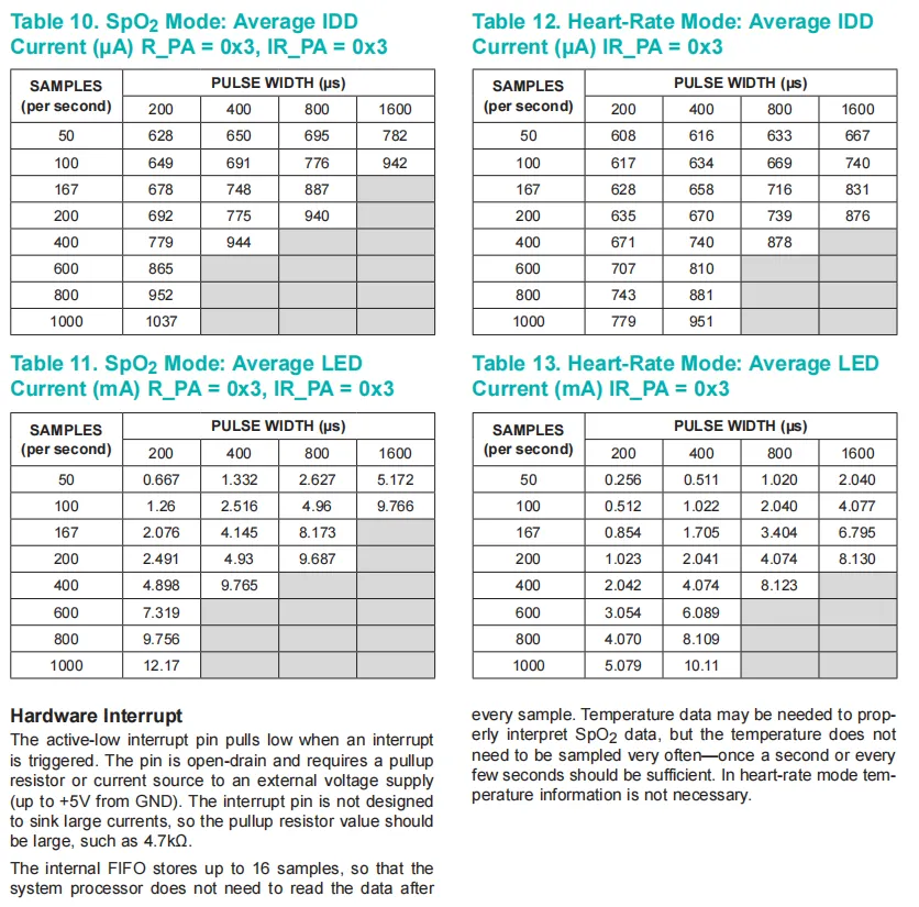
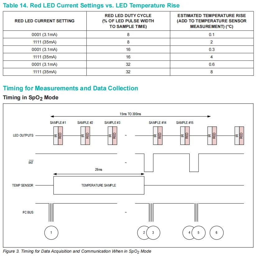
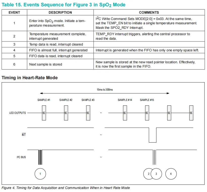

This section elaborates on the key design and operational details of the MAX30100 in practical applications:
- In terms of sampling rate and performance, its 16-bit Σ-Δ ADC supports sampling rates ranging from 50 sps to 1 ksps. The sampling rate is strongly correlated with the LED pulse width, which determines the ADC resolution (13 to 16 bits), and there are respective allowable configuration combinations for the blood oxygen and heart rate modes.
- The power supply design shall take into account the peak current brought by the low-duty-cycle pulse driving of the LED, and shall be matched with a low-impedance power supply and a decoupling capacitor; in the heart rate mode, the red LED can also be turned off and the power supply of the infrared LED can be reduced to further save energy;
- Quantified data are available for the average IDD current, LED current and LED temperature rise amplitude corresponding to different modes, sampling rates and pulse widths, which can serve as a reference for power consumption and thermal design.
- The interrupt mechanism adopts active-low open-drain output, which requires an external pull-up resistor; the blood oxygen and heart rate modes respectively define the event timing and procedures covering links such as temperature sampling, FIFO full interrupt, and data reading.
For power-on, it is recommended to activate VDD first before supplying power to the LEDs; communication is realized via the I2C interface compatible with SMBus, which supports a maximum clock frequency of 400kHz and complies with the standard START/STOP and acknowledge protocols.
2.8 PCB Routing Precautions
None.
III. Instructions for Circuit Engineering and Module Usage
3.1 Circuit Source Engineering
To obtain the circuit source project, please follow the official account [Freak Embedded].
3.2 Module Usage Instructions
The schematic diagram of this module is shown below:
SCH_Blood Oxygen and Heart Rate Sensor Module Based on MAX30100_v1.0.pdf 3.0 MB
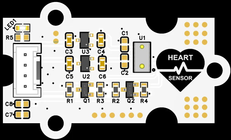
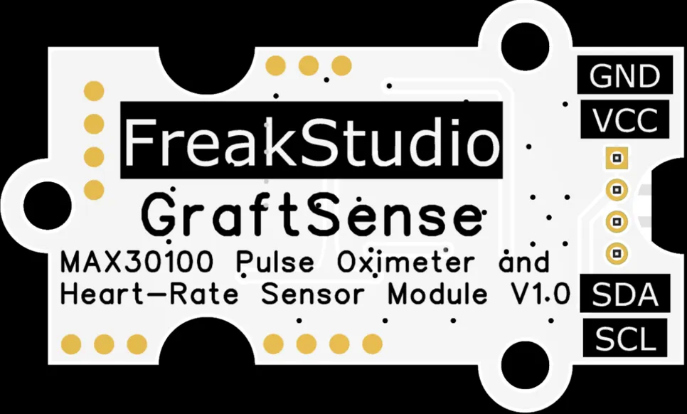
This module provides an I2C communication interface that supports standard I2C communication rates, with a default slave address configured as 0x57 for I2C. It is compatible with 3.3V system logic levels to adapt to mainstream microcontrollers, can stably transmit the heart rate and blood oxygen digital data corresponding to red light and infrared light detection, and is suitable for scenarios such as health monitoring devices and wearable maker projects, providing a convenient hardware connection solution for the digital collection of physiological parameters and system interaction.
During use, you need to keep the pad of your finger pressed continuously on the position shown in the diagram below to measure heart rate and blood oxygen-related data more accurately:
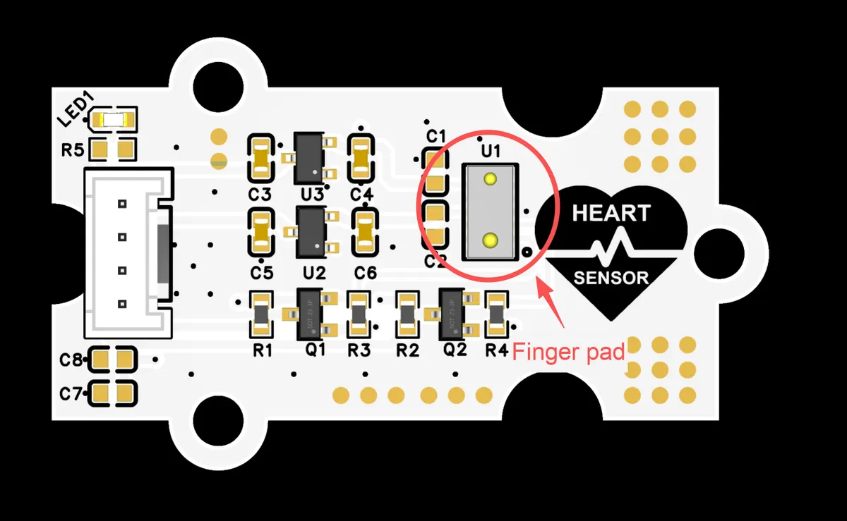
Please note the following points when using it:
- Attach the sensor firmly to the skin (favorable sites include the pad of a finger, earlobe, etc.) to avoid gaps or hair blocking the optical window; do not cover the sensor with your fingernail (fingernails are opaque and will block light transmission), and keep the skin at the attachment site as flat as possible during wear.
- Avoid direct exposure of the sensor to strong light (sunlight, intense artificial lighting), as ambient light will interfere with the optical signal; remain stationary during measurement, as movement or shaking will cause fluctuations in light intensity data and lead to distorted heart rate / blood oxygen calculations.
- This module features consumer-grade accuracy and cannot be used as a basis for medical diagnosis. Keep the optical window of the sensor clean (stains or fingerprints will block light) and wipe it gently after prolonged use.
3.3 Application Experiment
Here, we use the GraftPort-RP2040 development board for testing, and the MAX30100-based blood oxygen and heart rate sensor module uses the I2C interface to communicate with the main controller.
Here, we first use the HY2.0-4P cable to connect the module to the GraftPort-RP2040 development board's I2C0 interface:
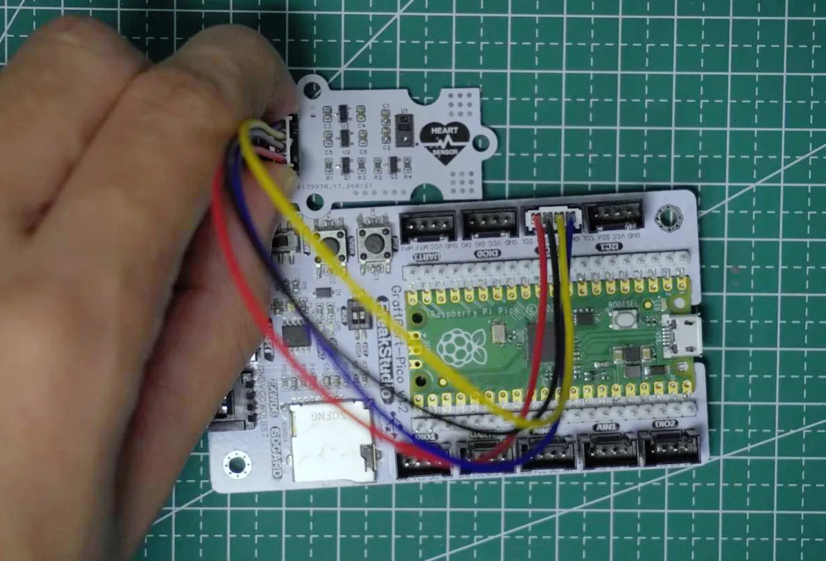
The module connections are shown in the following table:
Development Board Pins | Module Pins | Description |
Pin 4 |
|
|
Pin 5 |
|
|
Here, we need to search for the relevant driver packages on uPyPI: https://upypi.net/zh/

Enter max30100_driver to search, and the following will be displayed:

Click to copy the local installation command:

Here, we can import the module driver library code via the mip tool. The following are the usage commands for the mpremote tool:
mpremote mip install github:FreakStudioCN/GraftSense-Drivers-MicroPython/sensors/max30100_driverImport the oximeter sensor module based on the MAX30100 chip - MicroPython driver code, then copy the following main.py code into our project:
# Python env   : MicroPython v1.27.0
# -*- coding: utf-8 -*-
# @Time    : 2026/02/03 11:00
# @Author  : hogeiha
# @File    : main.py
# @Description : MAX30100 IR + red + blood oxygen reading and calculation example

# ======================================== Import Modules =========================================

from machine import I2C, Pin
import max30100
import time

# ======================================== Global Variables ============================================

# ======================================== Functions ============================================

# ======================================== Custom Classes ============================================

# ======================================== Initialization ==========================================

# Power-on delay of 3 s
time.sleep(3)
# Print debug message
print("FreakStudio: Use the MAX30100 to read values and calculate blood oxygen levels..")

# I2C: SDA=GP4, SCL=GP5
i2c = I2C(0, scl=Pin((5)), sda=Pin((4)))

# Start scanning for devices on the I2C bus and return a list of slave addresses
devices_list: list[int] = i2c.scan()
print('START I2C SCANNER')
# If the devices list is empty, no device is connected to the I2C bus
if len(devices_list) == 0:
    # If not empty, print the slave device addresses
    print("No i2c device !")
else:
    # Iterate over the slave device address list
    print('i2c devices found:', len(devices_list))
for device in devices_list:
    # Check whether the device address is the BH_1750 address
    if device is 0x57:
        # Assume the first device found is the BH_1750 address
        print("I2c hexadecimal address:", hex(device))
        # Initialize the sensor instance
        sensor = max30100.MAX30100(i2c=i2c)
    else:
        raise Exception("No MAX30100 found")
# Load the default configuration
sensor.enable_spo2()

# Get the sensor ID
part_id = sensor.get_part_id()
# Get the chip revision ID
rev_id = sensor.get_rev_id()
print(f"MAX30100 Part ID: {part_id}, Revision ID: {rev_id}")

# ========================================  Main Program  ===========================================

while True:
    # Read the sensor data
    sensor.read_sensor()

    # Get the red light data
    red = sensor.red

    # Get the infrared data
    ir = sensor.ir

    # Calculate the blood oxygen saturation
    if ir:
        har = 100 - 25 * (red / ir)
        print(f"har:{har}")
    print(f"red:{red}")
    print(f"ir:{ir}")

    # Print all register values of the current sensor
    print(sensor.get_registers())
    time.sleep_ms(200)
Burn the code, open the terminal, and use the mpremote tool to connect to the main controller, place your finger on the sensor, and the output will be as follows:
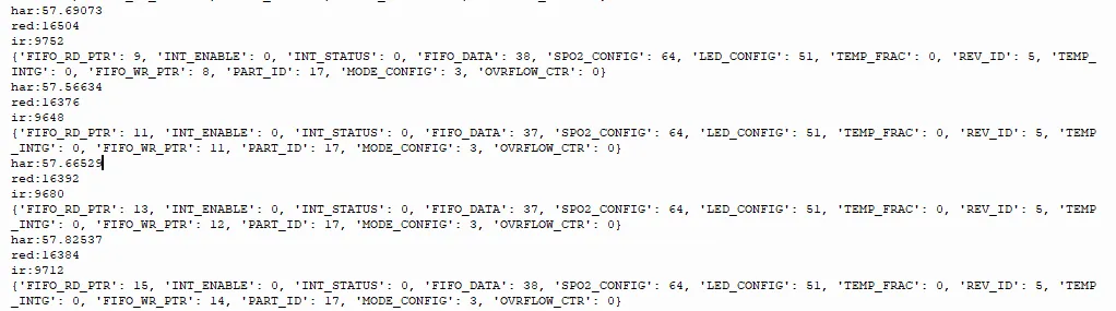
As you can see, the routine can run properly and outputs RED, IR, and HAR; after sufficient data is collected, the blood oxygen value and register value will be output.
4. Drivers
max30100_driver.rar 9 KB
5. BOM & Recommended Alternative Parts
None.
VI. Revision History
Document Version | Date of Modification | Modifier | Revised Content |
v1.0 | 2025-11-22 | Li Zisheng | Initialize Document |
v1.1 | 2026-02-12 | Xin Ruili | Create an open version of the document based on the internal document version v1.0. |
v1.2 | 2026-03-29 | Xin Ruili | Modified the application experiment section |
VII. Relevant Materials
7.1 Chip Datasheet
C92512_Heart Rate Sensor_MAX30100EFD+_Datasheet_Heart Rate Sensor_MAX30100EFD+_English Datasheet.PDF 875 KB
7.2 Unique Icons for PCB Silk Screen