Contents
- I. Module Introduction
- II. Introduction to Major Chips
- 2.1 Chip Overview
- 2.2 Pin Definition
- 2.3 Functional Block Diagram
- 2.4 Performance Parameters
- 2.5 Reference Circuit
- 2.6 Chip Configuration
- 2.7 Communication Interfaces and Related Protocols
- 2.8 PCB Routing Precautions
- III. Circuit Engineering
- 3.1 Circuit Source Engineering
- 3.2 Module Usage Instructions
- 3.3 Application Experiment
- IV. Drivers
- 5. BOM & Recommended Alternative Parts
- VI. Revision History
- VII. Relevant Materials
- 7.1 Chip Datasheet
- 7.2 PCB Silkscreen Specific Icons
I. Module Introduction
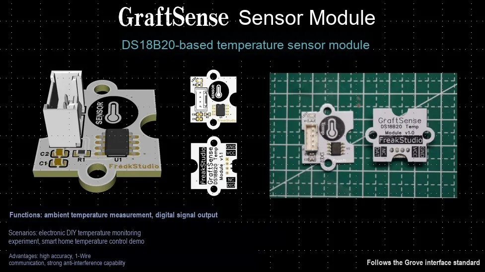
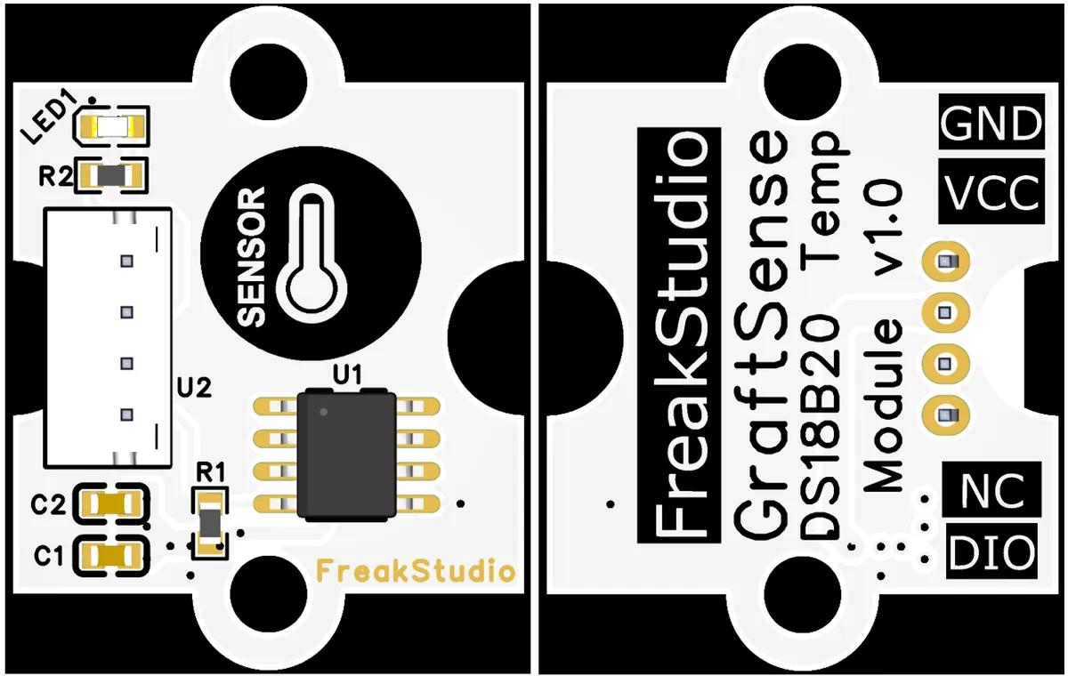
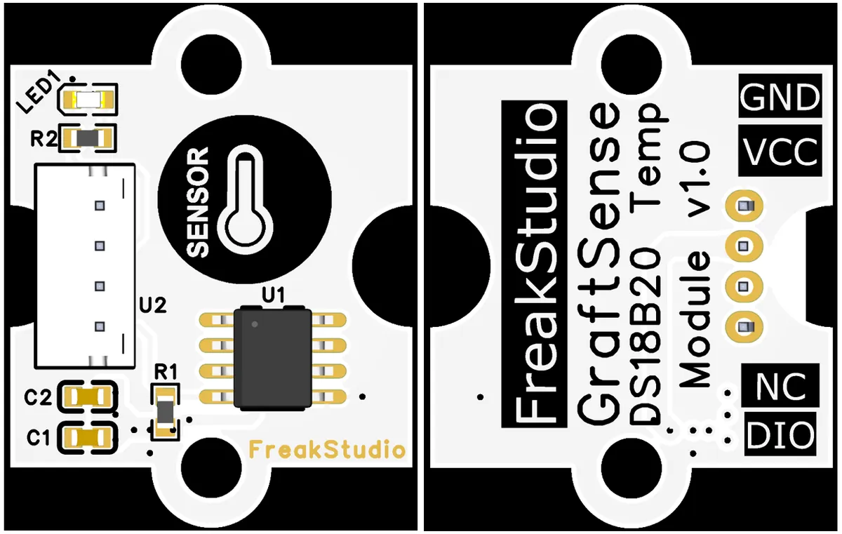
The temperature sensor module based on DS18B20 is a device that takes the DS18B20 chip as the core, equipped with a 4.7kΩ pull-up resistor, power filter capacitor and status indicator LED, adopts the 1-Wire (DIO) Communication Protocol, supports temperature measurement from -55℃ to + 125℃(default 12-bit resolution, accuracy of 0.0625℃), and can be quickly connected to the main control device through the GND, VCC, and DIO pins, which is suitable for scenarios such as environmental monitoring and home appliance temperature control.
II. Introduction to Major Chips
Here, in certain sections, we will take DS18B20 's domestic alternative chip MY18E20 as an example for introduction.
2.1 Chip Overview
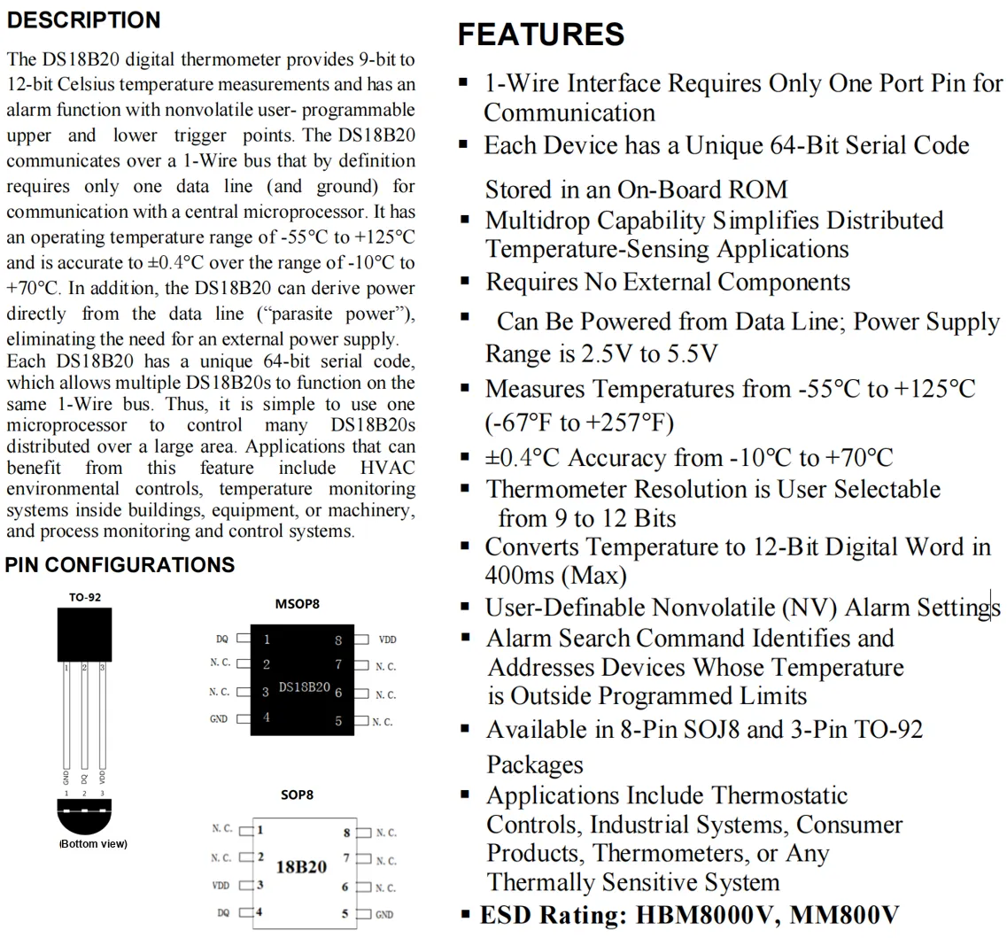
DS18B20 is a high-precision programmable digital single-bus temperature measurement chip:
- Its temperature measurement range is from -55°C to + 125°C, with a maximum resolution of 0.015°C
- The maximum deviation is ±0.5°C within the range of -10°C to + 85°C, and the maximum error at extreme operating temperatures is less than ±1.5°C.
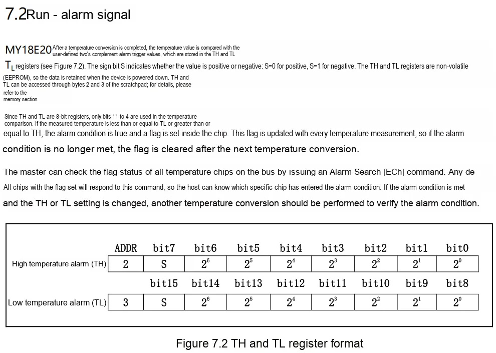
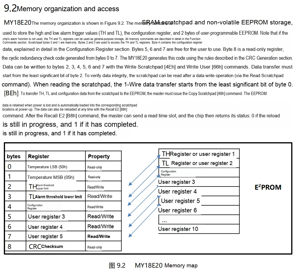
- The chip has a built-in 80-bit non-volatile memory cell for storing user-defined information, such as high and low temperature alarm thresholds, sensor node IDs, location information, temperature calibration data, etc.
A microprocessor can, via a GPIO port, read and write the chip's control registers per software instructions of the 1-Wire protocol to configure parameters such as temperature measurement accuracy and alarm thresholds, and periodically collect digital temperature data.
2.2 Pin Definition
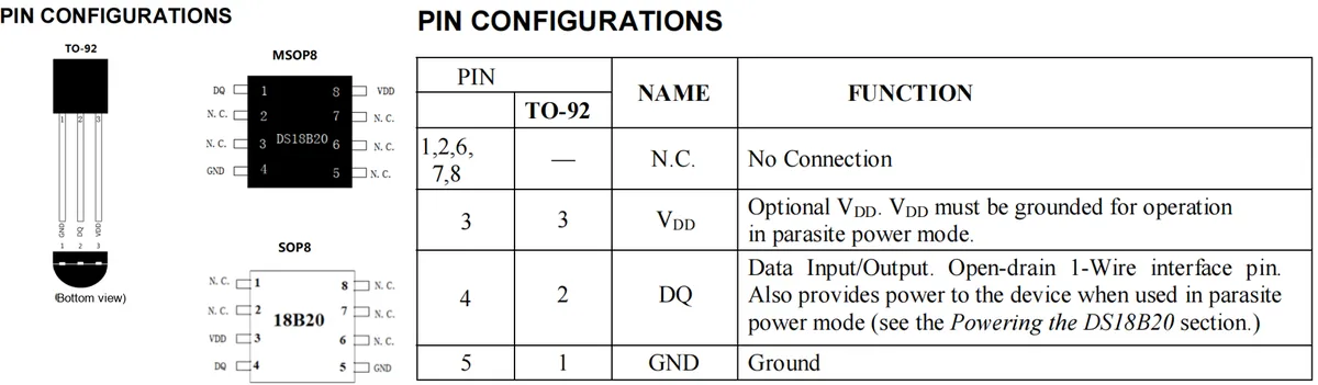
The DS18B20 is available in multiple packages including TO-92, MSOP8, and SOP8. The core functional pins and their definitions are as follows:
| Pin No. | Name | Function description |
| 1 | GND | Ground, provides the reference ground for the device. |
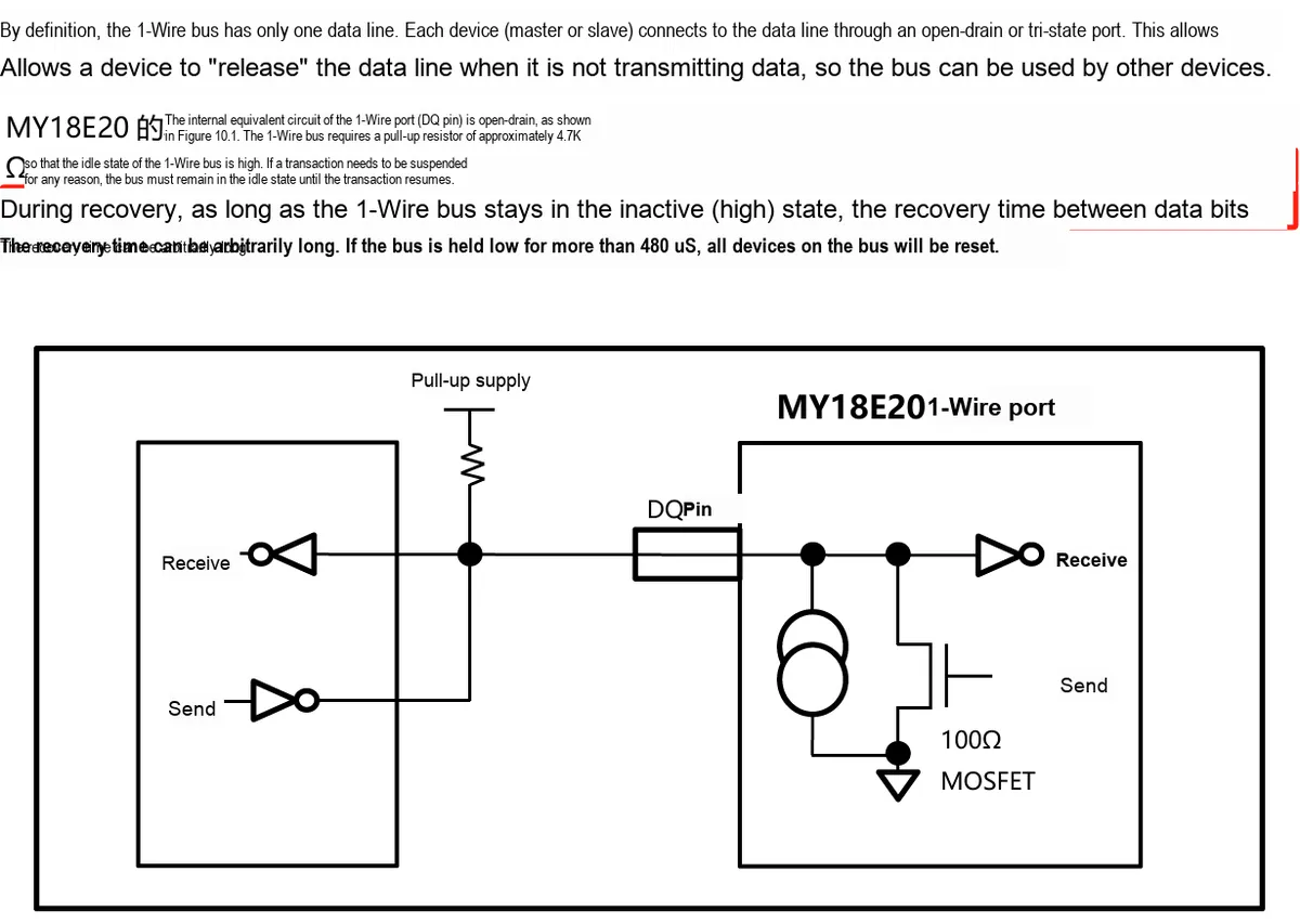
| 2 | DQ | Data Input/Output: uses an open-drain single-wire (1-Wire) interface; in parasitic power mode, this pin also supplies power to the device. |
| 3 | VDD | Optional VDD: connect a 3.0V~5.5V supply when externally powered; in parasitic power mode, VDD must be grounded. |
2.3 Functional Block Diagram
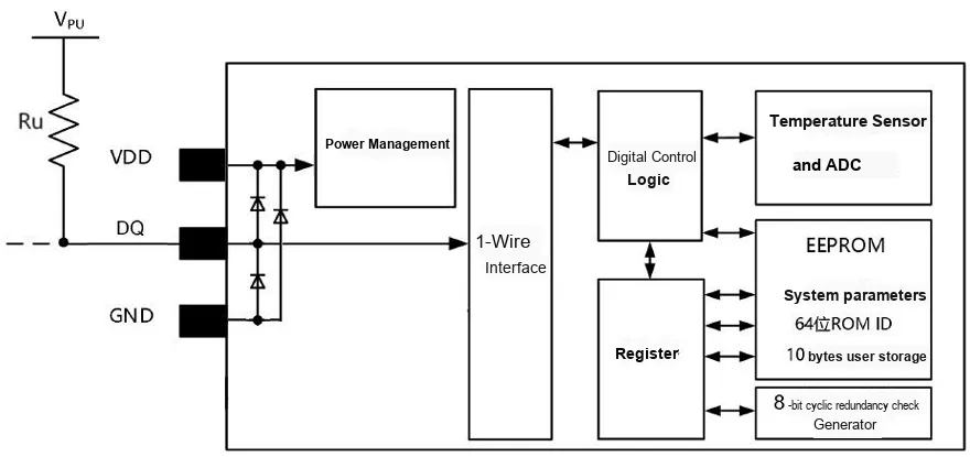
MY18E20 The sensor mainly consists of the following components:
- EEPROM: mainly stores system parameters, 64-bit
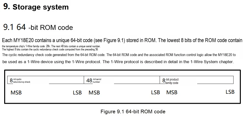
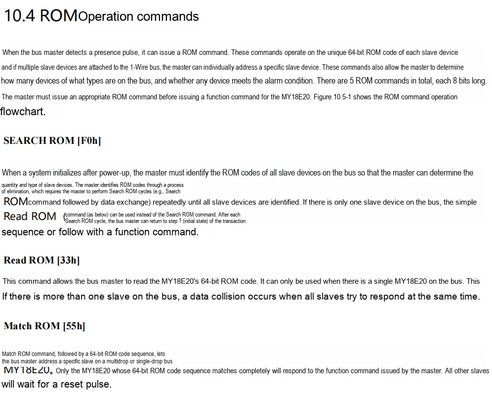
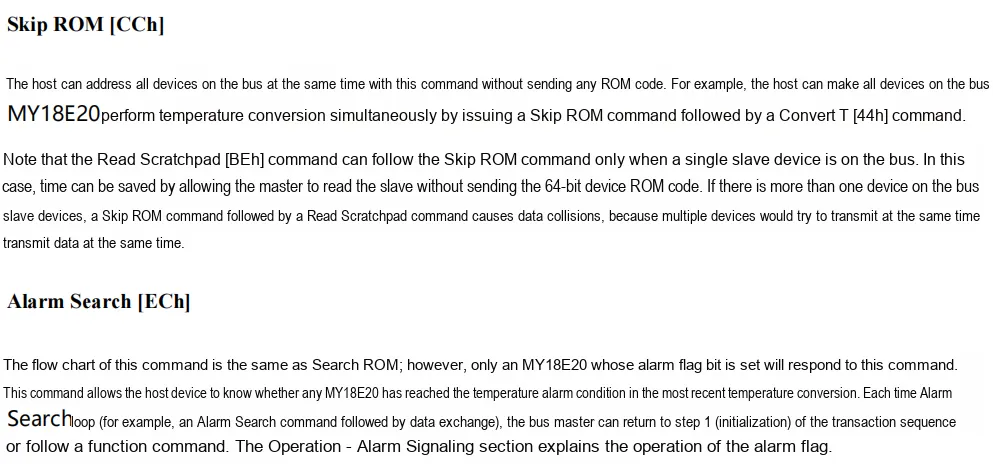
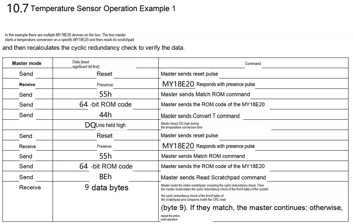
ROM IDand 10-byte user storage; the 64-bitROMstores the unique ID sequence code of the device.The single-chip microcomputer (master) identifies and addresses the devices on the bus via the unique 64-bit code of each device. Since every device is assigned a unique code, there is theoretically no upper limit to the number of devices that can be connected to the bus and addressed.
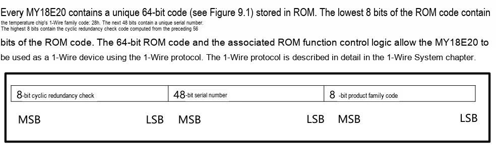
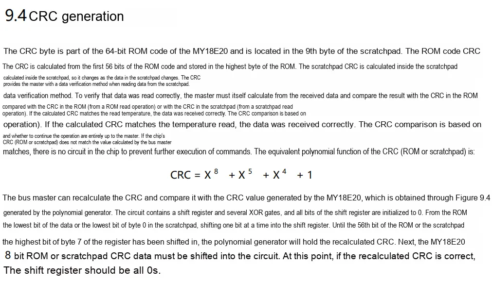
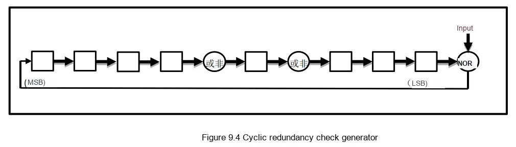
- 8-bit Cyclic Redundancy Check Generator: The Cyclic Redundancy Check byte is part of the 64-bit ROM code of the MY18E20, located in the 9th byte of the scratchpad. The ROM code Cyclic Redundancy Check is calculated from the first 56 bits of the ROM code and stored in the highest bits of the ROM. The Cyclic Redundancy Check code of the scratchpad is calculated inside the scratchpad, so it changes as the data in the scratchpad changes. The Cyclic Redundancy Check code provides the host with a data verification method when reading data from the scratchpad.To verify whether data is read correctly, the host must perform calculations on its own using the received data, and then compare the resulting value with the Cyclic Redundancy Check code stored in the ROM (from a ROM read operation) or the Cyclic Redundancy Check code stored in the scratchpad register (from a scratchpad read operation). If the calculated Cyclic Redundancy Check code matches the one that was read, the data has been received correctly and without errors.
- Temperature Sensor and ADC Unit: It performs temperature measurement and data conversion, and the generated temperature data is stored in the temperature register of the scratchpad.
- Numerical control logic: Perform corresponding operations based on the received ROM instructions and function instructions.
- Register: The register contains two bytes of temperature registers that store the digital output from the temperature sensor.
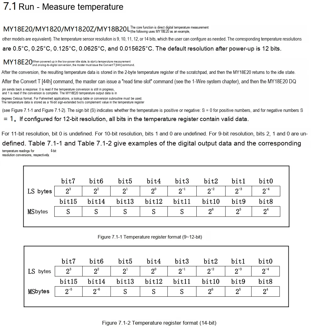
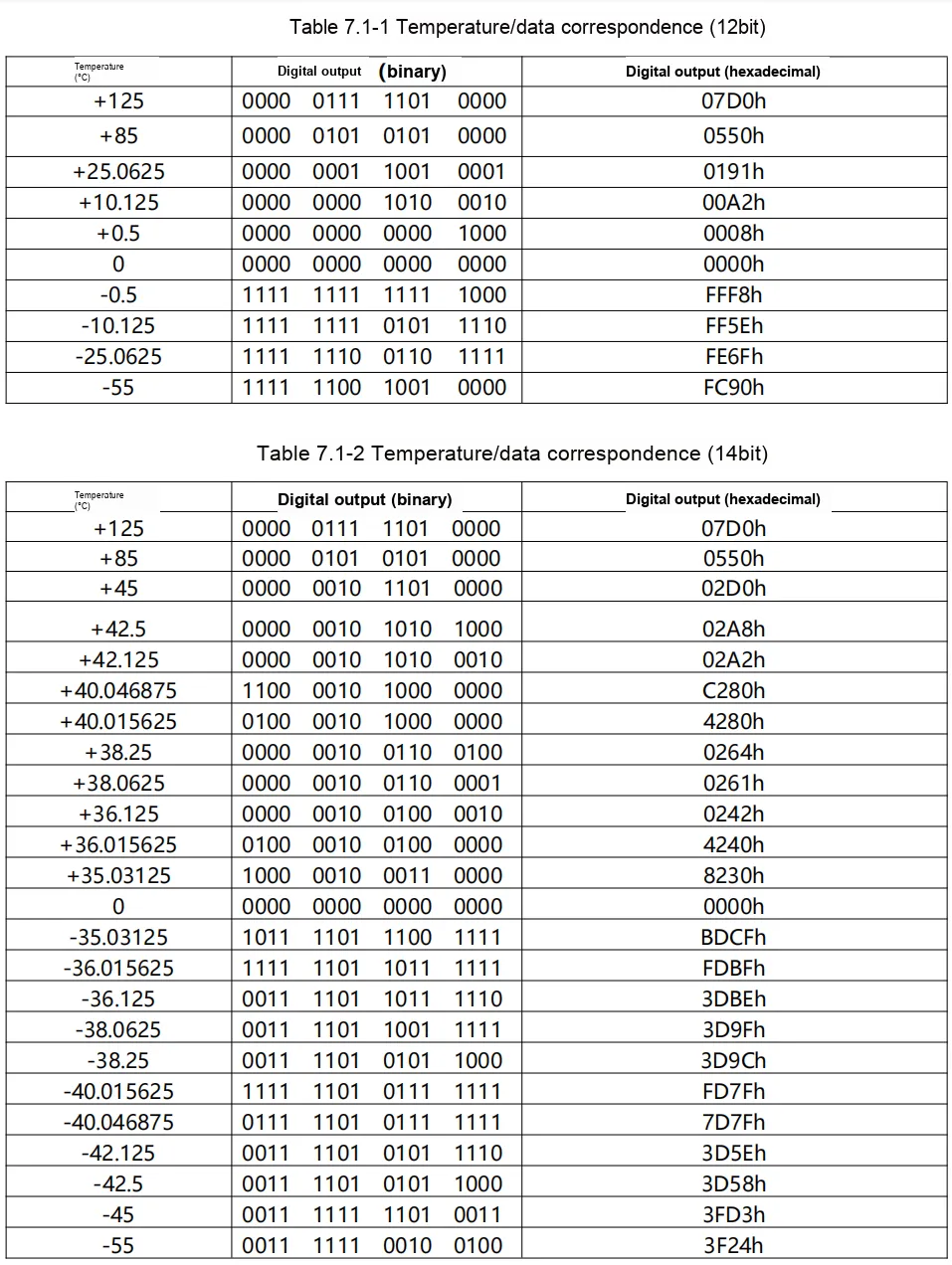
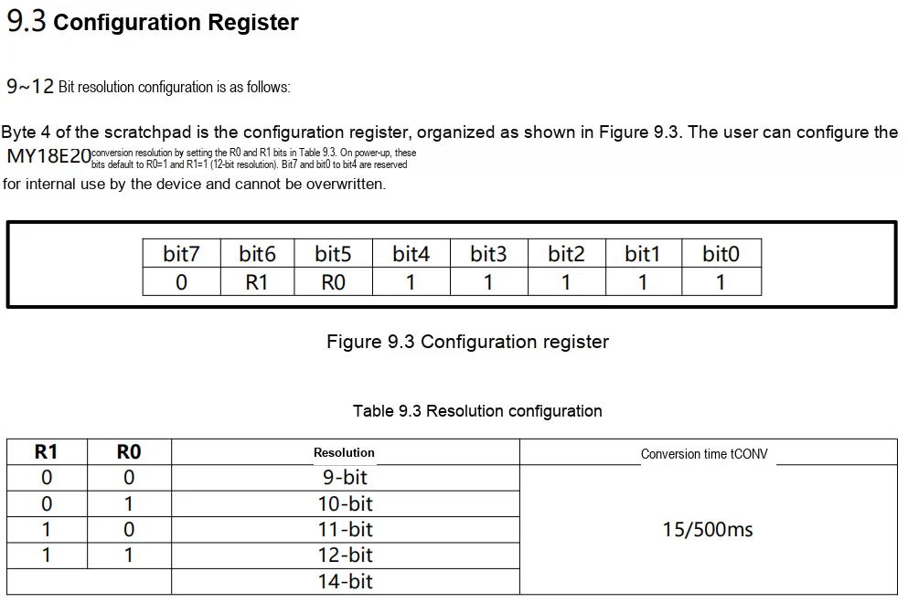
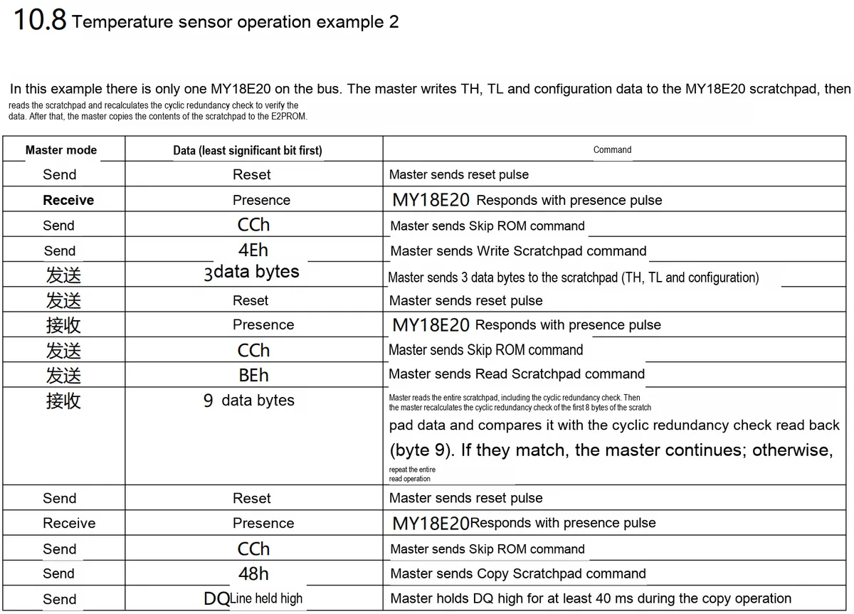
In addition, the register provides two alarm trigger threshold registers (TH and TL), one high and one low. The configuration register allows the user to set the resolution of temperature digital conversion to 9,10,11, or 12 bits (corresponding to temperature resolutions of 0.5°C, 0.25°C, 0.125°C, and 0.0625°C respectively, with the default being 12-bit resolution). An additional data space is provided for user use.
The configuration-related data in the register can be stored in the non-volatile EEPROM, so the data will not be lost when the chip is powered off; when the device is powered on next time, the configuration-related data in the EEPROM will be automatically written into the register.
- 1-Wire interface: converts the command data received by the 1-Wire interface and sends it to the digital control logic unit.
- Power Management: It converts the input voltage and distributes the power to each system for power supply.
2.4 Performance Parameters
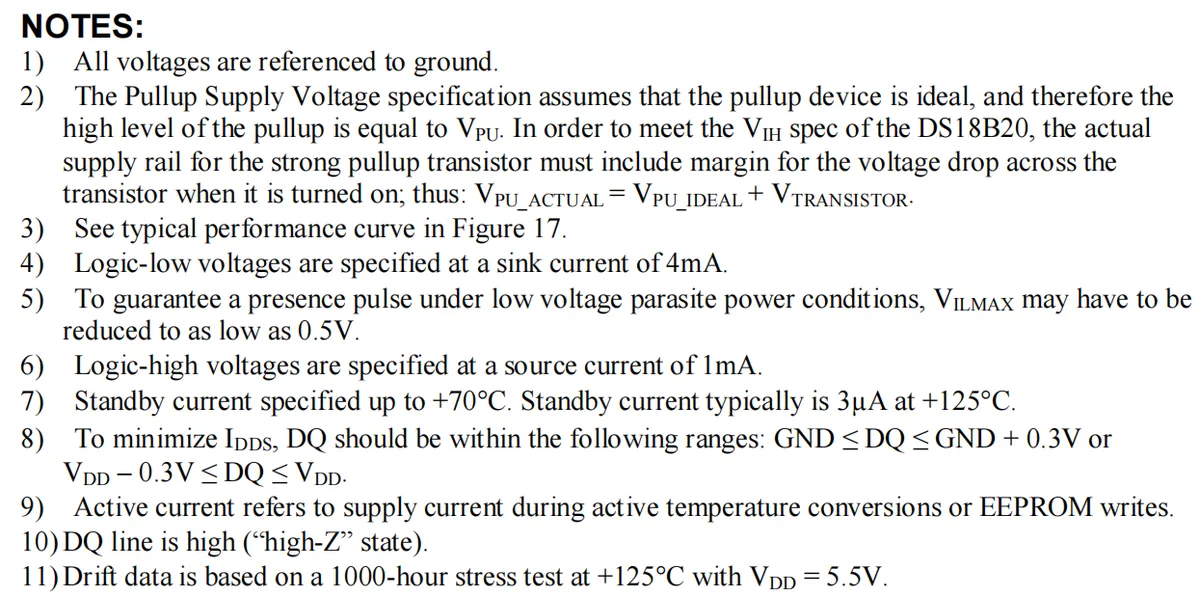
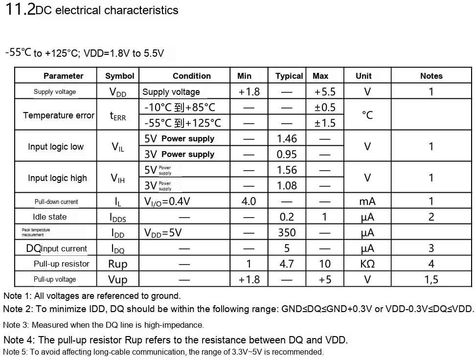
2.4.1 DC Electrical Parameters
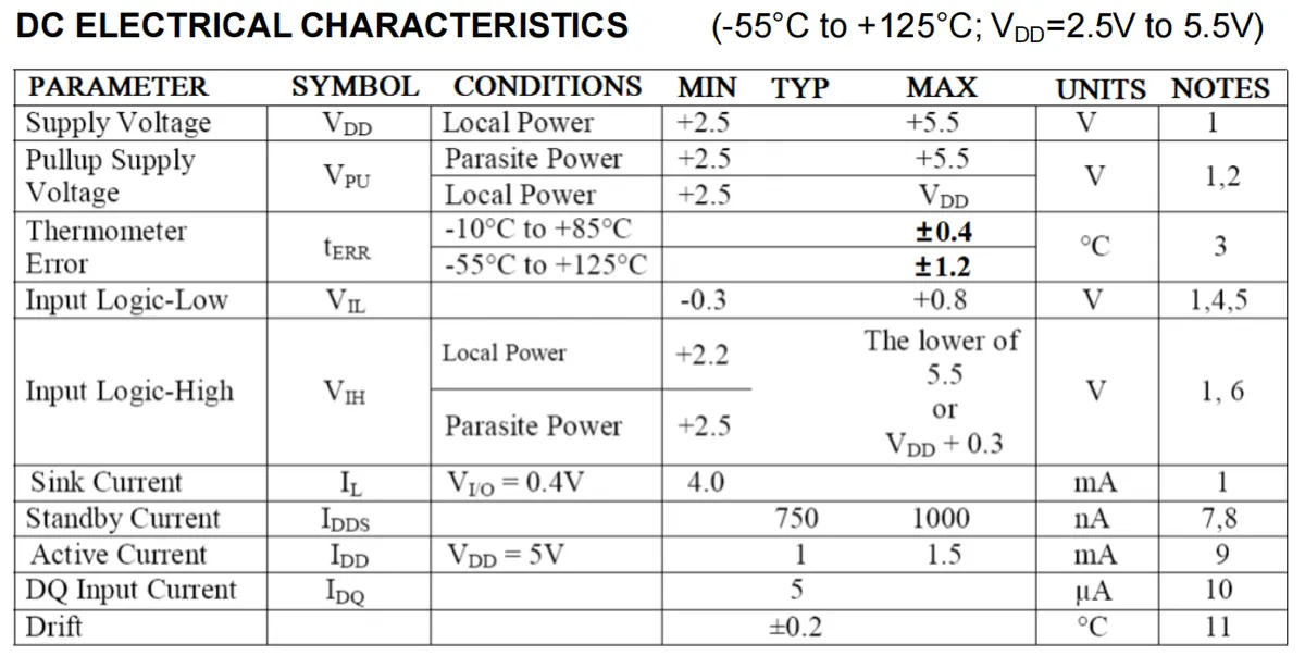
2.4.2 AC Electrical Parameters
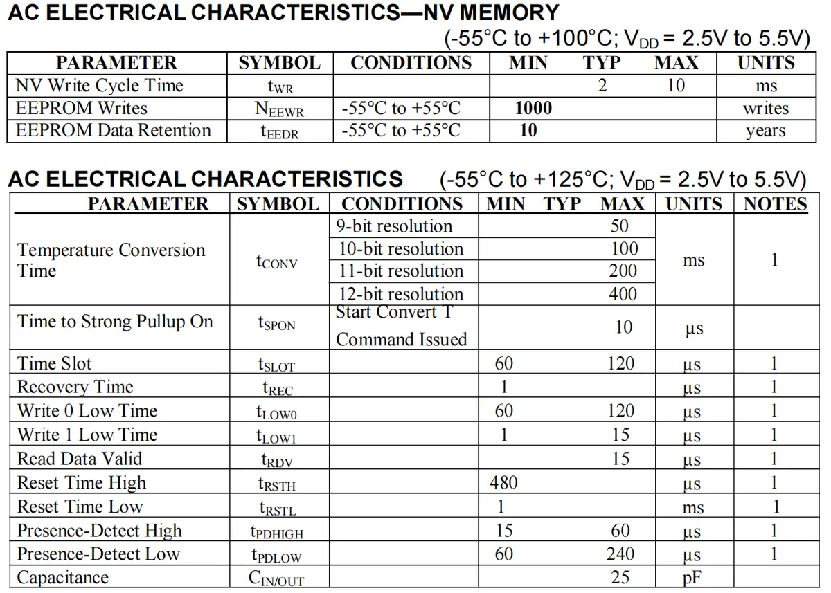
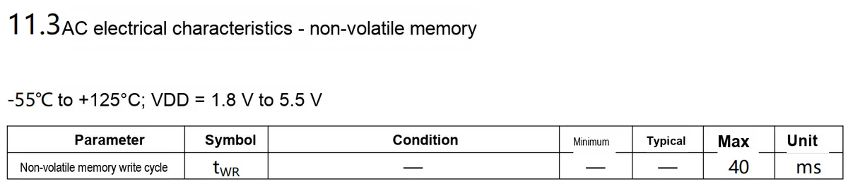
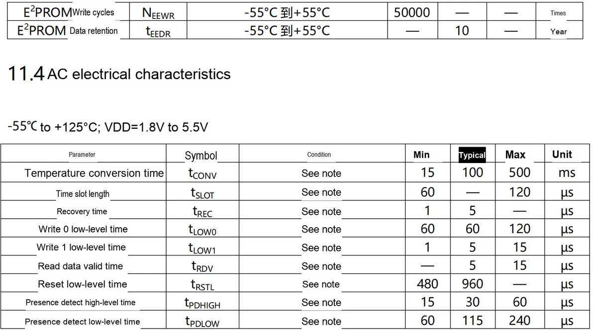
DS18B20 has two core components in its AC electrical parameters:
- Non-volatile (
NV) memory characteristics:- Write cycle time (
tWR): maximum 10ms, which determinesNVthe time overhead for data writing. EEPROMEndurance: At -55°C to + 55°C, it supports no fewer than 1000 write cycles, meeting the requirements for repeated configuration.- Data Retention Time (
tEEDR): At -55℃ to + 55℃, data can be stably stored for ≥10 years, ensuring the reliability of long-term storage.
- Write cycle time (
- Temperature Measurement and Timing Characteristics:
- Temperature conversion time (
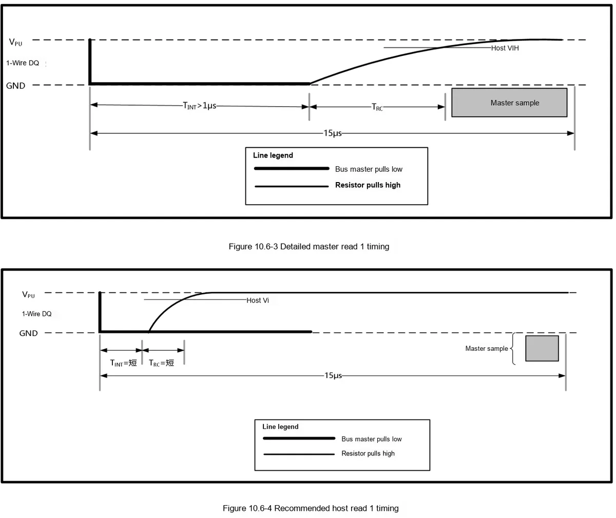
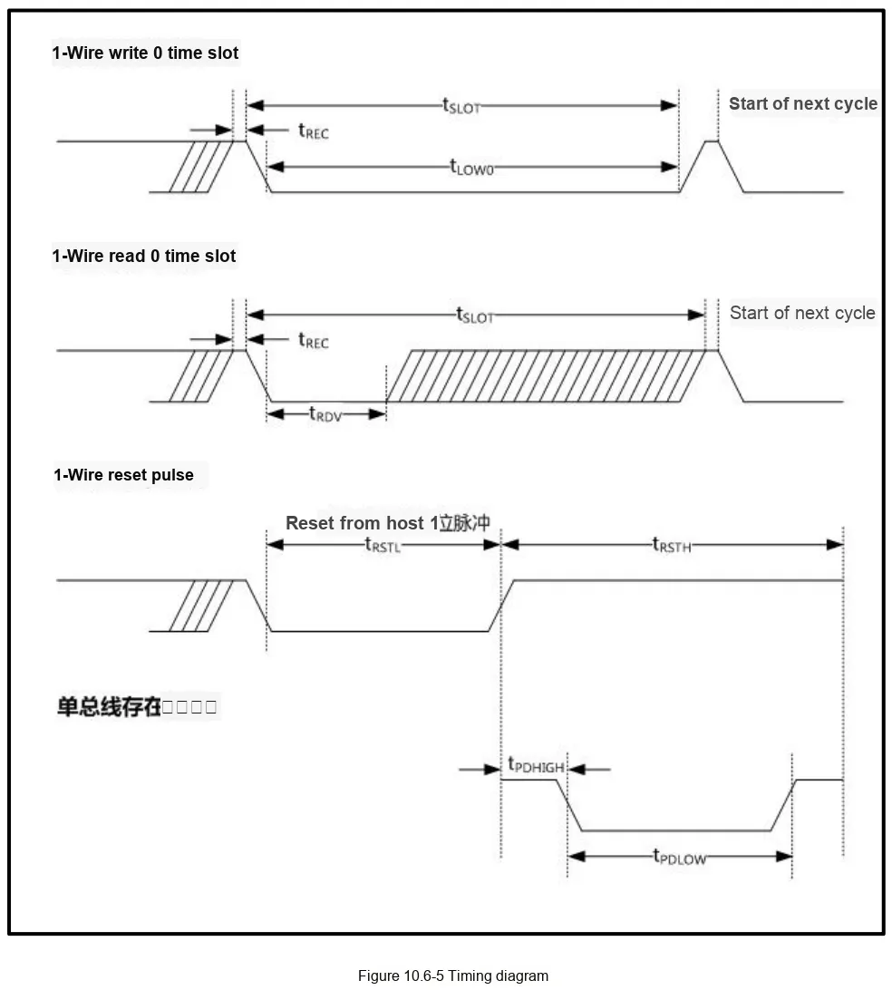
tCONV): increases as resolution improves (9-bit → 50ms, 12-bit → 400ms); at 12-bit resolution, the accuracy reaches the highest (0.0625℃) while the conversion speed is the slowest. - Single-bus timing: It involves strict time parameters for time slots, read/write operations, reset, etc. (for example, the low-level duration for writing a 0 needs to be 60~120μs, and the low-level duration for reset shall be no less than 1ms), which require precise matching to ensure reliable communication; the input/output capacitance (
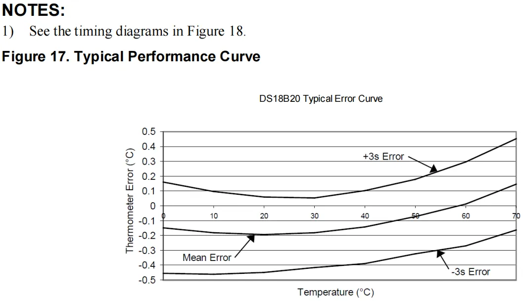
CIN/OUT) ≤25pF, which limits the number of devices that can be connected to the single bus. - Error characteristics: The measurement error fluctuates at different temperatures (as shown by the average error and the ±3σ error range in the figure), which assists in evaluating the temperature measurement accuracy across the full temperature range.
- Temperature conversion time (
2.4.3 Absolute Parameters
2.5 Reference Circuit

2.6 Chip Configuration
None.
2.7 Communication Interfaces and Related Protocols
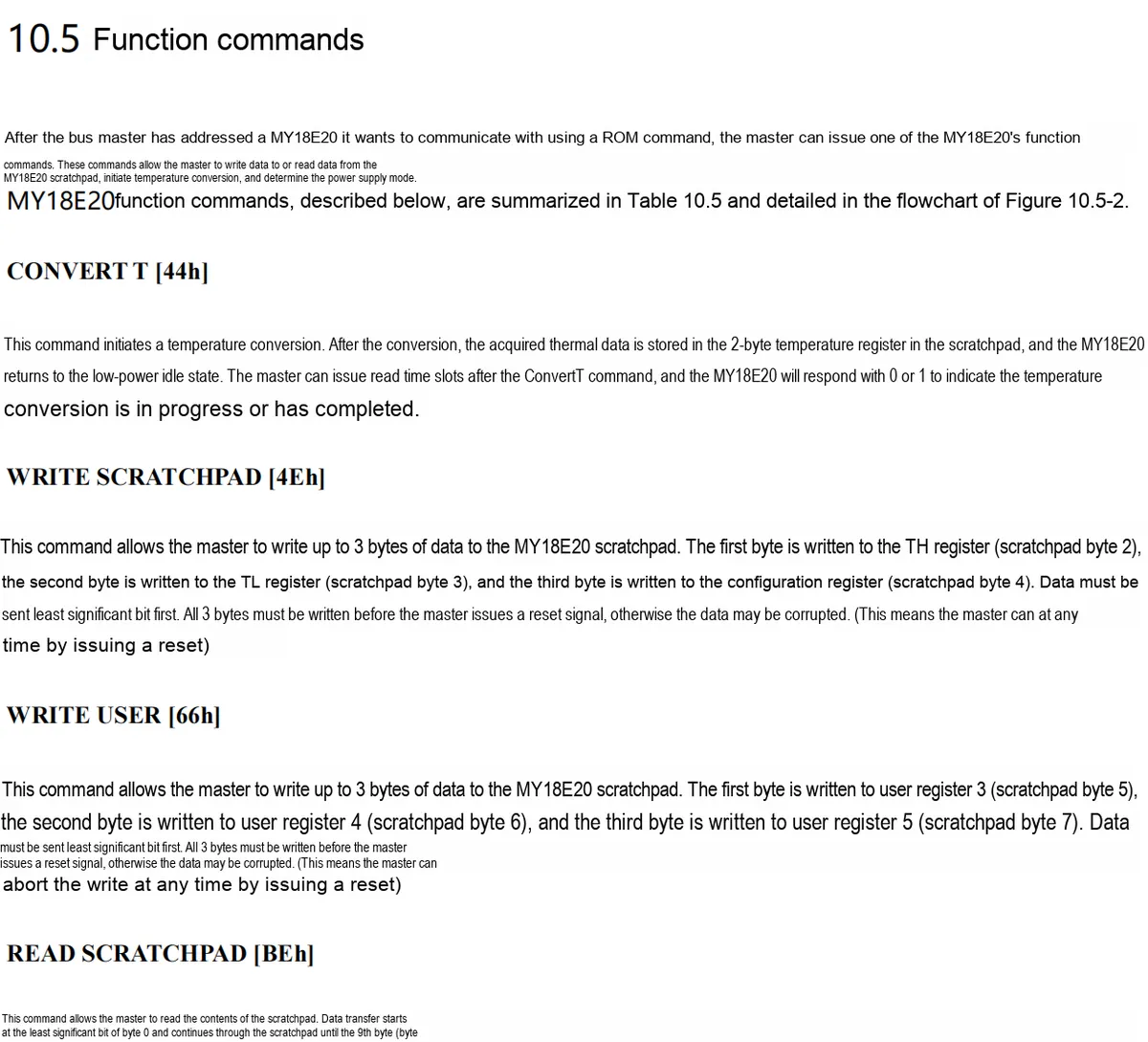
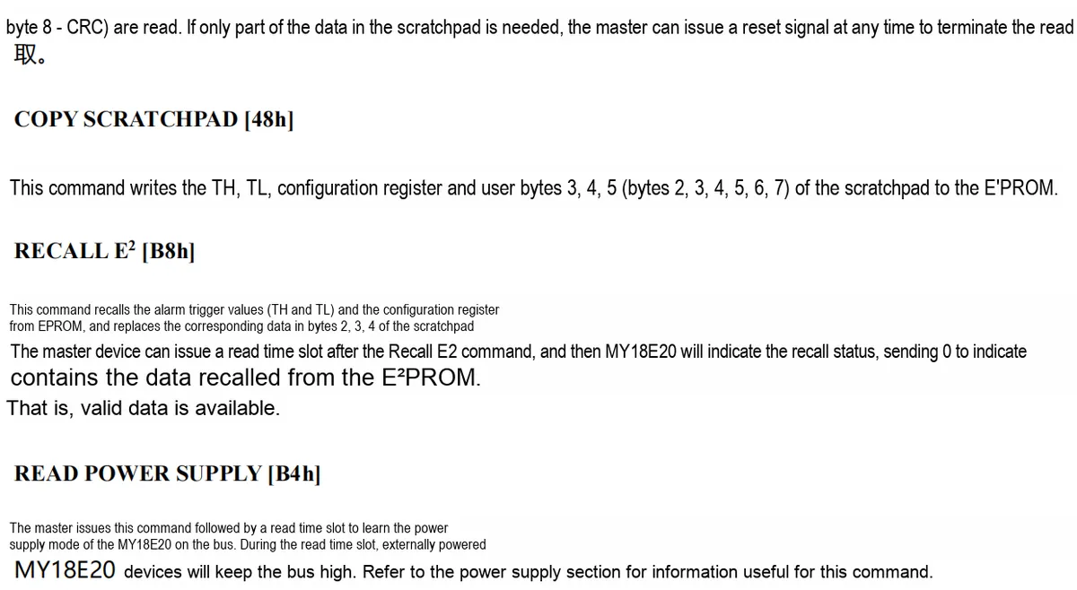
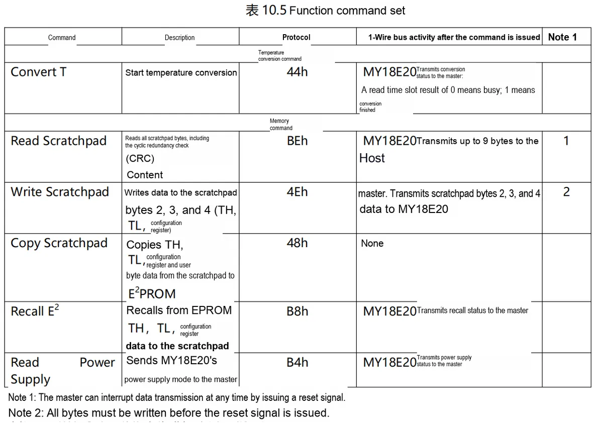
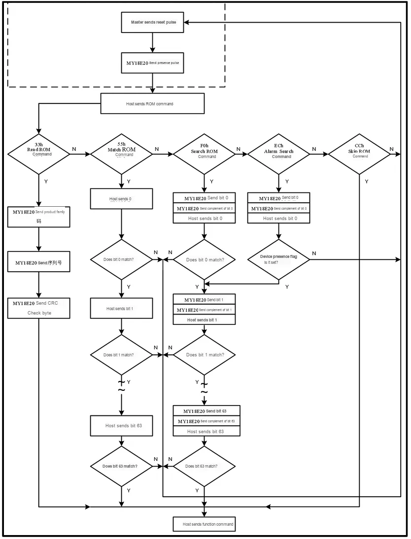
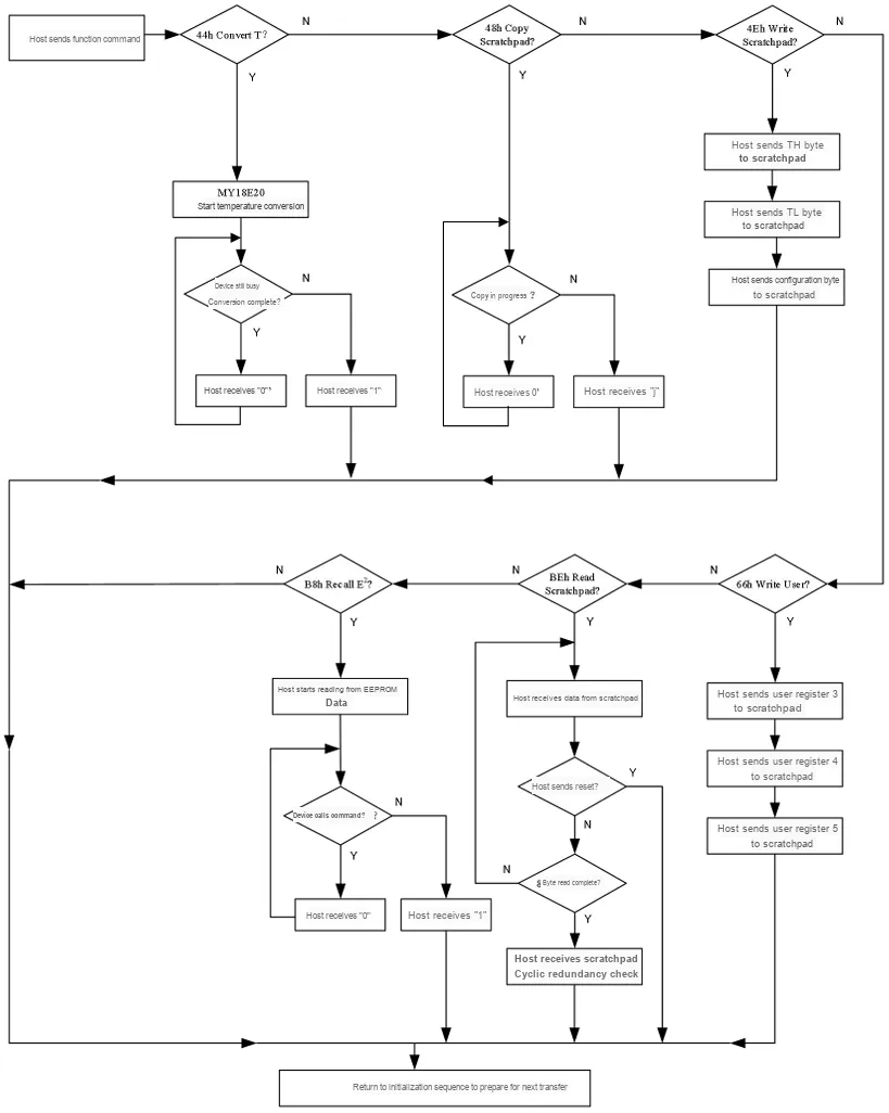
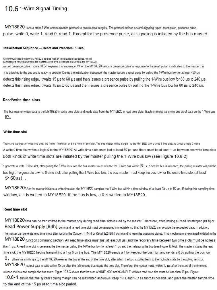
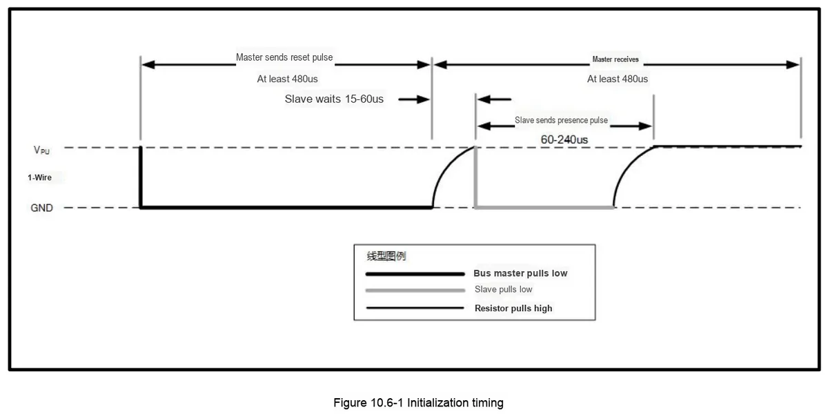
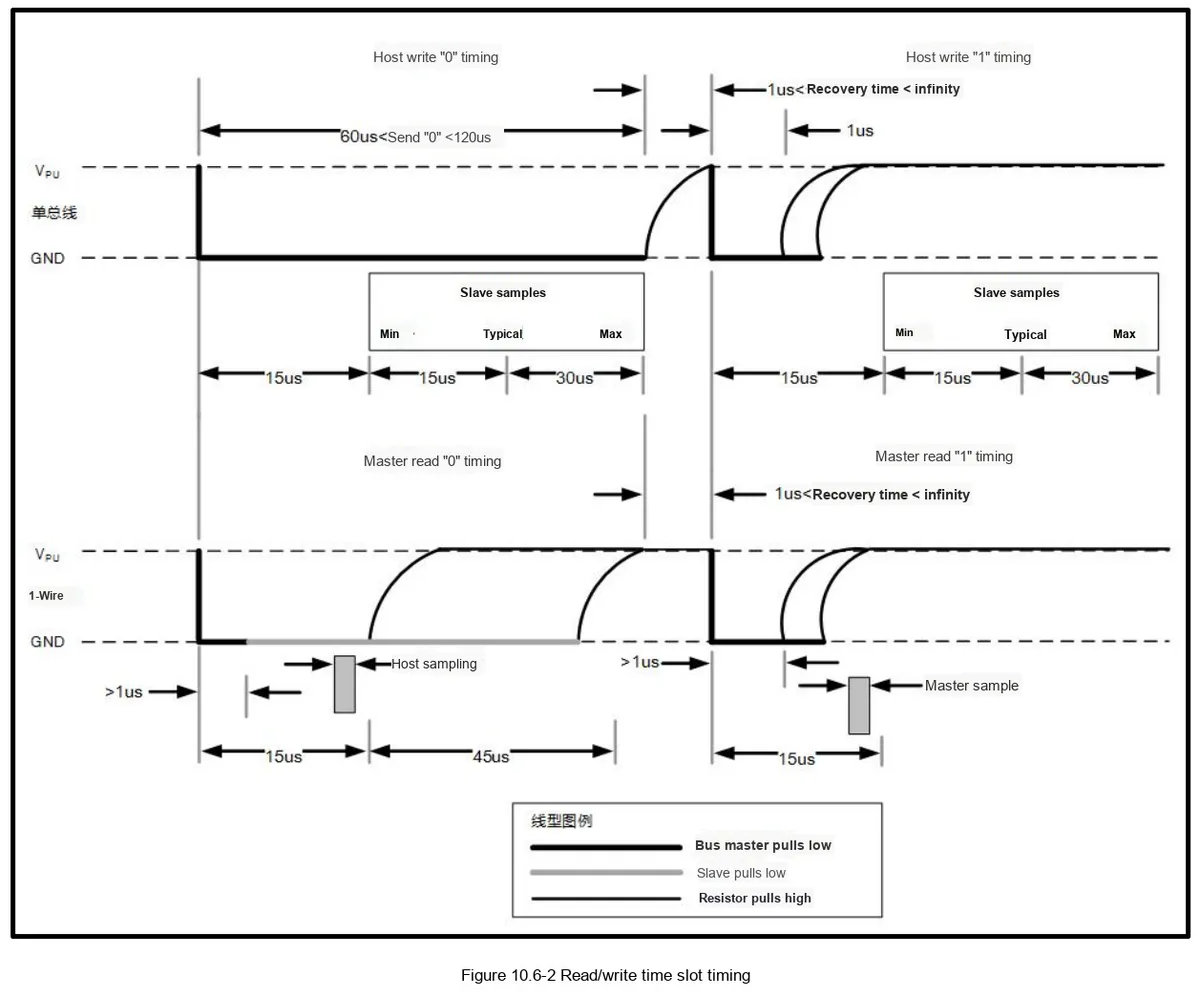
2.8 PCB Routing Precautions
None.
III. Circuit Engineering
3.1 Circuit Source Engineering
To obtain the source project of the circuit, please follow the official account [Freak Embedded]
3.2 Module Usage Instructions
The schematic diagram of this module is shown below:
SCH_Temperature Sensor Module Based on DS18B20_v1.0_2025-10-13.pdf 1.7 MB
This module adopts a single-bus communication interface DIO: a simplified Maxim (formerly Dallas)-defined Communication Protocol:
- Hardware Features: Only one data line (
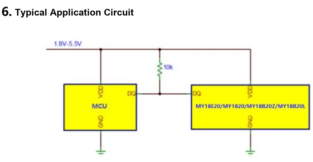
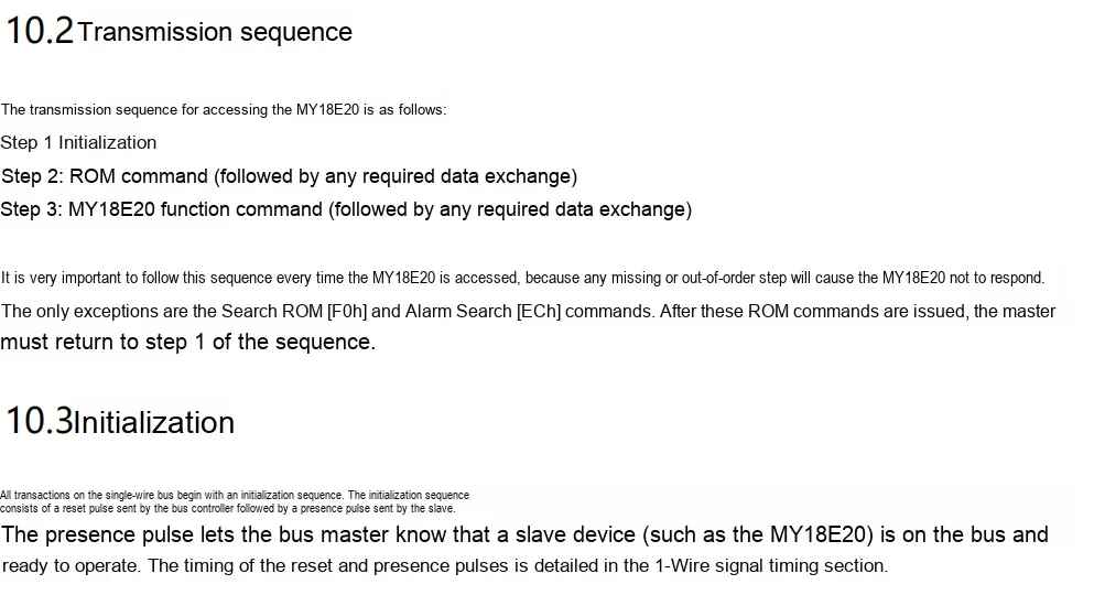
DIO) is required to realize bidirectional data transmission. TheDIOfeatures an open-drain output structure, which requires an external pull-up resistor of approximately 4.7kΩ connected to the power supply (such asVCC) to keep the bus at a high level when idle. - Communication logic: Data interaction is completed through strict timing control (such as reset pulses, read/write slots), and it supports multi-device bus sharing mounting (each device has a unique 64-bit
ROMaddress, which can distinguish multiple sensors on the bus). - Typical Scenario: Suitable for
DS18B20and similar temperature sensors in "multi-point temperature measurement" applications. While wiring is simplified, the software needs to accurately match the timing requirements of the 1-Wire bus (such as the time parameters for temperature conversion, data read and write) to ensure reliable communication.
3.3 Application Experiment
Here, we use the GraftPort-RP2040 development board for testing, and the temperature sensor module based on DS18B20 uses the DIO interface to communicate with the main controller.
Here, we first use the HY2.0-4P connection cable to connect the module to the GraftPort-RP2040 development board's DIO0 interface:
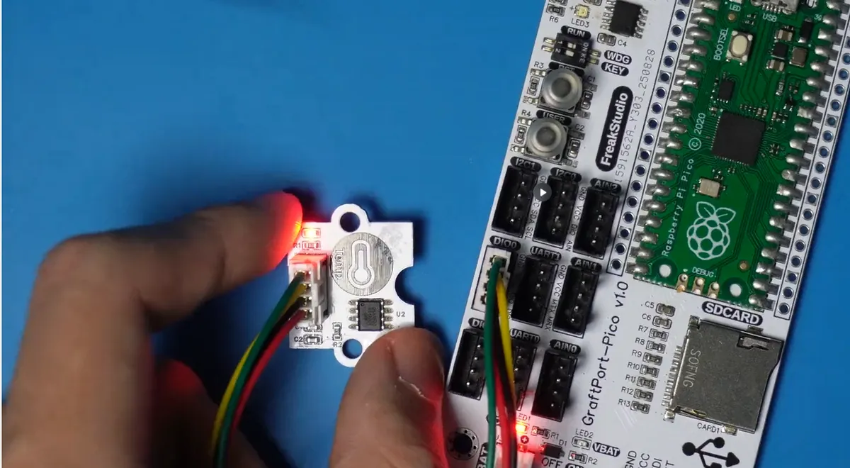
The module connections are shown in the following table:
Development Board Pins | Module Pins | Description |
Pin 6 |
| 1-Wire communication pin |
Pin 7 |
| - |
Here, we need to search for the relevant driver packages on uPyPI: https://upypi.net/zh/
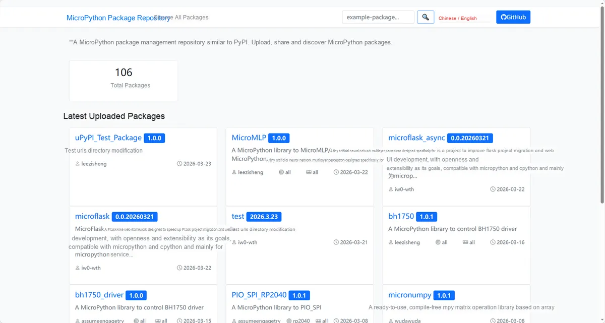
Enter ds18b20_driver to search, and the following will be displayed:
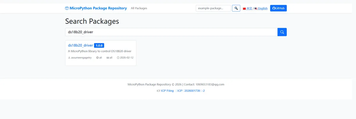
Click to copy the local installation command:
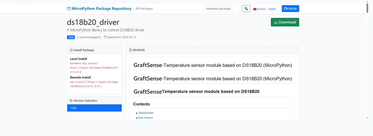
Here, we can use the mip tool to import module driver library code. Below are the usage commands for the mpremote tool:
mpremote mip install github:FreakStudioCN/GraftSense-Drivers-MicroPython/sensors/ds18b20_driverAfter importing the DS18x20 temperature sensor driver - MicroPython driver code, copy the following main.py code into our project:
# Python env   : MicroPython v1.23.0
# -*- coding: utf-8 -*-
# @Time    : 2024/7/22 3:01 PM
# @Author  : Li Qingshui
# @File    : main.py
# @Description : DS18B20 temperature experiment, using single-bus communication for data exchange

# ======================================== Import Modules ========================================

# Import hardware-related modules
from machine import Pin
# Import time-related modules
import time
# Import modules for single-bus communication
from onewire import OneWire
# Import the temperature sensor class
from ds18x20 import DS18X20

# ======================================== Global Variables ============================================

# ======================================== Functions ============================================

# ======================================== Custom Classes ============================================

# ======================================== Initialization ==========================================

# Delay to wait for the device to initialize
time.sleep(3)
# Print debug information
print('FreakStudio : Using OneWire to read DS18B20 temperature')

# Define the single-bus communication pin
ow_pin = OneWire(Pin(14))
# Define the temperature sensor
ds18x20 = DS18X20(ow_pin)

# ========================================  Main Program  ===========================================

# Scan for DS18B20 devices on the bus and get the list of device addresses
roms_list = ds18x20.scan()
# Print the list of device addresses
for rom in roms_list:
    print('ds18b20 sensor devices rom id:', rom)
# Have all DS18B20 devices on the bus convert the temperature
ds18x20.convert_temp()

# Read the temperature in a loop
while True:
    time.sleep_ms(500)
    for rom in roms_list:
        # Convert and print the temperature
        temp = ds18x20.read_temp(rom)
        # Print the temperature
        print('ds18b20 sensor {} devices temp {}'.format(rom, temp))
    # Start the temperature conversion
    ds18x20.convert_temp()
Burn the code, open a terminal, and use the mpremote tool to connect to the main controller; the output is as follows:
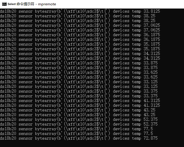
We can ignite a lighter and hold it close to the module, or cover the chip with our finger; at this point, we will observe that the temperature displayed by the module rises.
IV. Drivers
ds18b20_driver.zip 15 KB
5. BOM & Recommended Alternative Parts
None.
VI. Revision History
Document Version | Date of Revision | Modifier | Modified Content |
v1.0 | 2025-09-04 | ben0i0d | Initialize the document |
v1.1 | 2025-10-13 | Li Zisheng | Added Section 2.8 PCB Routing Notes Revised Section 3, Instructions for Circuit Source Engineering and Module Usage, and added a secondary heading: 3.1 Circuit Source Engineering, 3.2 Module Usage Instructions, 3.3 Application Experiments The BOM sheet has not been finally checked, the driver has not been re-verified, and the 3.3 application experiment Not yet specified. |
v1.2 | 2025-12-29 | Li Zisheng | Added application experiments and production files |
v1.3 | 2025-12-31 | Xin Ruili | Create an open version of the document based on the internal document version v1.2. |
v1.4 | 2026-03-29 | Xin Ruili | Modified the application experiment section |
VII. Relevant Materials
7.1 Chip Datasheet
C2843534_Temperature Sensor_MY18E20_Datasheet_WJ1187342.PDF 1.8 MB
DS18B20 Datasheet English Version.pdf 3.3 MB
7.2 PCB Silkscreen Specific Icons