Contents
- I. Module Introduction
- II. Introduction to Main Chips
- 2.1 Chip Overview
- 2.2 Pin Definition
- 2.3 Functional Block Diagram
- 2.4 Performance Parameters
- 2.5 Reference Circuit
- 2.6 Chip Configuration
- 2.7 Communication Interfaces and Related Protocols
- 2.8 PCB Routing Notes
- III. Circuit Engineering
- 3.1 Circuit Source Engineering
- 3.2 Module Usage Instructions
- 3.3 Application Experiment
- IV. Drivers
- 5. BOM & Recommended Alternative Parts
- 6. Revision History
- VII. Relevant Materials
- 7.1 Chip Datasheet
- 7.2 Unique Icons for PCB Silk Screen
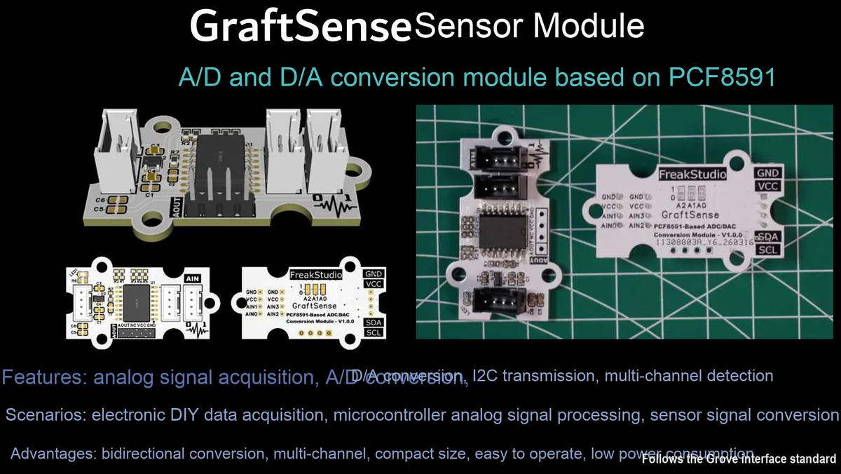
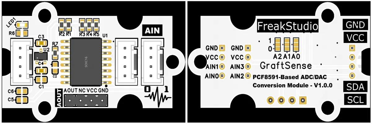
I. Module Introduction
PCF8591-based analog-to-digital and digital-to-analog conversion module that adopts an all-in-one chip solution of NXP PCF8591 8-bit high-precision ADC + DAC, integrates 4 analog inputs and 1 analog output, supports I²C communication interface, and allows slave address configuration via A0 / A1 / A2 pins to realize multi-chip cascading;Equipped with a 5V to 3.3V LDO voltage regulator circuit and power filter circuit, it is compatible with 3.3V level, has an ADC conversion range of 0~3.3V, and its DAC output can realize analog voltage feedback. Featuring low operating current, it is suitable for scenarios such as low-power sensor monitoring, analog signal closed-loop control and maker DIY, providing convenient and efficient analog-to-digital/digital-to-analog bidirectional conversion capability for the system.
II. Introduction to Main Chips
PCF8591 is an NXP -launched 8-bit I²C interface ADC + DAC integrated chip, which integrates 4 analog inputs (configurable as single-ended / differential) and 1 analog output, supports a maximum I²C communication rate of 100kHz, allows slave address configuration via the A0 / A1/A2 pins, operates at a supply voltage of 2.5V~6V, and is suitable for low-power, low-cost analog signal acquisition and analog voltage output scenarios.
2.1 Chip Overview
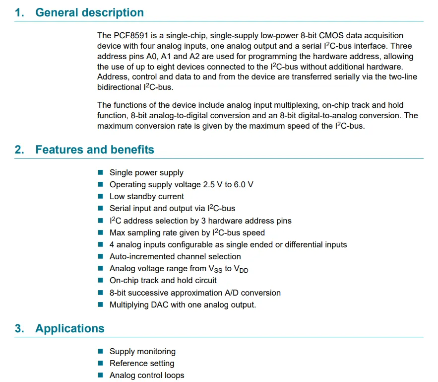
PCF8591 is an NXP -launched 8-bit low-power I²C interface ADC + DAC integrated chip, powered by a single supply of 2.5V~6V, it integrates 4 configurable analog inputs (single-ended/differential) and 1 analog output, with a built-in sample-and-hold circuit; 8 types of A0 / A1 / A2 pin-configurable I²C slave addresses are supported, its maximum sampling rate is determined by the I²C bus speed, and it is suitable for low-cost signal acquisition and output scenarios such as power supply monitoring and analog control.
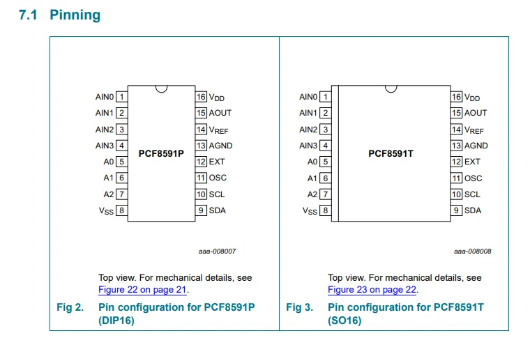
2.2 Pin Definition
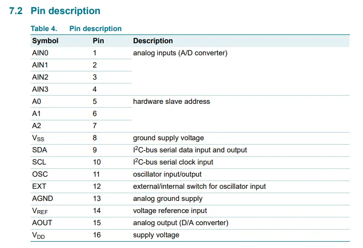
2.3 Functional Block Diagram
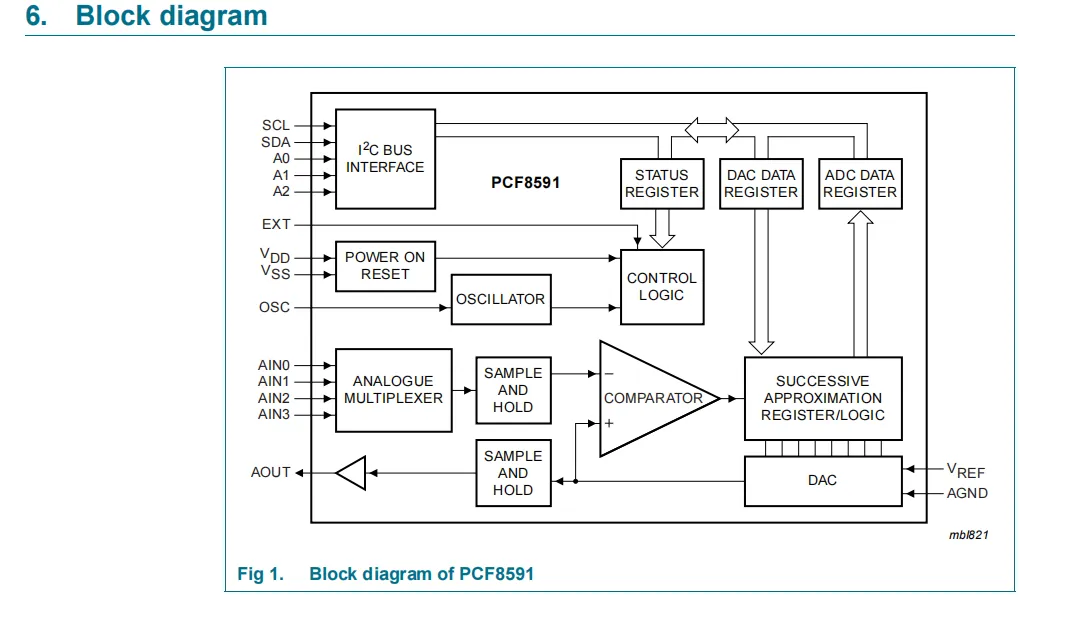
PCF8591 is an interface chip that integrates an 8-bit successive approximation ADC and a multiplying DAC with an I²C interface. Its 4 analog input channels are selected via an analog multiplexer and then sampled stably by a sample-and-hold circuit; analog-to-digital conversion is completed driven by the internal oscillator and reference voltage. Meanwhile, the DAC converts digital data into analog voltage and outputs it through the sample-and-hold circuit. It communicates with an I²C bus to connect with an MCU, and the A0 / A1 / A2 pins can configure the slave address to support multi-chip cascading, realizing low-power, low-cost bidirectional conversion between analog signal acquisition and analog voltage output.
2.4 Performance Parameters
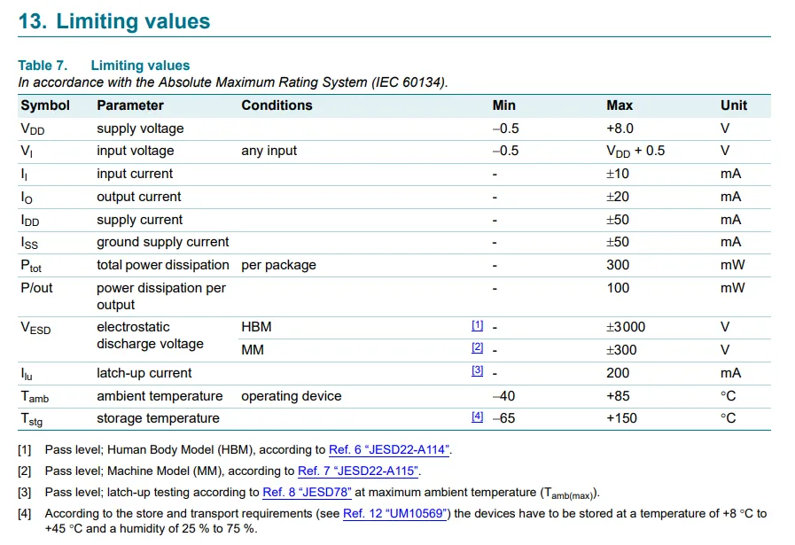
This is the limit parameter table of PCF8591 : the supply voltage range is -0.5V~ + 8.0V, the input voltage range is GND − 0.5V~ VDD + 0.5V, the input current is ± 10mA, the output current is ± 20mA, the total power consumption is ≤ 300mW, the ESD protection HBM mode is ± 3000V, the working temperature is -40 ℃~ + 85 ℃, the storage temperature is -65 ℃~ + 150 ℃, providing a safe and reliable stress boundary for chip design and application.
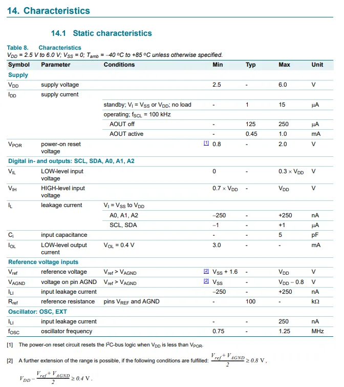
PCF8591 has the following static electrical characteristics: it operates on a single power supply of 2.5V to 6.0V, with a standby current of only 1μA and an operating current as low as 125μA, and is compatible with I²C digital levels (VIL ≤ 0.3 VDD, VIH ≥ 0.7 VDD). It features a built-in on-chip oscillator with a frequency ranging from 0.75MHz to 1.25MHz, and its reference voltage ranges from VSS + 1.6V to VDD, delivering stable and reliable electrical performance for low-power, low-cost analog-to-digital and digital-to-analog conversion.
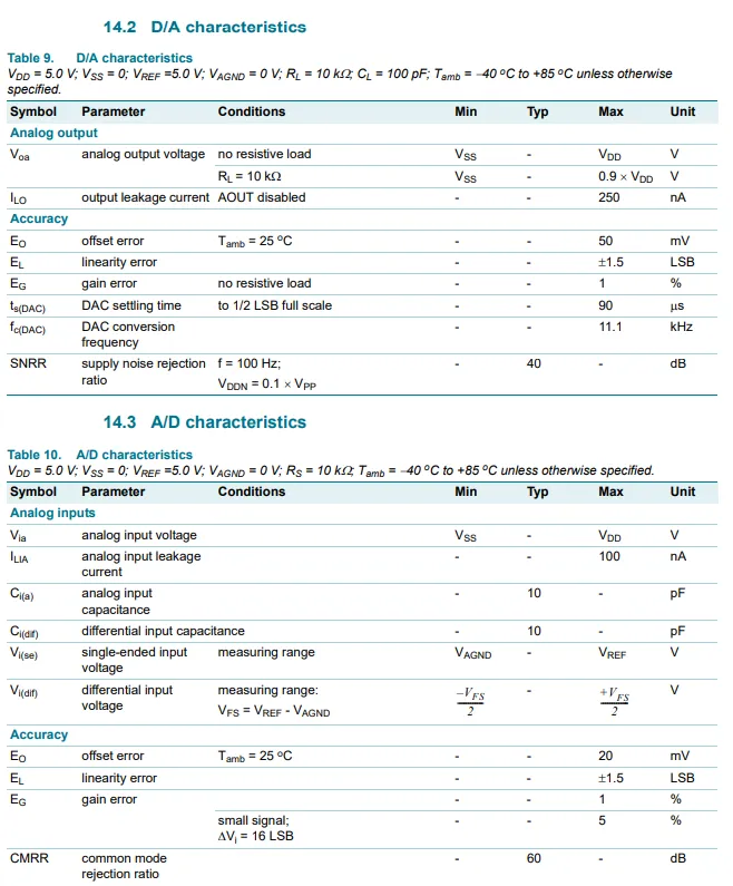
PCF8591 is an 8-bit ADC + DAC integrated chip. The DAC has an output range of 0 to VDD, a settling time of 90μs, and a conversion rate of 11.1kHz. The ADC supports single-ended/differential inputs, with a conversion range of 0 to VREF, an integral non-linearity of ±1.5LSB, and a common-mode rejection ratio of 60dB, making it suitable for low-cost, low-precision analog signal acquisition and output scenarios.
2.5 Reference Circuit
None.
2.6 Chip Configuration
None.
2.7 Communication Interfaces and Related Protocols
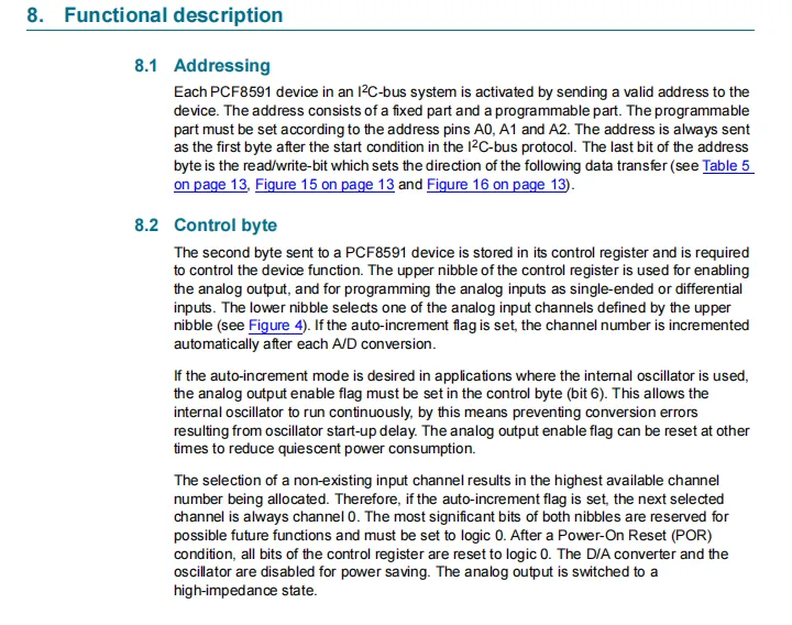
PCF8591 configures the A0 / A1 / A2 pin to set the I²C slave address; the second control byte is used to configure the analog input mode (single-ended / differential), channel selection and analog output enable, supports automatic channel increment function, the control register is cleared after power-on reset, and the DAC and oscillator are turned off to achieve low-power standby.
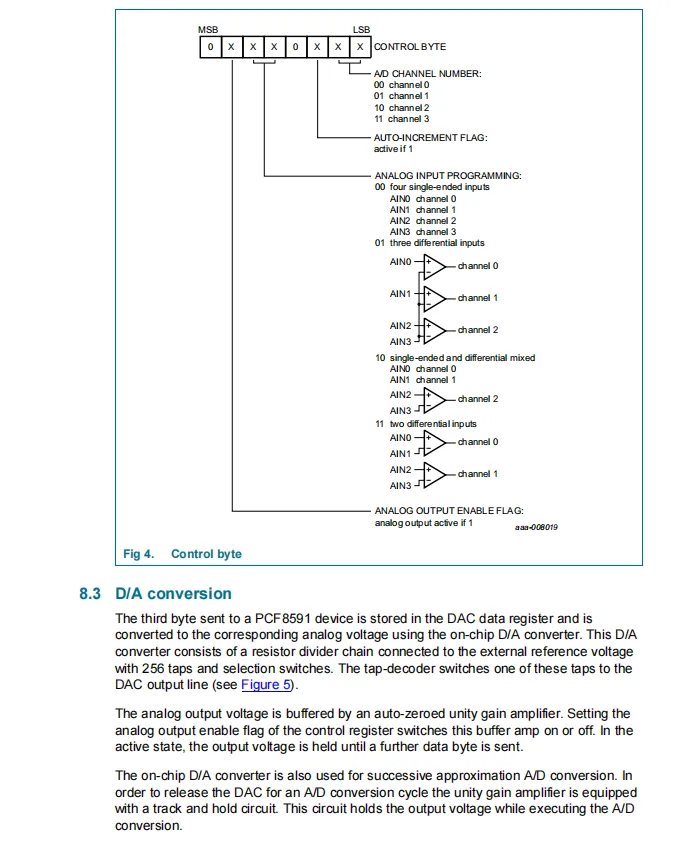
PCF8591 has a control byte that is used to configure the analog input mode (single-ended / differential), channel selection, auto-increment and analog output enable; meanwhile, it has a built-in 8-bit resistor-divider DAC which can convert digital data into analog voltage and output it via a buffer amplifier, and can also be reused as the core of ADC successive approximation conversion, thus realizing low-cost analog-to-digital / digital-to-analog bidirectional conversion.
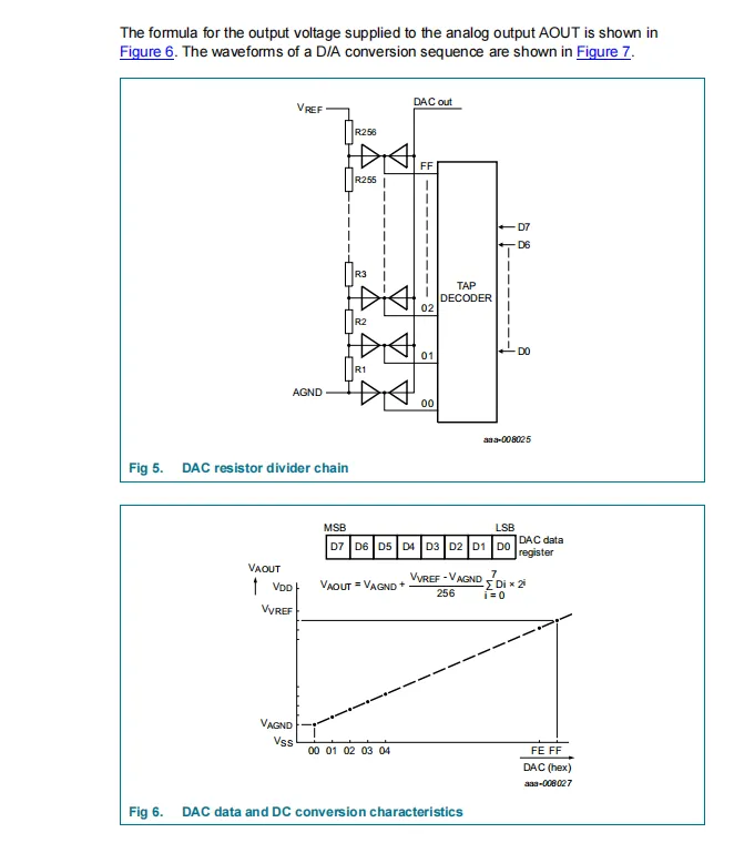
PCF8591 has a built-in 8-bit resistor-divider DAC, which realizes digital-to-analog conversion through a 256-stage resistor divider network. The output voltage formula is VAOUT = VAGND +(VREF − VAGND) × DAC_DATA / 256. The output varies linearly with the input digital value, enabling analog voltage output in the range of 0 to VREF, providing support for low-cost analog control and signal feedback.
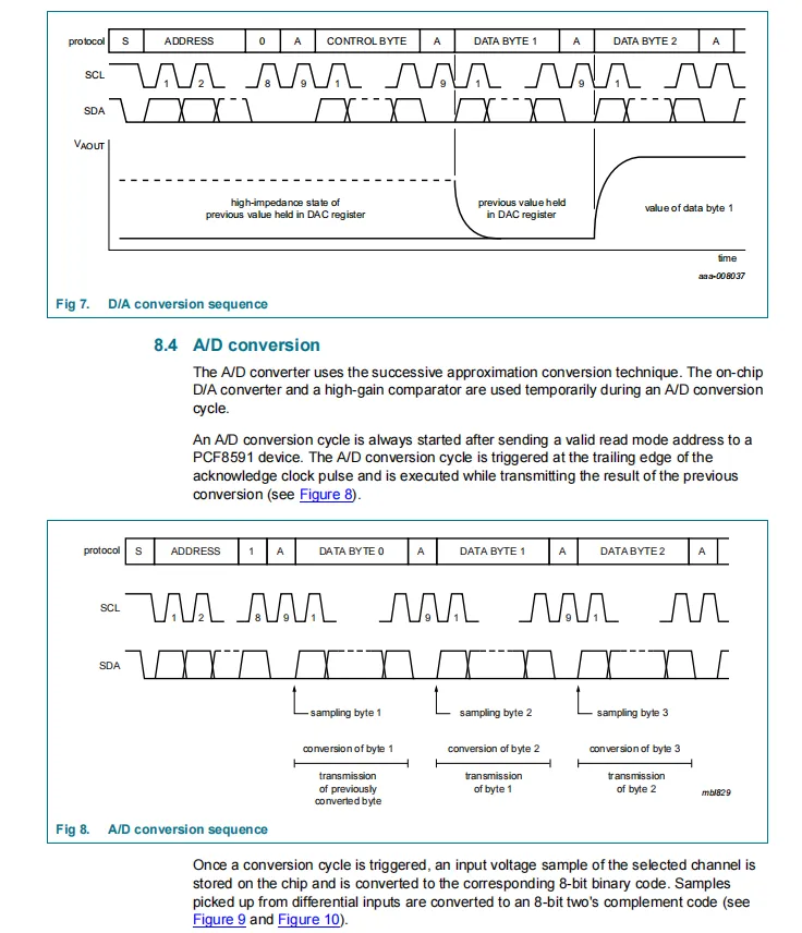
I²C communication timing: DAC conversion requires sending the address and control byte first, then writing the data byte to update the output voltage;ADC conversion adopts a successive approximation architecture. During a read operation, the address and read command are sent first, the chip triggers conversion on the acknowledge clock edge, and outputs the result of the previous conversion during transmission. It supports automatic channel increment reading to realize efficient analog-to-digital/digital-to-analog conversion timing interaction.
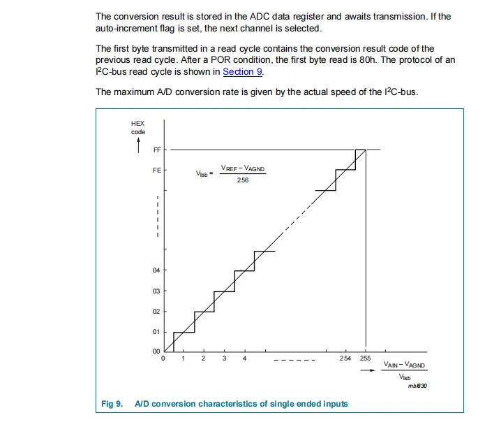
PCF8591 has a single-ended ADC conversion characteristic of 8-bit successive approximation, where the full-scale input voltage corresponds to a digital output of 0 to 255; the LSB voltage is determined by the reference voltage VREF and the analog ground VAGND, the conversion result features good linearity, the first read after power-on reset is a fixed value 0x80, the maximum conversion rate is determined by the I²C bus speed, and it is suitable for low-cost analog signal acquisition scenarios.
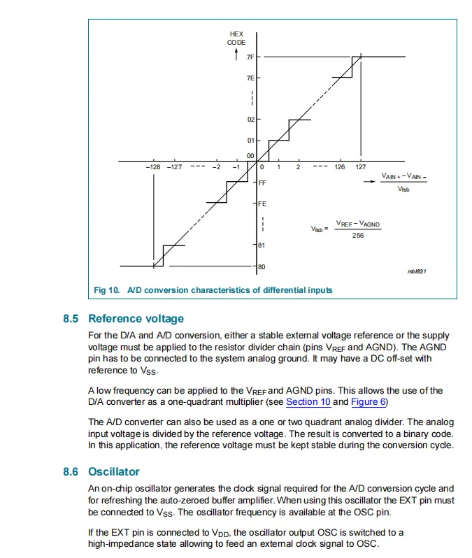
PCF8591 's differential ADC inputs adopt an 8-bit two' s complement format, with an output range of -128 to + 127, corresponding to an input voltage of ±2 VFS (VFS = VREF − VAGND). Meanwhile, this chip supports an external reference voltage and on-chip oscillator, and can also be connected to an external clock, providing support for high-precision differential signal acquisition and flexible clock configuration.
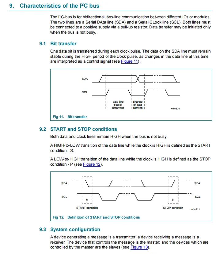
PCF8591 adopts a standard I²C two-wire open-drain interface. SCL / SDA require external pull-up resistors. It complies with the timing rule that SCL is at high level, and defines the SCL is at high level, and defines the START / STOP conditions by the high-to-low/low-to-high transition of SDA when SCL is at high level. It only acts as a slave to communicate with the master, realizing stable and reliable multi-device data interaction.
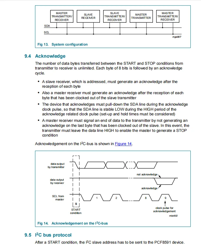
PCF8591 / I²C bus protocol, initiates and terminates transmission via START / STOP conditions, with an ACK response following each byte; the slave address is configured by the A0 / A1 / A2 pins, it only communicates with the master as a slave, supports multi-device mounting, and realizes stable and efficient ADC / DAC data read-write and configuration interaction.
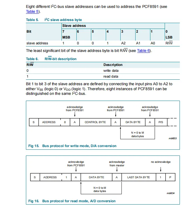
PCF8591 can be configured via the A0 / A1/A2 pins to support 8 types of I²C slave addresses (with a fixed prefix 1001 followed by the logic levels of A2 / A1 / A0). The last bit of the address serves as the read/write control bit (0 for write / 1 for read). During a write operation, the address, control byte and data byte are transmitted in sequence; during a read operation, the result of the last conversion is read. It supports multi-byte transmission, enabling flexible and efficient timing interaction for multi-device analog-to-digital / digital-to-analog conversion.
2.8 PCB Routing Notes
None.
III. Circuit Engineering
3.1 Circuit Source Engineering
To obtain the circuit source project, please follow the official account [Freak Embedded].
3.2 Module Usage Instructions
The schematic diagram of this module is shown below:
SCH_ADC and DAC Module Based on PCF8591_v1.0.0_2026-03-27.pdf 2.3 MB
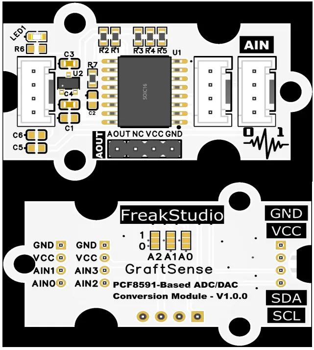
This module provides an IIC communication interface: it supports a standard I²C communication rate up to 100kHz, and can flexibly configure 8 types of A0 / A1 / A2 pin jumpers to configure 8 I²C slave addresses for multi-chip cascading; the SCL / SDA pins are equipped with pull-up resistors to comply with the I²C specification, are compatible with 3.3V level, and can stably transmit ADC configuration commands, 8-bit conversion data and DAC output data. Combined with the built-in programmable gain and differential input function, it realizes low-cost, low-power bidirectional conversion between analog signal acquisition and analog voltage output, which is suitable for scenarios such as sensor monitoring, analog control and maker DIY, and provides convenient and efficient analog-to-digital/digital-to-analog conversion interaction capability for the system.
Here, the AOUT interface is the DAC voltage output interface. Pin headers are not soldered by default, and you can solder them yourself when needed.
3.3 Application Experiment
Here, we use the GraftPort-RP2040 development board for testing, and the PCF8591-based analog-to-digital and digital-to-analog conversion module uses the I2C interface to communicate with the main controller.
Here, we first use the HY2.0-4P connection cable to connect the module to the GraftPort-RP2040 development board's I2C0 interface:
The module connections are shown in the following table:
Development Board Pins | Module Pins | Description |
Pin 4 |
|
|
Pin 5 |
|
|
|
|
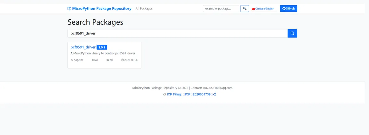
Here, we need to search for the relevant driver packages on uPyPI: https://upypi.net/zh/
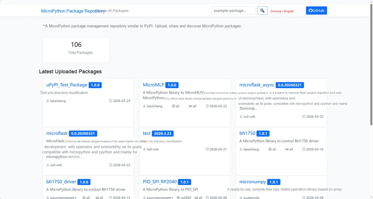
Enter pcf8591_driver to search, and the following will be displayed:
Click to copy the local installation command:
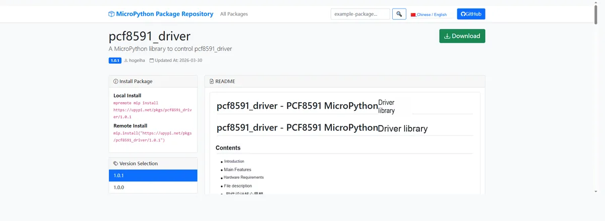
Import the module driver library code via the mip tool. Below are the usage commands for the mpremote tool:
mpremote mip install https://upypi.net/pkgs/pcf8591_driver/1.0.0Import the PCF8591-based ADC-DAC module - MicroPython driver code, then copy the following main.py code into our project:
# Python env   : MicroPython v1.23.0
# -*- coding: utf-8 -*-
# @Time    : 2026/3/13 8:00 PM
# @Author  : Developer
# @File    : main.py
# @Description : PCF8591 DAC/ADC test  Read analog channel voltage, output specified DAC voltage, Pico I2C communication

# ======================================== Import Modules =========================================

# Import the microsecond-level time module, used for I2C communication delays and program execution interval control
import time

# Import the I2C and Pin classes from the machine module, used for the hardware I2C interface and pin control
from machine import I2C, Pin

# Import the PCF8591 class, which encapsulates the core functions of the PCF8591 DAC/ADC chip
from pcf8591 import PCF8591

# ======================================== Global Variables ============================================

# Automatically identify the sensor address and define the global target address list
TARGET_PCF8591_ADDRS = [0x48, 0x49, 0x4A, 0x4B, 0x4C, 0x4D, 0x4E, 0x4F]

# Pico I2C controller ID (0 or 1)
I2C_ID = 0
# Pico SDA pin (recommended: 0/4/8/12/16/20)
I2C_SDA_PIN = 4
# Pico SCL pin (recommended: 1/5/9/13/17/21)
I2C_SCL_PIN = 5
# Reference voltage (the PCF8591 VCC voltage, usually 3.3V or 5V)
REF_VOLTAGE = 3.3
# I2C communication frequency (default 100kHz, compatible with PCF8591)
I2C_FREQ = 100000

# ======================================== Functions ============================================

# ======================================== Custom Classes ============================================

# ======================================== Initialization configuration ===========================================

time.sleep(3)
print("FreakStudio: PCF8591 ADC/DAC Test")
# Initialize the PCF8591 chip and catch exceptions during initialization
try:
    # I2C initialization (compatible with I2C/SoftI2C)
    i2c_bus = I2C(I2C_ID, sda=Pin(I2C_SDA_PIN), scl=Pin(I2C_SCL_PIN), freq=I2C_FREQ)

    # Start scanning for devices on the I2C bus
    devices_list: list[int] = i2c_bus.scan()
    print("START I2C SCANNER")

    # Check the I2C device scan result
    if len(devices_list) == 0:
        print("No i2c device !")
        raise SystemExit("I2C scan found no devices, program exited")
    else:
        print("i2c devices found:", len(devices_list))

    # Iterate over the address list to initialize the target sensor
    sensor = None  # Placeholder for the sensor object initialization
    for device in devices_list:
        if device in TARGET_PCF8591_ADDRS:
            print("I2c hexadecimal address:", hex(device))
            try:
                # Automatically identify and initialize the corresponding sensor
                sensor = PCF8591(address=device, i2c=i2c_bus)
                print("Sensor initialization successful")
                break
            except Exception as e:
                print(f"Sensor Initialization failed: {e}")
                continue
    else:
        # Target device not found, raise an exception
        raise Exception("No target sensor device found in I2C bus")

    # ========================================  Main Program  ============================================

    # -------------------------- Example 1: Read single-channel data --------------------------
    # Print the Example 1 title, indicating the single-channel analog value and voltage reading function
    print("\n=== Example 1: Read single channel analog value and voltage ===")
    # Read the analog value of channel AIN0 (0-255)
    analog_val = sensor.analog_read(PCF8591.AIN0)
    # Read the voltage of channel AIN0, calculated from the reference voltage
    voltage_val = sensor.voltage_read(PCF8591.AIN0, REF_VOLTAGE)
    # Print the analog value and voltage of channel AIN0 in formatted output
    print(f"AIN0 Analog Value: {analog_val} (0-255) | Voltage Value: {voltage_val:.2f} V")

    # -------------------------- Example 2: Read all channel data --------------------------
    # Print the Example 2 title, indicating the all-channel analog value reading function
    print("\n=== Example 2: Read all 4 channels analog values ===")
    # Read the analog values of the 4 analog input channels (AIN0-AIN3) at once
    ch0, ch1, ch2, ch3 = sensor.analog_read_all()
    # Print the analog values of all channels for easy comparison
    print(f"AIN0: {ch0} | AIN1: {ch1} | AIN2: {ch2} | AIN3: {ch3}")

    # -------------------------- Example 3: DAC outputs a specified voltage --------------------------
    # Print the Example 3 title, indicating the DAC voltage output function
    print("\n=== Example 3: DAC output specified voltage ===")
    # Set the target output voltage to 1.65V (half of the 3.3V reference voltage)
    target_voltage = 1.65
    # Reset the reference voltage to 3.3V to ensure it matches the reference voltage used for the DAC calculation
    REF_VOLTAGE = 3.3

    # Manually calculate the analog value (0-255) for the corresponding voltage, round it and convert to an integer to avoid floating-point issues
    analog_value = int(round(target_voltage * 255 / REF_VOLTAGE))
    # Call the analog_write method to set the DAC output, passing in the integer analog value
    sensor.analog_write(analog_value)

    # Print the DAC output voltage and the corresponding analog value to confirm the setting
    print(f"DAC output set to {target_voltage:.2f} V (Analog Value: {analog_value})")
    # Hold the DAC output state for 2 seconds so external devices can detect it
    time.sleep(2)

    # -------------------------- Example 4: Read all channel voltages in a loop --------------------------
    # Print the Example 4 title, indicating the function that reads all channel voltages in a loop
    print("\n=== Example 4: Loop read all channels voltage (Press Ctrl+C to stop) ===")
    # Print the voltage table header to clearly label the channel for each column
    print("AIN0(V) | AIN1(V) | AIN2(V) | AIN3(V)")
    # Print a separator line to improve output readability
    print("-------------------------------------")
    try:
        # Read channel voltages in an infinite loop until the user presses Ctrl+C
        while True:
            # Read the voltages of the 4 channels in turn, calculated from the current reference voltage
            v0 = sensor.voltage_read(PCF8591.AIN0, REF_VOLTAGE)
            v1 = sensor.voltage_read(PCF8591.AIN1, REF_VOLTAGE)
            v2 = sensor.voltage_read(PCF8591.AIN2, REF_VOLTAGE)
            v3 = sensor.voltage_read(PCF8591.AIN3, REF_VOLTAGE)

            # Print all channel voltages in formatted output, using \r to refresh a single line
            print(f"{v0:.2f}    | {v1:.2f}    | {v2:.2f}    | {v3:.2f}", end="\r")
            # Refresh the data every 0.5 seconds to balance response speed and resource usage
            time.sleep(0.5)

    except KeyboardInterrupt:
        # Catch the Ctrl+C interrupt signal and report that the program has stopped
        print("\n\nProgram stopped by user")

    finally:
        # Disable the DAC output after the program stops to reduce chip power consumption
        sensor.disable_output()
        # Print a message to confirm the DAC output has been disabled
        print("DAC output disabled")

# Catch all exceptions during initialization and operation and print the error message
except Exception as e:
    print(f"Program error: {e}")
Burn the code, open the terminal, and the output is as follows:
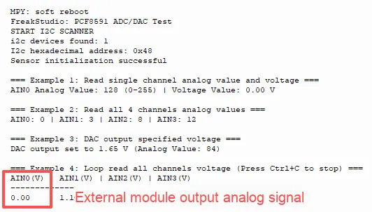
The module continuously detects and outputs the voltage of each pin. Only AIN0 is connected to the output signal of the slide rheostat module, while all other channels are in a floating state, leading to random voltage fluctuations. These unstable channels can be directly ignored.
Turn the sliding rheostat module to adjust the voltage:
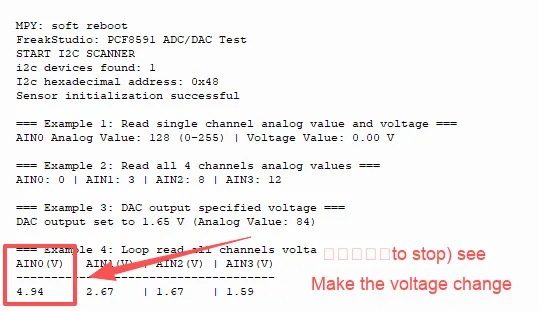
Measure with a voltmeter AOUT output:

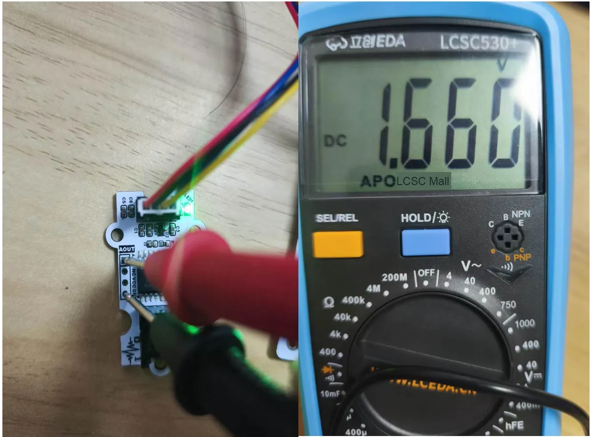
Measured 1.66V, which is basically correct.
IV. Drivers
pcf8591_driver-1.0.2.zip 16 KB
5. BOM & Recommended Alternative Parts
None.
6. Revision History
Document Version | Date of Revision | Modifier | Modified Content |
v1.0 | 2026-03-27 | Ling Gaoxing | Initialize the document |
v1.0.1 | 2026-04-21 | Li Zisheng | The production documents have not been exported yet, while all the others have been sorted out completely. |
v1.1 | 2026-04-23 | Xin Ruili | Create an open version of the document, based on the internal document version v1.0.1. |
VII. Relevant Materials
7.1 Chip Datasheet
PCF8591.pdf 232 KB
7.2 Unique Icons for PCB Silk Screen