Contents
- I. Module Introduction
- II. Introduction to Main Chips
- 2.1 Chip Overview
- 2.2 Pin Definition
- 2.3 Functional Block Diagram
- 2.4 Performance Parameters
- 2.5 Reference Circuit
- 2.6 Chip Configuration
- 2.7 Communication Interfaces and Related Protocols
- 2.8 PCB Routing Notes
- III. Circuit Engineering
- 3.1 Circuit Source Engineering
- 3.2 Module Usage Instructions
- 3.3 Application Experiment
- IV. Drivers
- 5. BOM & Recommended Alternative Parts
- 6. Revision History
- VII. Relevant Materials
- 7.1 Chip Datasheet
- 7.2 Unique Icons for PCB Silk Screen
I. Module Introduction
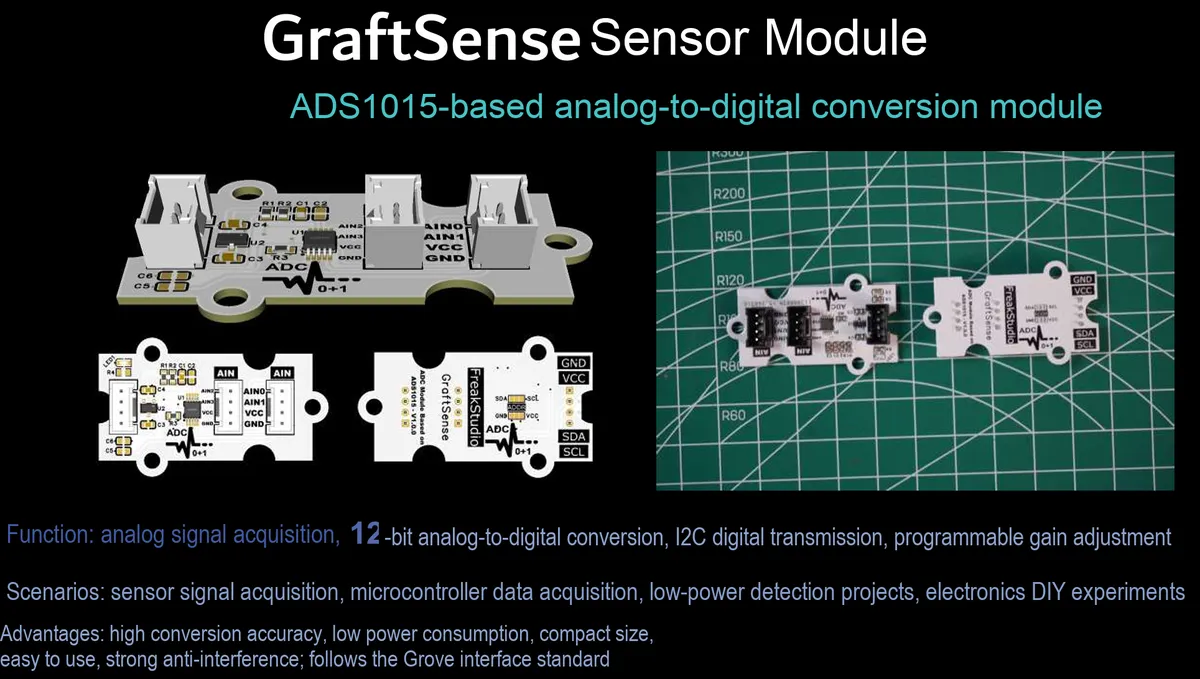
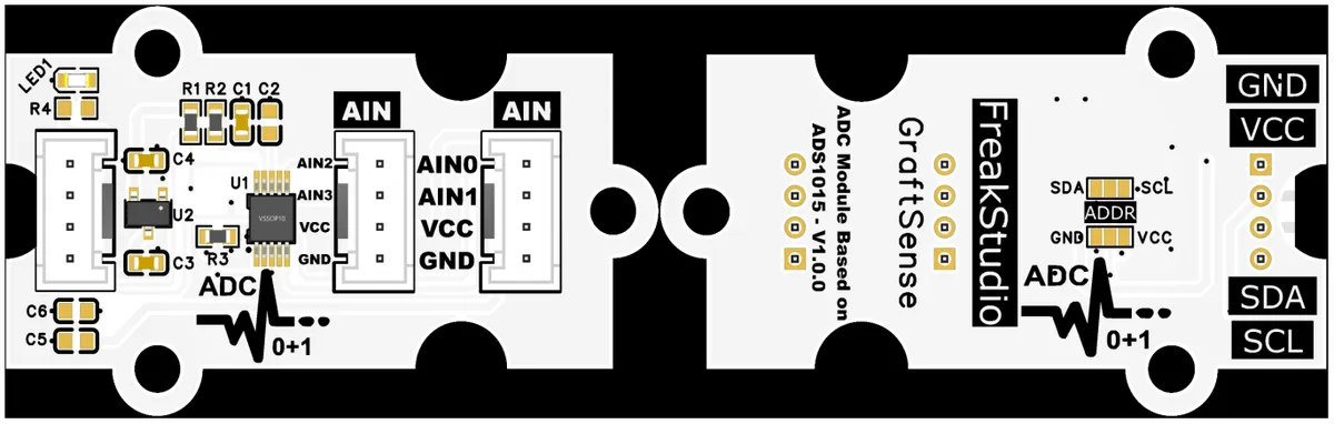
ADS1015-Based Analog-to-Digital Conversion Module, which adopts the TI ADS1015 12-bit high-precision ADC chip solution, has a built-in 6-range programmable gain amplifier, supports a wide range of analog input from ±0.256V to ±6.144V, and features a maximum sampling rate of 3300 SPS;Compatible with I²C communication interface, the slave address can be switched via the ADDR pin to support multi-chip cascading. It is equipped with a 5V to 3.3V LDO voltage regulator circuit and power filter circuit, compatible with 3.3V logic level, and has an operating current of only 150μA. It is suitable for low-power portable Data Acquisition, industrial sensor monitoring, maker DIY and other scenarios, providing accurate and efficient analog signal digitization capability for the system.
II. Introduction to Main Chips
ADS1015 is a TI -launched 12-bit high-precision I²C interface ADC with built-in 128-byte SRAM and 6-stage programmable gain amplifier. It supports a maximum sampling rate of 3300 SPS, with an analog input range covering ±0.256V to ±6.144V, operates on a supply voltage of 2.0V to 5.5V, and draws a mere 150μA operating current. It can communicate with MCUs via I²C / SPI interfaces, making it suitable for low-power, high-precision analog signal acquisition scenarios.
2.1 Chip Overview
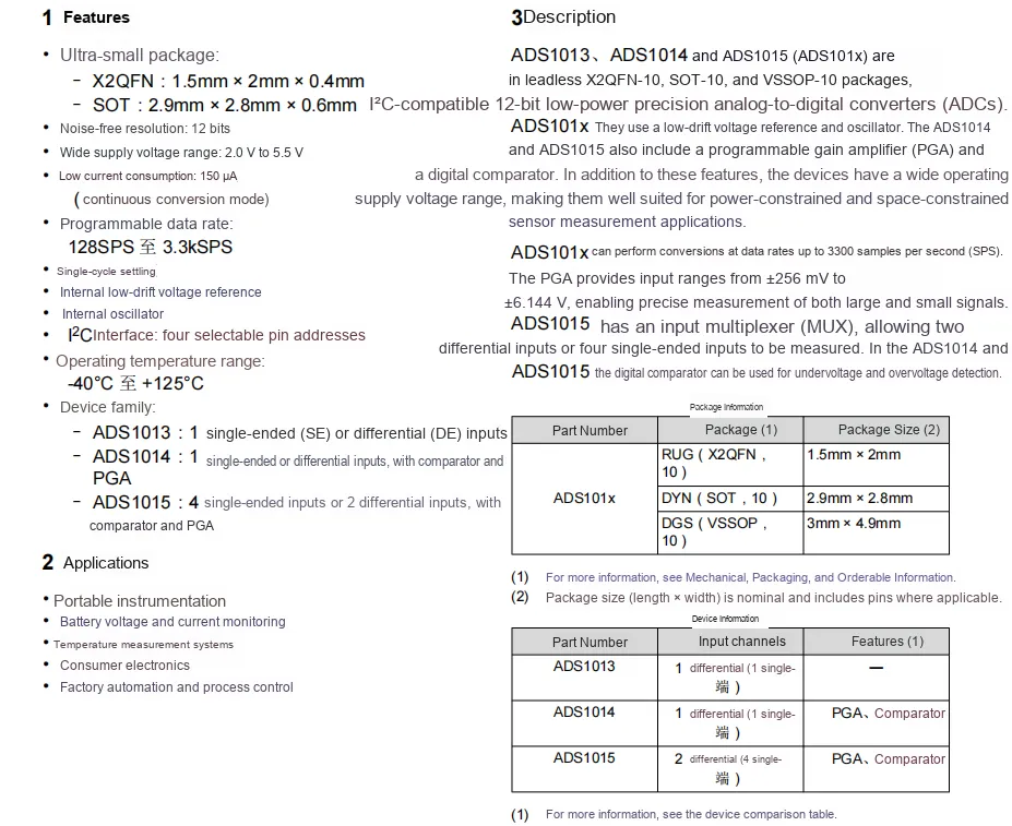
ADS1015 is TI 's newly launched 12-bit low-power precision I²C interface ADC, which integrates a programmable gain amplifier (PGA) and a digital comparator, supports 4 single-ended / 2 differential analog inputs, features a sampling rate ranging from 128 SPS to 3.3 kSPS, operates on a supply voltage of 2.0 V to 5.5 V with a working current of only 150 μA, and allows configurable I²C slave addresses, making it ideal for low-power, high-precision analog signal acquisition scenarios.
2.2 Pin Definition
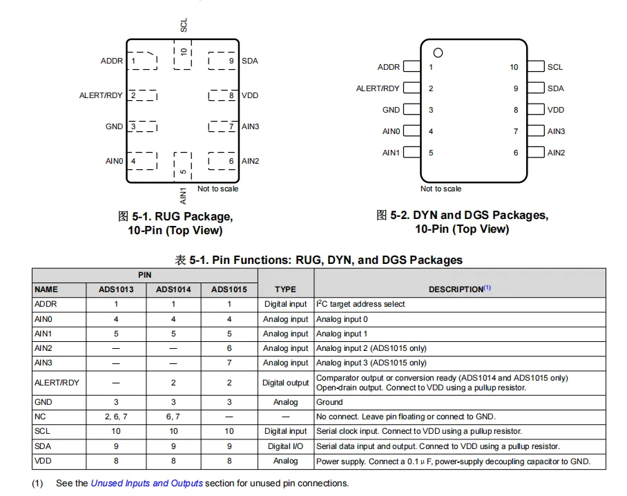
ADS1015 Pin Definitions and Package Outline: It is available in three 10-pin packages: RUG / DYN / DGS. The core pins include the I²C interface (SCL / SDA, requiring external pull-up resistors), the address selection pin ADDR, 4 analog inputs (AIN0 ~ AIN3), the digital comparator output ALERT / RDY, as well as power and ground pins, enabling reliable I²C communication and high-precision analog signal acquisition.
2.3 Functional Block Diagram
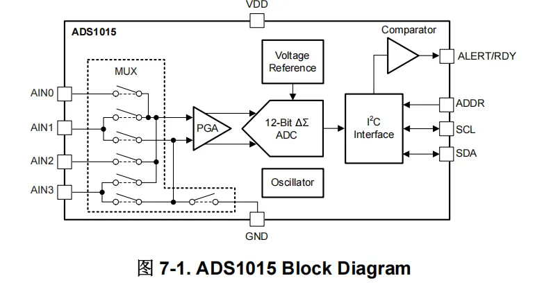
ADS1015 ’s core operating principle is as follows: 4 analog inputs (AIN0 to AIN3) are selected by a programmable multiplexer (MUX), then sent to a programmable gain amplifier (PGA) to amplify small signals, covering an input range of ±0.256V to ±6.144V. The amplified signal is fed into a 12-bit ΔΣADC core, which, driven by the internal reference voltage and oscillator, completes analog-to-digital conversion at a rate of 128SPS to 3.3kSPS.The conversion result is communicated with the I²C interface (SCL / SDA) and the MCU. Meanwhile, the built-in digital comparator can output an out-of-limit or conversion completion signal through the ALERT / RDY pin, realizing low-power, high-precision analog signal digitization.
2.4 Performance Parameters
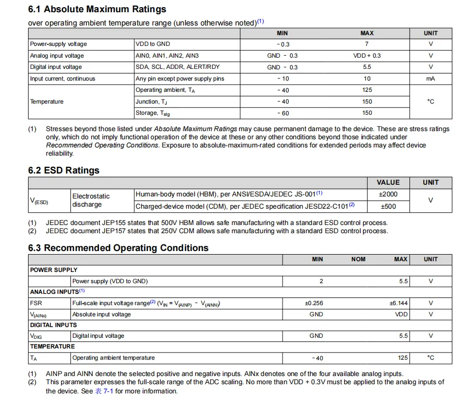
ADS1015 Absolute Maximum Ratings and Recommended Operating Conditions: Under absolute maximum ratings, the logic supply VDD ranges from -0.3V to 7V, the analog input voltage ranges from GND −0.3V to VDD + 0.3V, and the operating temperature ranges from -40°C to 125°C; the recommended operating conditions are VDD = 2V ~ 5.5V, the analog input full-scale range is ±0.256V ~ ±6.144V, it is compatible with 3.3V level, and is suitable for stable, reliable, low-power and high-precision analog acquisition scenarios.
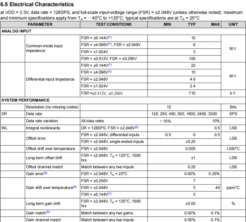

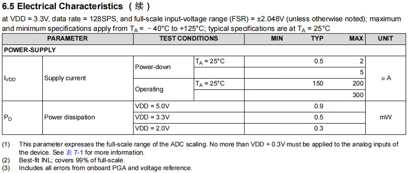
ADS1015 Electrical Characteristics: At VDD = 3.3V and a sampling rate of 128 SPS, it is a 12-bit high-precision ADC with no missing codes, featuring an integral non-linearity ≤ 0.5 LSB, analog input impedance that varies with the measurement range; it operates at a mere 150 μA with power consumption as low as 0.5 mW, is compatible with 3.3V logic levels, and has clear high and low level thresholds for its digital interface, making it ideal for low-power, high-precision analog signal acquisition applications.
2.5 Reference Circuit
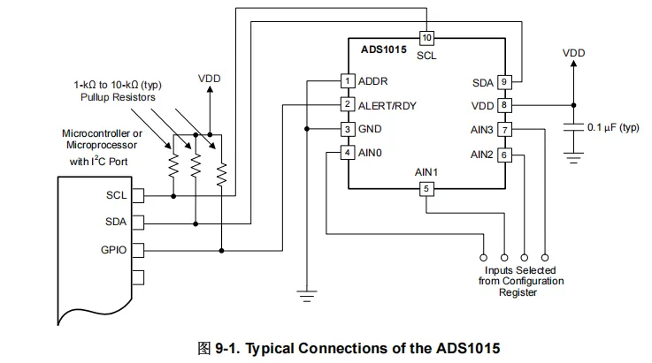
ADS1015 typical application circuit: It communicates with I²C interface via MCU, SCL / SDA pins are each connected with a 1kΩ~10kΩ pull-up resistor; the ADDR pin can configure the slave address, and the ALERT / RDY pin is connected to MCU GPIO for interrupt notification;VDD is connected to a 2.0V~5.5V power supply with a 0.1μF filter capacitor, and the 4 analog inputs (AIN0 ~ AIN3) can be configured as single-ended or differential input to achieve low-power and high-precision analog signal acquisition.
2.6 Chip Configuration
None.
2.7 Communication Interfaces and Related Protocols
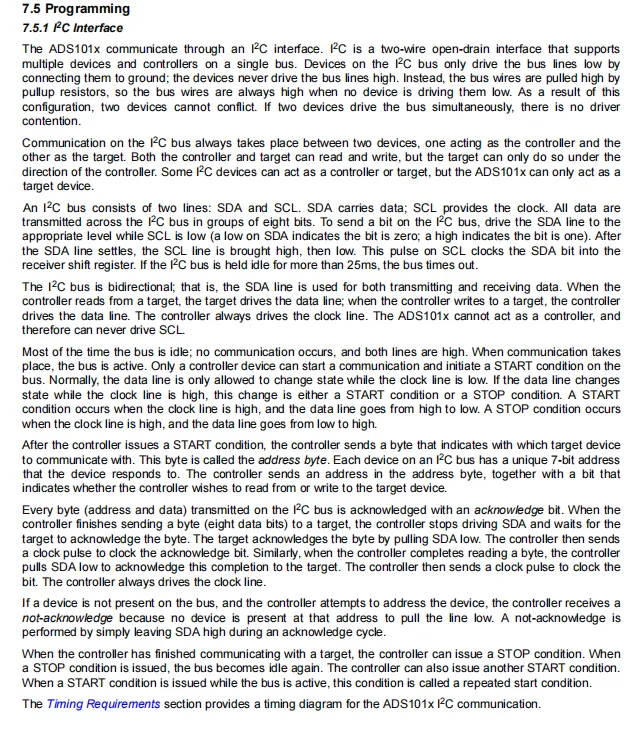
Adopts I²C two-wire open-drain interface, only acts as a slave to communicate with MCU, and external pull-up resistors are required for SCL / SDA; it complies with standard I²C timing, initiates/terminates transmission with START / STOP conditions, selects the slave address via address bytes, followed by an ACK acknowledgment after each byte, supports repeated START operations, and enables stable multi-device communication and high-precision ADC data read and write.
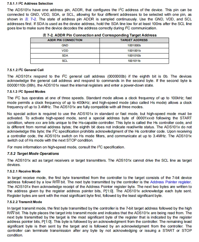
Four I²C slave addresses (0x48 / 0x49 / 0x4A / 0x4B) can be configured via the ADDR pin; it supports three speed modes of 100kHz/400kHz/3.4MHz and responds to general call addresses. As a slave, it can only receive/transmit data, follows the address pointer register operation, transmits high bytes first, and realizes stable and reliable multi-device high-precision ADC data interaction.
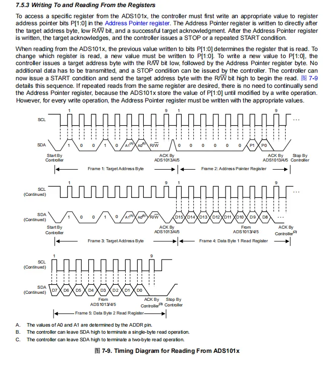
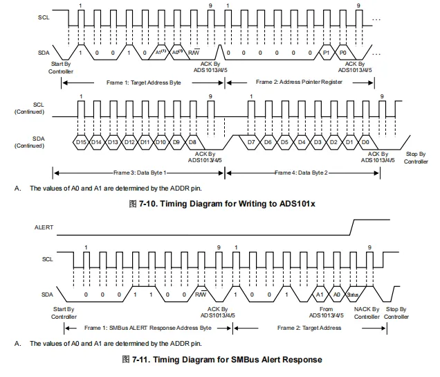
The MCU first writes to the address pointer register via I²C to specify the target register address; when reading, it first sends the address and read command, then the ADS1015 outputs the 16-bit conversion result in high-byte-first order, with an ACK response following each byte. It supports repeated read operations to achieve precise and efficient ADC register access and data reading.
2.8 PCB Routing Notes
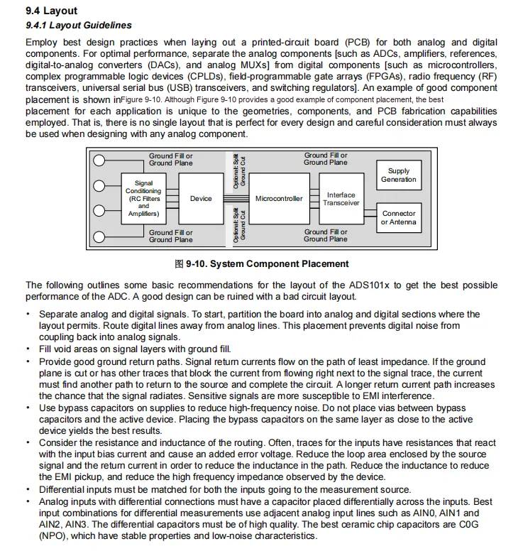
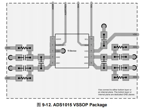
ADS1015 's PCB Layout Guide: The core is analog and digital partition layout , separating analog/digital signals, using complete planar and nearby decoupling capacitors, optimizing signal return path and wiring impedance, differential inputs need to match wiring and use low noise capacitors to reduce noise interference and achieve high precision and low noise performance of ADC .
III. Circuit Engineering
3.1 Circuit Source Engineering
To obtain the circuit source project, please follow the official account [Freak Embedded].
3.2 Module Usage Instructions
The schematic diagram of this module is shown below:
ads1015.pdf 2.5 MB
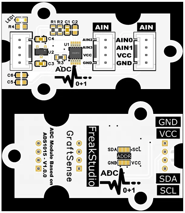
This module provides an IIC communication interface: it supports a maximum standard I²C communication rate of 400kHz, and can switch between 4 types of I²C pin to realize multi-chip cascading. Each of the ADDR pin to realize multi-chip cascading. Each of the SCL / SDA pins is connected to a 4.7kΩ pull-up resistor to comply with the I²C specification, is compatible with 3.3V level, and can stably transmit ADC configuration commands and 12-bit conversion data. Combined with the built-in programmable gain amplifier to achieve high-precision analog signal acquisition, it is suitable for scenarios such as low-power sensor monitoring, portable instruments and maker DIY, providing the system with reliable and efficient analog signal digital interaction capabilities.
The Data Acquisition AIN interface adopts the Grove interface specification and can be connected to other electronic modules with analog output.
3.3 Application Experiment
Here, we use the GraftPort-RP2040 development board for testing, and the ADS1015-based analog-to-digital conversion module uses the I2C interface to communicate with the main controller.
Here, we first use the HY2.0-4P cable to connect the module to the GraftPort-RP2040 development board's I2C0 interface, then connect the GL5516-based light intensity sensor module via the HY2.0-4P cable to the ADS1015-based analog-to-digital conversion module 's AIN0 interface:
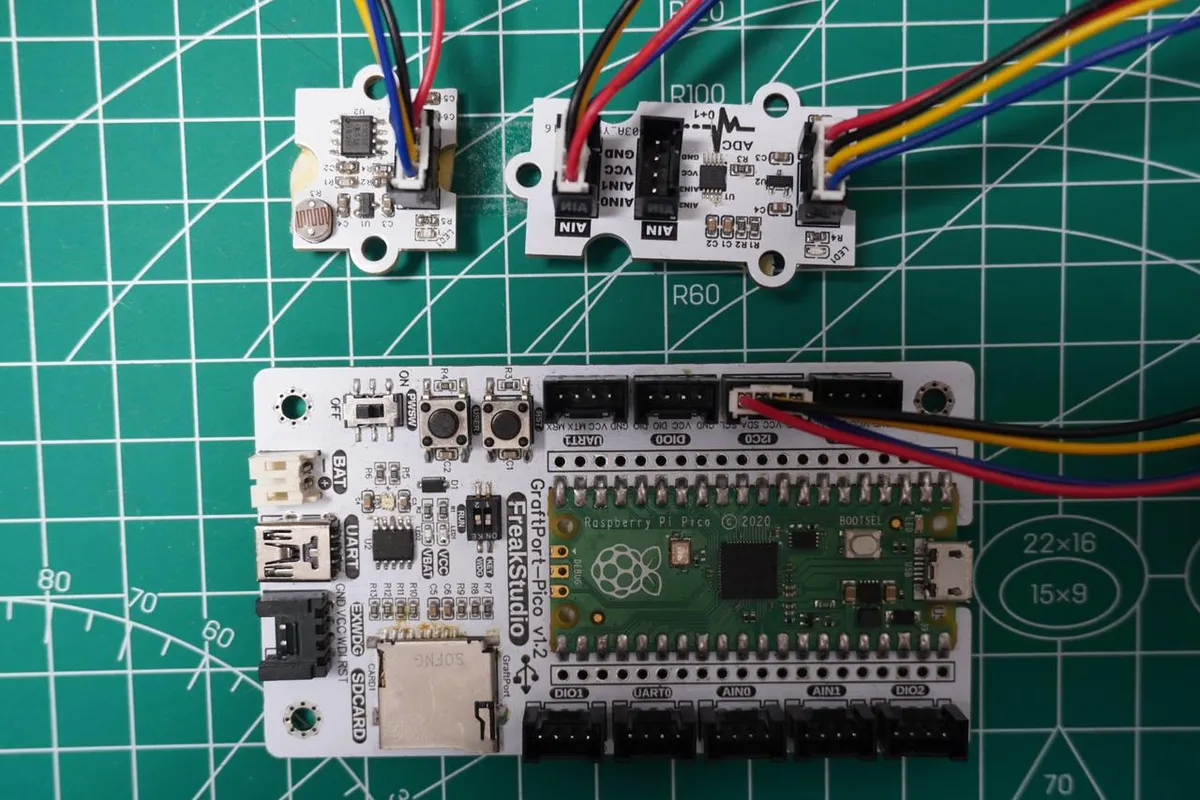
The module connections are shown in the following table:
Development Board Pins | Module Pins | Description |
Pin 4 |
|
|
Pin 5 |
|
|
- |
|
|
Here, we need to search for the relevant driver packages on uPyPI: https://upypi.net/zh/
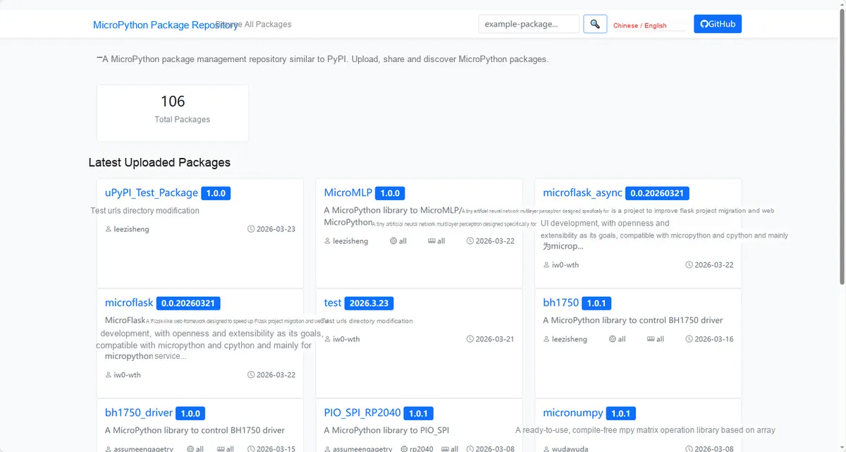
Enter ads1015_driver to search, and the following will be displayed:
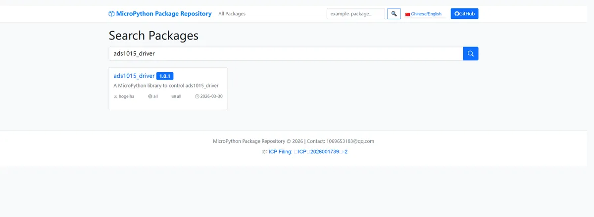
Click to copy the local installation command:
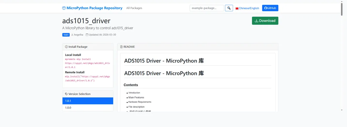
Import the module driver library code via the mip tool. Below are the usage commands for the mpremote tool:
mpremote mip install https://upypi.net/pkgs/ads1015_driver/1.0.0Import the ADS1015-based analog-to-digital conversion module - MicroPython driver code, then copy the following main.py code into our project:
# Python env   : MicroPython v1.23.0
# -*- coding: utf-8 -*-
# @Time    : 2026/3/13 PM 4:52
# @Author  : mcauser
# @File    : main.py
# @Description : ADS1015 reads voltage and controls GPIO pin level toggling. Acquires channel 0 voltage via ADS1015, periodically toggles the GPIO16 output level and reads it back for verification

# ======================================== Import Modules =========================================

import time
from machine import I2C, Pin
from ads1015 import ADS1015

# ======================================== Global Variables ============================================

# ADS1015 gain settings and corresponding ranges (V): 0=6.144 | 1=4.096 (suits 3.3V) | 2=2.048 | 3=1.024 | 4=0.512 | 5=0.256
gain_to_voltage = [6.144, 4.096, 2.048, 1.024, 0.512, 0.256]
# ADS1015 12-bit ADC maximum raw value
ads1015_max = 2047
# Initial state of the output pin
output_state = 0

I2C_SCL_PIN = 5
I2C_SDA_PIN = 4
I2C_FREQ = 400000
TARGET_ADS1015_ADDR = 0x48

# ======================================== Initialization configuration ===========================================

time.sleep(3)
print("FreakStudio: ADS1015 voltage read and GPIO pin level control")

# Initialize the I2C bus
i2c_bus = I2C(0, scl=Pin(I2C_SCL_PIN), sda=Pin(I2C_SDA_PIN), freq=I2C_FREQ)

# Scan I2C devices
devices_list: list[int] = i2c_bus.scan()
print("START I2C SCANNER")

if len(devices_list) == 0:
    print("No i2c device !")
    raise SystemExit("I2C scan found no devices, program exited")
else:
    print("i2c devices found:", len(devices_list))

# Initialize ADS1015
ads = None
for device in devices_list:
    if device == TARGET_ADS1015_ADDR:
        print("I2c hexadecimal address:", hex(device))
        try:
            ads = ADS1015(i2c=i2c_bus, address=device)
            ads.gain = 1
            print("ADS1015 sensor initialization successful")
            break
        except Exception as e:
            print(f"ADS1015 Initialization failed: {e}")
            continue
else:
    raise Exception(f"No ADS1015 sensor found (target address: {hex(TARGET_ADS1015_ADDR)})")

# ========================================  Main Program  ============================================

try:
    print("Start reading AIN0 data (Pin16 outputs high/low level)...")
    count = 0
    while True:

        raw_value = ads.read(0)
        # Calculate the actual voltage
        voltage = raw_value * gain_to_voltage[ads.gain] / ads1015_max

        # Print the data
        print(f"AIN0 raw value: {raw_value:4d} | Actual voltage: {voltage:.4f}V |")

        time.sleep(0.5)

except Exception as e:
    print(f"Error: {e}")
Burn the code, open the terminal, and the output is as follows:
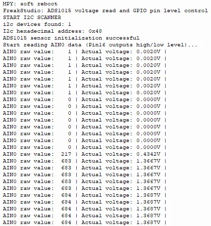
Here, it can be seen that we have successfully read the voltage value on channel 0 (i. e., the light intensity sensor module based on GL5516 corresponding voltage output).
IV. Drivers
ads1015_driver-1.0.1.zip 14 KB
5. BOM & Recommended Alternative Parts
None.
6. Revision History
Document Version | Date of Revision | Modifier | Modified Content |
v1.0 | 2026-03-27 | Ling Gaoxing | Initialize the document |
v1.0.1 | 2026-04-05 | Li Zisheng | The homepage photo has not been taken, the production files have not been exported yet, and all other items have been sorted out completely. |
v1.0.2 | 2026-04-05 | Li Zisheng | Modified main.py. |
v1.0.3 | 2026-04-21 | Li Zisheng | The production documents have not been exported yet, while all the others have been sorted out completely. |
v1.1 | 2026-04-23 | Xin Ruili | Create an open version of the document based on the internal document version v1.0.3. |
VII. Relevant Materials
7.1 Chip Datasheet
ads1015.pdf 2.5 MB
7.2 Unique Icons for PCB Silk Screen