Contents
- I. Module Introduction
- II. Introduction to Major Chips
- 2.1 Chip Overview
- 2.2 Pin Definition
- 2.3 Functional Block Diagram
- 2.4 Performance Parameters
- 2.5 Reference Circuit
- 2.6 Chip Configuration
- 2.7 Communication Interfaces and Related Protocols
- 2.8 PCB Routing Precautions
- III. Circuit Engineering
- 3.1 Circuit Source Engineering
- 3.2 Module Usage Instructions
- 3.3 Application Experiment
- IV. Drivers
- 5. BOM & Recommended Alternative Parts
- VI. Revision History
- VII. Relevant Materials
- 7.1 Chip Datasheet
- 7.2 Unique Icons for PCB Silkscreen
I. Module Introduction
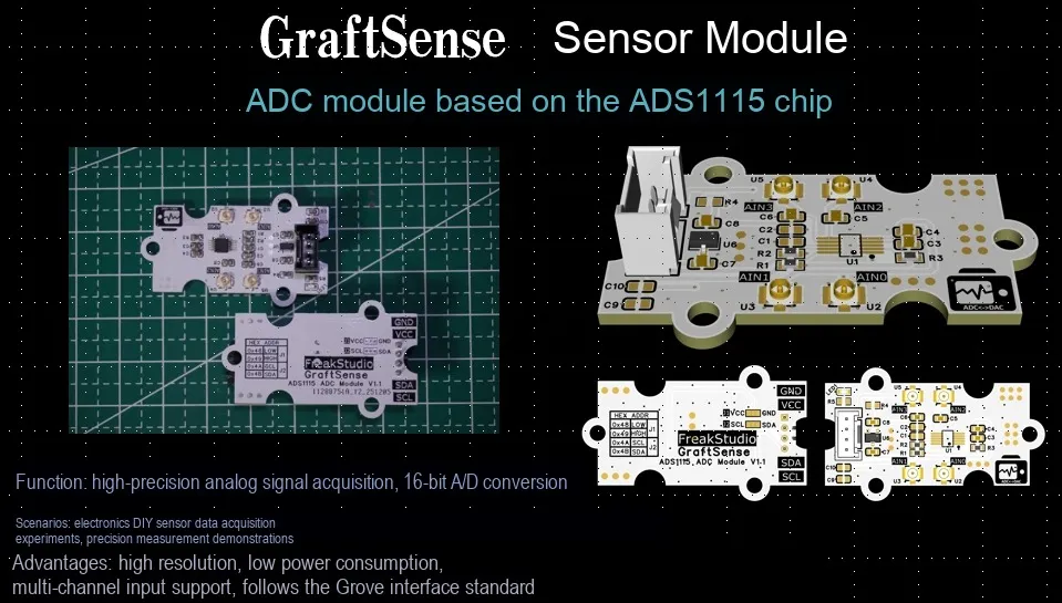
Analog-to-Digital Conversion Module Based on ADS1115 Chip, which adopts the 16-bit ADS1115IDGSR analog-to-digital converter (ADC), is equipped with 4 analog-to-digital conversion channels and a maximum sampling rate of 860 SPS. This module communicates via the I2C interface, and different communication addresses can be configured by setting the short-circuit mode. It is applicable to various scenarios requiring high-precision analog-to-digital signal conversion, providing a reliable and flexible solution for the analog-to-digital conversion demands of embedded systems.
II. Introduction to Major Chips
ADS1115 is a low-power 16-bit high-precision analog-to-digital conversion (ADC) chip with a built-in programmable gain amplifier (PGA), supporting 4-channel differential or 8-channel single-ended inputs, a maximum sampling rate of 860 SPS, high measurement accuracy and low noise.It communicates with the main controller via the I²C interface, supports a supply voltage range of 2.0V to 5.5V, features programmable data rates and multiple operating modes (continuous/single conversion), integrates a built-in voltage reference and oscillator without requiring any additional external components, and adopts the compact VSSOP-10 package. It is widely applied in scenarios demanding high-precision analog signal conversion, such as sensor signal acquisition, industrial inspection and medical devices.
2.1 Chip Overview
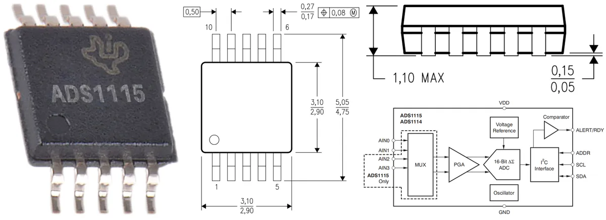
The ADS1115 is a high-precision, low-power 16-bit analog-to-digital converter (ADC) launched by Texas Instruments (TI). Integrated with multiple functions, it is suitable for a variety of analog signal acquisition and processing applications, such as sensor interfaces, voltage monitoring, and portable devices. The ADS1115 is usually connected to a microcontroller via an I²C interface; its circuit includes power supply pins (VDD, GND), SCL and SDA for I²C communication, an ADDR pin for setting the device address, and A0 to A3 as analog input pins.
The main features are as follows:
- Resolution: 16-bit, delivering high-precision data conversion
- Programmable sampling rate: up to 860 samples per second (SPS), adjustable according to application requirements
- Input Configuration: The ADS1115 is equipped with an input multiplexer (MUX) that supports four single-ended inputs or two differential inputs.
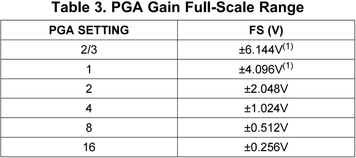
- Programmable Gain Amplifier (PGA): Built-in PGA with adjustable gain range (±6.144 V to ±0.256 V) to expand the measurable range of signals
- Interface: Standard I²C interface, supporting multi-device connection via address selection through the ADDR pin
- Low Power Consumption: In continuous mode, the current consumption is approximately 150μA, while the single-conversion mode further reduces the current consumption during standby
- Wide power supply range: It supports a wide operating power supply range from 2.0V to 5.5V
- Internal low-drift reference voltage: provides a stable reference voltage to ensure high-precision analog-to-digital conversion
- Internal Oscillator: Equipped with an internal oscillator, eliminating the need for an external clock source
2.2 Pin Definition
The ADS1115 chip provides the following pins:
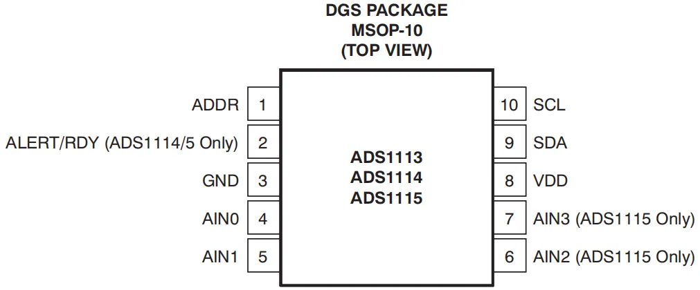
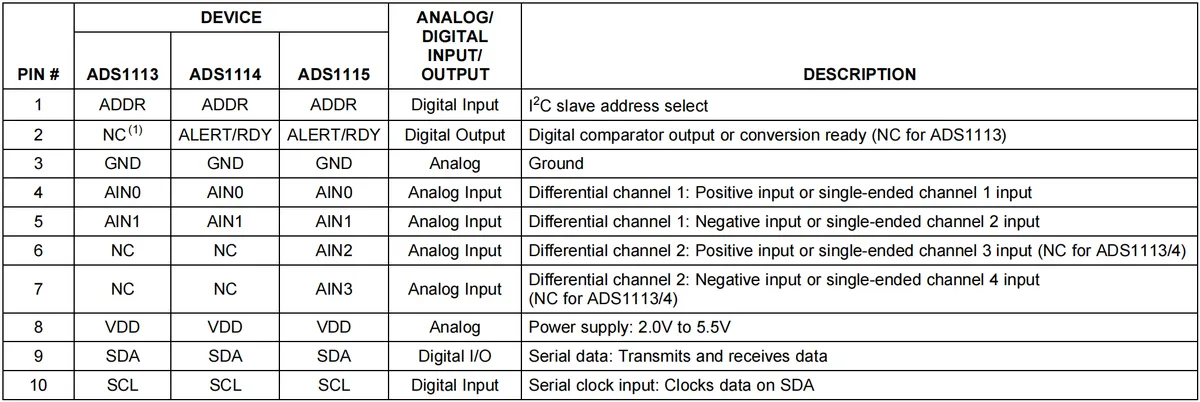
The functions of each pin are as follows:
- VDD (Power Pin): The supply voltage ranges from 2.0 V to 5.5 V, and the maximum operating current is 150 µA
- GND (Ground Pin): Connected to ground to provide a reference ground
- SCL (Serial Clock Pin): The clock line of the I²C interface, with input high voltage ranging from 0.7 × VDD to VDD + 0.3V, input low voltage ranging from 0V to 0.3 × VDD, supporting a communication rate of up to 400 kHz, and requiring an external pull-up resistor (typical value: 4.7kΩ)
- SDA (Serial Data Pin): serves as the data line of the I²C interface; it features the same electrical parameters as SCL and also requires a pull-up resistor.
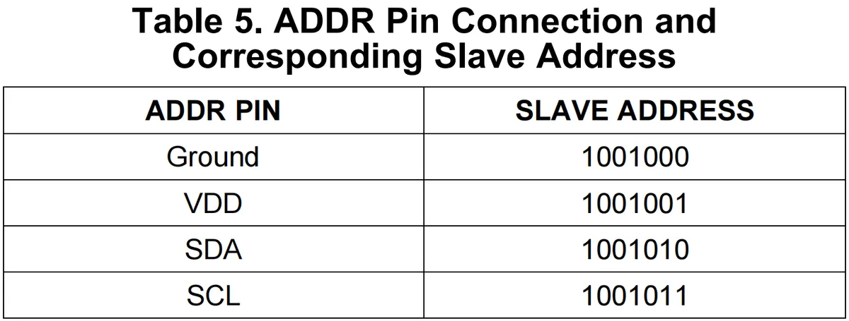
- ADDR (Address Select Pin): This pin is used to set the I²C address of the ADS1115; depending on the wiring configuration of this pin, 4 different I²C addresses are available.
- ALERT/RDY (Interrupt/Ready Pin): Can be configured as a comparator interrupt pin or a signal indicator pin when data conversion is complete; it is an open-drain output and requires an external pull-up resistor.
- AIN0, AIN1, AIN2, AIN3 (Analog Input Channels): These are four analog input channels supporting single-ended or differential input. The input voltage shall not exceed VDD + 0.3V or fall below GND - 0.3V, and the valid input voltage range is also related to the configuration of the PGA (Programmable Gain Amplifier).
2.3 Functional Block Diagram
The internal structure of the ADS1115 chip is as follows:
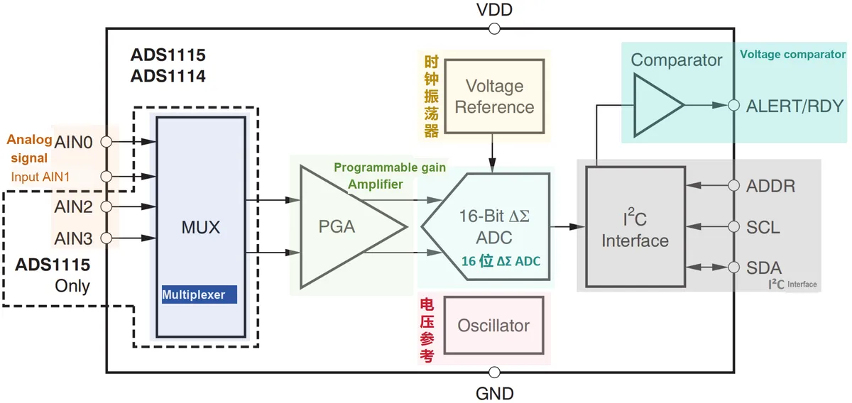
It includes the following units:
- MUX (Multiplexer): By configuring the multiplexer, we can select to use differential measurement or single-ended measurement for the four input channels (AIN0 to AIN3).
- PGA (Programmable Gain Amplifier): It amplifies the input signal and transmits it to the 16-bit ΔΣ ADC; its gain is configurable to adapt to input signals of different ranges.
- I²C interface: used for communication with an external MCU, it adopts standard SCL (clock) and SDA (data) signals, and the ADDR pin can be used to set the device address, which allows multiple ADS1115 chips to be connected to the same I²C bus
- Comparator Voltage Comparator: An optional comparator function that, in combination with the ALERT/RDY pin, can issue an interrupt signal when data is ready or a set threshold is reached.
- 16-bit ΔΣ ADC: Converts analog signals into 16-bit digital signals and transmits data via the I²C interface
- Internal Voltage Reference and Clock Oscillator: Provides a stable internal clock and voltage reference for accurate analog-to-digital conversion
2.3.1 Multiplexer
The ADS1115 has a built-in multiplexer (MUX), which allows us to select signals from multiple input channels for measurement. There are two main connection modes for input signals: differential input and single-ended input.
- Differential input: means that the signal is measured by the voltage difference between two input pins (positive input and negative input). For the ADS1115, this means it measures the voltage difference between
AINP(positive input) andAINN(negative input);Differential inputs can measure both positive and negative voltages, meaning the input range is±Vref, which is a full-scale (bipolar) range. The differential input mode can utilize the entire resolution of the ADC, where all 16 bits can be used to resolve the signal. The full-scale range is divided into 2^16 = 65536 discrete values, and the resolution is2Vref / 65536 - Single-ended input: means that the signal is input from one channel while the other channel is grounded (usually connected to
GND), and the ADC actually measures the voltage of the input signal relative to the ground; the measurement range of single-ended input is from 0 toVref, which means it can only measure positive voltages and cannot measure negative voltages, making the effective input range of the signal unipolar. The single-ended input mode only uses 15 bits of it, resulting in a 1-bit loss of resolution. The full-scale range is 2^15 = 32768 discrete values, and the resolution becomesVref / 32768
A multiplexer (MUX) is an electronic switching device used to select one from multiple signal sources as the output:
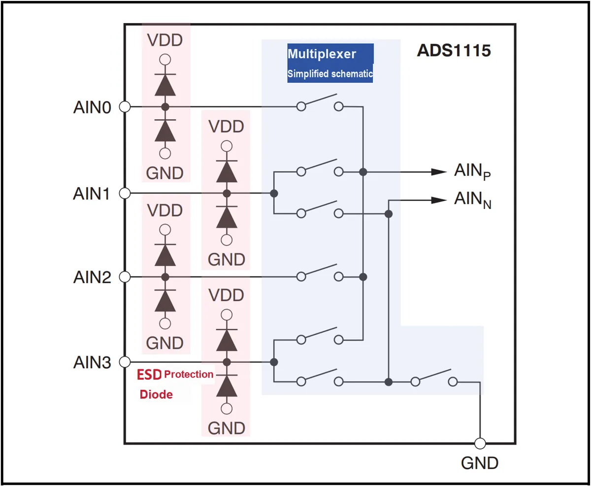
The ADS1115 allows selection of different input modes via the MUX bits in the configuration register; when measuring a single-ended signal, the MUX internally connects the negative input terminal (AINN) of the ADC to ground (GND).
The signal input channels of the ADS1115 are also equipped with electrostatic discharge (ESD) protection diodes, which are designed to safeguard the ADC inputs from overvoltage or negative voltage. To prevent these ESD diodes from turning on, the voltage of the input signal must be maintained within the following range:
GND - 0.3V < AINx < VDD + 0.3V
If the input signal is likely to exceed this range, it is recommended to use an external Schottky diode or a series resistor to limit the input current so as to protect the ADC. Meanwhile, when using the ADS1115, if some input channels are not connected to signals and may be "overdriven"(i. e., the input voltage exceeds the valid range), the conversion results of other channels may be affected. It is recommended to provide voltage clamping (e. g., via a Schottky diode) for these unused input channels to avoid impacts on the measurement.
2.3.2 Analog Signal Input
The ADS1115 employs a switched-capacitor architecture to measure differential voltages, a structure that relies on the timing of closing and opening of switches (S1 and S2) to charge and discharge the input capacitors:
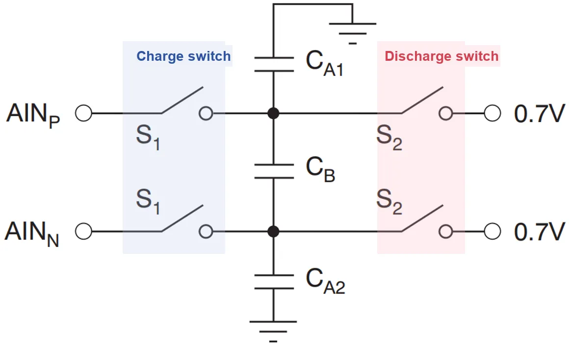
Wherein, S1 is the charging switch and S2 is the discharging switch: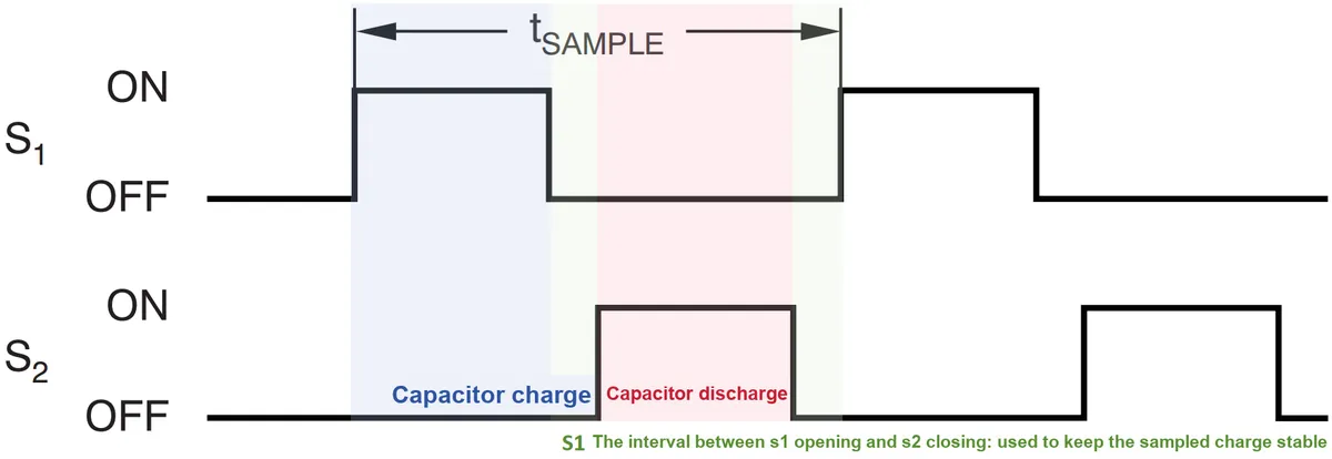
- S1 Charging Switch: S1 controls the sampling of external signals by the capacitor from the input terminals AINp and AINn. When S1 is closed, the capacitor charges and is charged to the voltage of AINp and AINn; when S1 is open, the capacitor holds the sampled voltage and prepares for discharging in the next stage.
- S2 Discharge Switch: S2 closes after S1 is turned off to initiate the discharge process; at this point, the charge in the capacitor is discharged to the reference voltage (typically 0.7V or 0V), and the purpose of this process is to prepare for the next sampling cycle.
Since the charging and discharging of the capacitor will cause transient currents, these currents are very small, but their average value can be used to calculate the effective input impedance of the ADC:
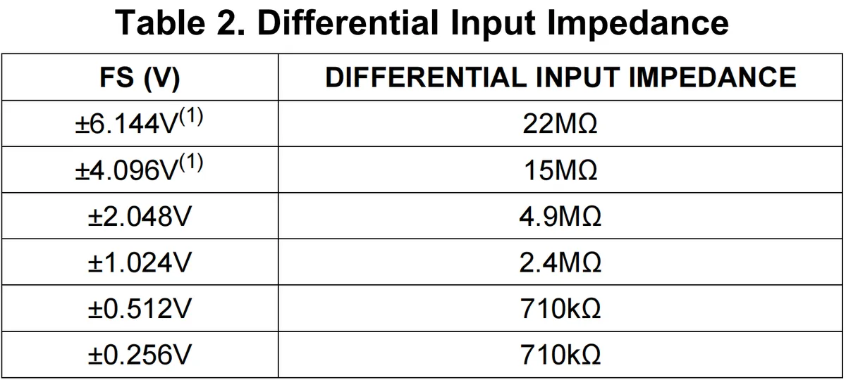
whereis the input voltage, andis the average current. When the built-in PGA of the ADS1115 uses different gains, the full-scale range of the ADS1115's ADC varies, and its input impedance also differs accordingly:
2.3.3 PGA Programmable Gain Amplifier
PGA is an amplifier whose amplification factor can be dynamically adjusted via an external control signal; it can dynamically adjust the gain according to different input voltages to ensure that the signal fits the input voltage range of the ADC.
The internal structure of PGA mainly consists of the following parts: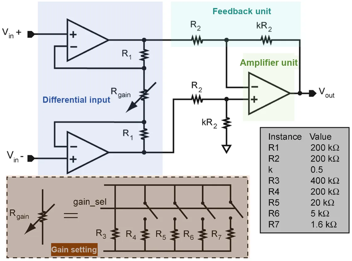
- Gain control circuit: A gain control circuit typically consists of a set of resistor networks, which select different gain settings via a switch matrix; different resistance values in the resistor networks can adjust the amplification factor of the input signal.
- Feedback Circuit: A PGA relies on feedback control to ensure the stability of the amplifier. By adjusting the feedback resistor, a PGA can control the amplification factor of the output.
- Differential Input and Output: A PGA typically adopts differential input (two input terminals: non-inverting input and inverting input) to mitigate noise interference and common-mode signals.
- Amplifier Core: This section refers to the operational amplifier, which is responsible for actual signal amplification. The op-amp receives the input signal from the gain control circuit and outputs the amplified signal according to the selected gain multiplier.
Next, we illustrate the function of PGA and its impact on the input signal range through an example. Suppose we are measuring the output of a sensor whose output analog signal fluctuates around 0.001V, while the measurement range of the ADC in use is 0~5V with a resolution of 10 bits. Then each digital step (minimum change) is 5V/1024 = 0.00488V. After ADC conversion, the calculated digital signal will always be 0, and we cannot effectively detect the tiny changes of the sensor via the ADC.
To improve the signal detection capability, we introduce a Programmable Gain Amplifier (PGA) to amplify the input signal by a factor of 100. At this point, the variation range of the input signal becomes 0.1 V. After amplification, the digital signal obtained through ADC conversion will range from 0 to 20, which allows us to observe the fluctuations of the input signal:
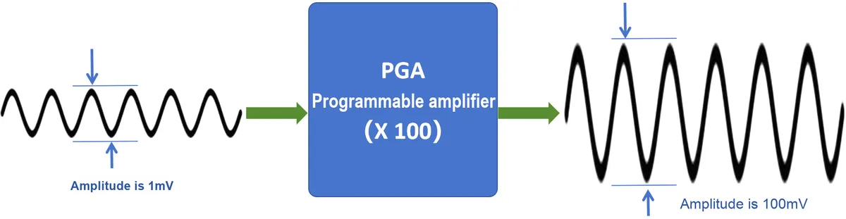
However, the use of a PGA also affects the input signal range: since the amplification factor of the PGA is 100 at this time, the signal input range is reduced by a factor of 100 accordingly, and the original input range of the ADC (0~5V) will become 0~0.05V. If we attempt to input a signal higher than 0.05V (for example, 0.1V), it will exceed the input range of the PGA, which may result in output saturation or distortion.
Selecting an appropriate PGA gain is critical to ensuring that the ADC can effectively measure signals. We need to ensure that the PGA gain setting boosts the input signal to the optimal measurement range of the ADC. Generally, the input range of an ADC is from 0 to a certain reference voltage (e. g., 0 to 3.3V), so the amplitude of the input signal should be adjusted to fall within this range. At the same time, it is essential to ensure that the PGA gain setting does not cause the output signal to exceed the maximum input voltage of the ADC (e. g., 3.3V).
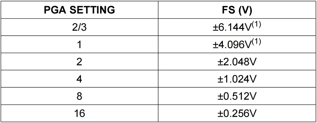
The ADS1115 integrates a Programmable Gain Amplifier (PGA) to amplify input signals, and this PGA features multiple gain settings including 2/3,1, 2,4, 8 and 16; under different gain settings of the PGA, the full-scale input range varies, meaning the maximum analog input voltage range that the ADC can accept will change accordingly:
2.3.4 ADC Analog-to-Digital Conversion Unit
The ADS1115 stores the result of analog-to-digital conversion of analog signals in two's complement format: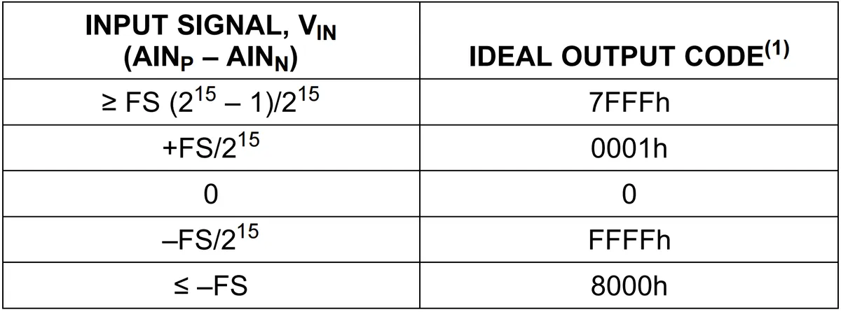
- When the input signal reaches the maximum positive value that can be stored, the value of the register corresponding to the ADC for storing the conversion result is
7FFFh, which is equivalent to 32767 in decimal. When the input signal exceeds the maximum positive value, the value of the register corresponding to the ADC for storing the conversion result remains unchanged. - When the input signal reaches the minimum negative value that can be stored, the value of the ADC register corresponding to storing the conversion result is
8000h, which is equivalent to -32768 in decimal. When the input signal exceeds this minimum negative value, the value stored in the corresponding ADC register for the conversion result remains unchanged. - The minimum resolution of the ADS1115 is related to the PGA gain setting; when the PGA gain setting changes, the full-scale range will change accordingly.
The relationship between input voltage and code conversion is shown as follows:
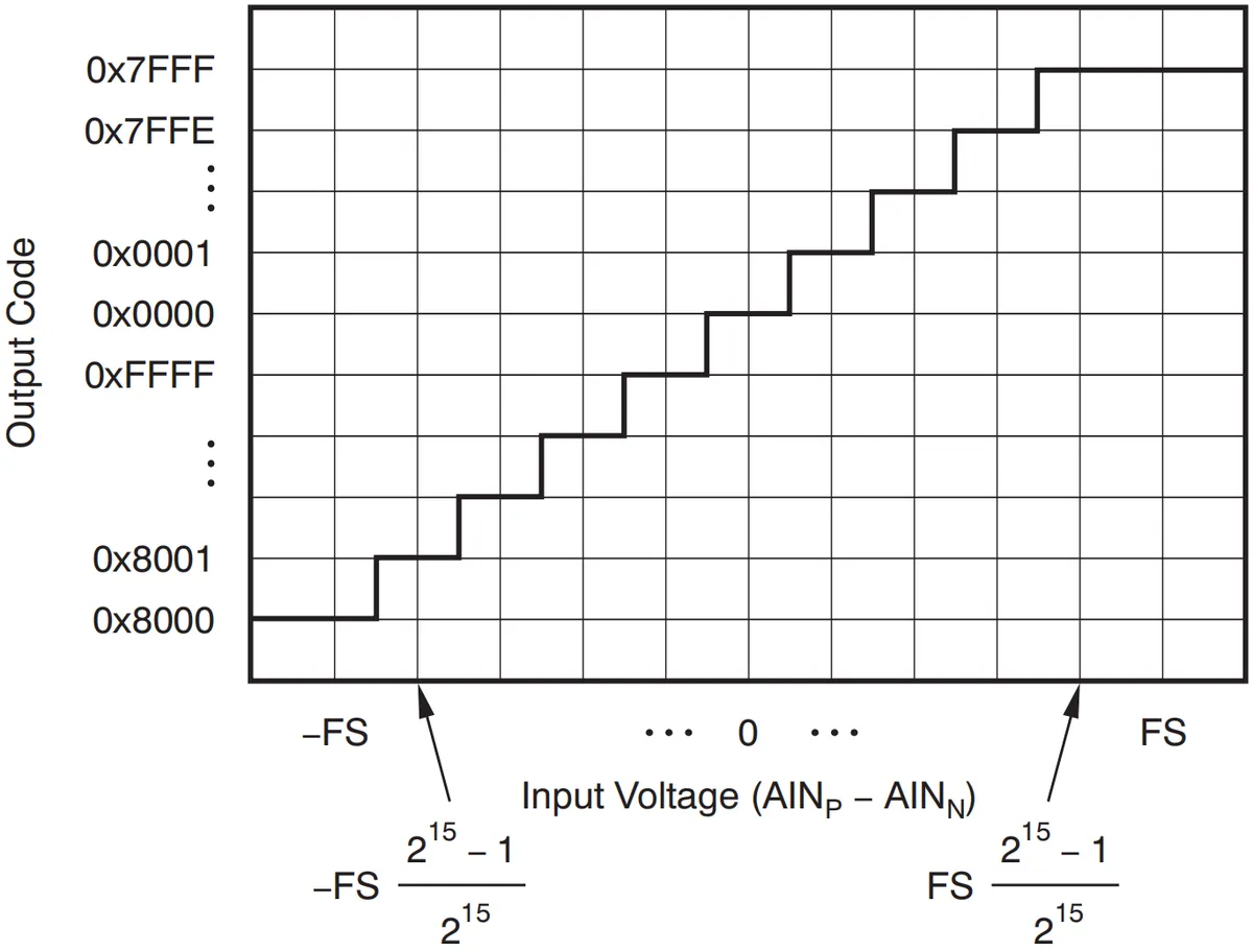
To prevent frequency-domain aliasing, the ADC data sampling rate needs to be at least twice the frequency of the input signal. The digital filter built into the ADS1115 chip can attenuate high-frequency noise to a certain extent, but in some applications, an external filter may be required. Meanwhile, when designing the input filter circuit, the interaction between the filter network and the input impedance of the ADS1115 chip needs to be taken into account.
The ADC of the ADS1115 can operate in two modes: continuous conversion mode and single-shot conversion mode.
- Continuous Conversion Mode: In this mode, the ADS1115 chip continuously performs analog-to-digital conversions; after each conversion is completed, the conversion result is stored in the conversion register, and the next conversion starts immediately.
- Single-shot conversion mode: In single-shot conversion mode, the ADS1115 waits for the OS bit in the configuration register to be set to high level. Once the OS bit is set, a single analog-to-digital conversion is initiated, and meanwhile this bit is cleared to 0 to indicate that a conversion is in progress. When the conversion data is ready, the OS bit will be set again, and the device will enter a low-power state.
2.3.5 Internal Voltage Comparator
The ADS1115 chip has a built-in voltage comparator, and the function of this comparator can be configured:
- Traditional Comparator: In this mode, the
ALERT/RDYpin is triggered (active-low by default) when the converted data exceeds the limit set in the high-threshold register; the comparator releases the trigger when the input signal falls below the value of the low-threshold register. - Window Comparator: In this mode, if the converted data exceeds the upper threshold register or falls below the lower threshold register,
ALERT/RDYpin will be triggered.
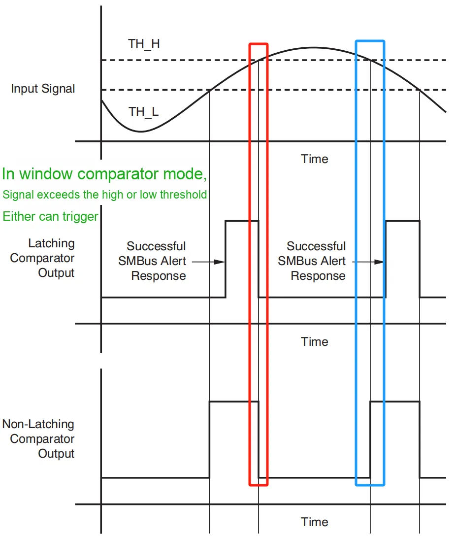
At the same time, this voltage comparator also features COMP_LAT latch bit, which can be configured to keep the comparator active after triggering even if the input signal no longer exceeds the threshold; the COMP_POL polarity setting bit of the voltage comparator can configure the ALERT/RDY pin to be active high or active low.
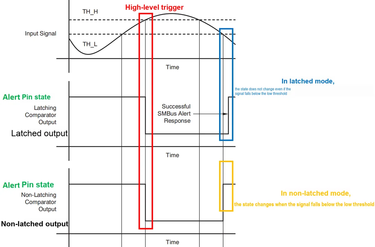
Meanwhile, the comparator can be configured to wait for a certain number of signal crossings above the threshold before triggering once the threshold is reached, the COMP_QUE bit can be set to wait for 1,2, or 4 readings exceeding the threshold, and COMP_QUE can also disable the comparator function.
And the ALERT/RDY pin, according to the configuration of the register, it can be used as an alarm pin, or as a data preparation completion signal, see 2.3.4 section, the voltage comparator threshold register section .
2.3.6 Connection of ADS1115 Chip to Microcontroller
When using the ADS1115 to acquire external signals, the common connections are as follows:
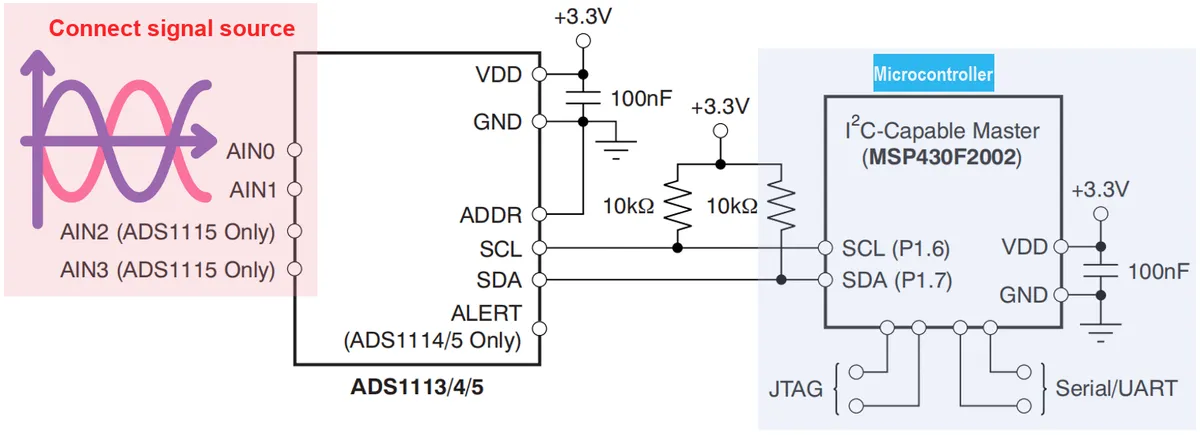
Among them, the VDD pin is externally connected with a filter capacitor to ensure stable power supply; the ADS1115 is connected to the microcontroller via the I2C interface, and at the same time ALERT pin also needs to be connected to a pull-up resistor.
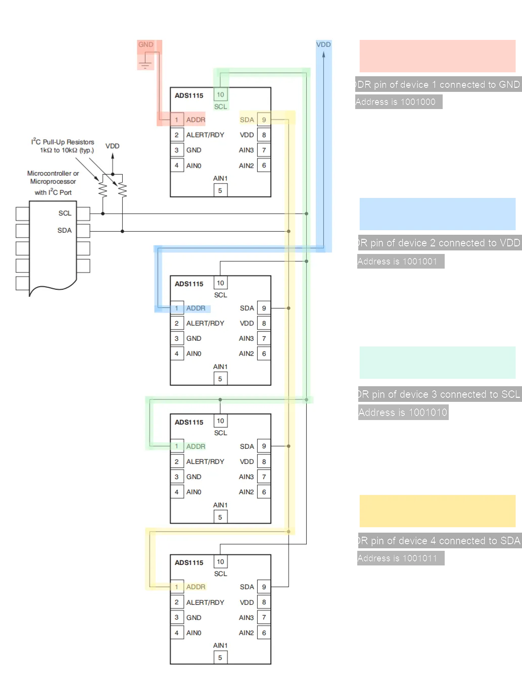
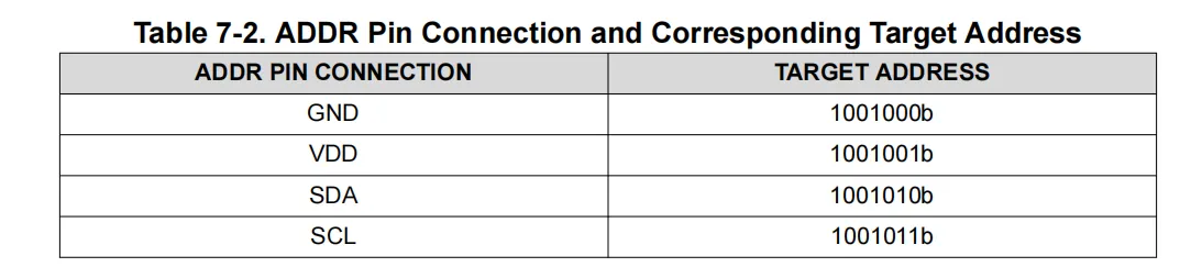
Each ADS1113/4/5 can be configured with a different I²C address via the address pin (ADDR), allowing up to four devices to be connected to the same bus:
2.4 Performance Parameters
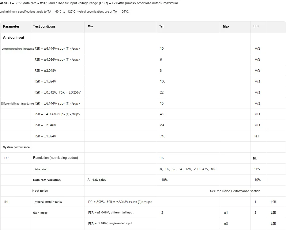
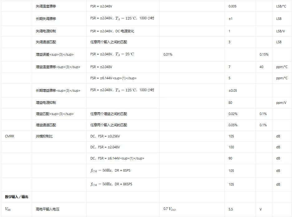

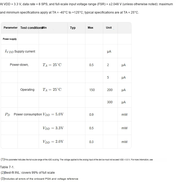
ADS1115 has the following partial performance parameters:
- Power Supply Characteristics:
- Power-down mode current typical 0.5μA, maximum 2μA (TA = 25∘C);
- Operating Mode Current Typical 150μA, Maximum 200μA (TA = 25∘C);
- Power consumption is typically 0.9 mW when VDD = 5.0 V, typically 0.5 mW when VDD = 3.3 V, and typically 0.3 mW when VDD = 2.0 V.
- Analog Input:
- The common-mode input impedance ranges from 3 MΩ to 100 MΩ depending on the full-scale range (FSR);
- Differential input impedance varies from 2.4 MΩ to 710 kΩ depending on the FSR.
- System Performance:
- 16-bit resolution;
- The data rate is available in multiple specifications including 8,16, and 32;
- Integral Non-Linearity (INL) Maximum 1 LSB;
- Gain Error Typical: 0.01%~0.15%;
- Common Mode Rejection Ratio (CMRR) up to 105dB.
- Digital Input/Output:
- High-level input voltage typically 0.7 VDD, maximum 5.5V;
- Low-level input voltage Max. 0.3 VDD;
- Low-level output voltage is max. 0.4V at IOL = 3mA;
- Input leakage current - 10~10μA.
2.5 Reference Circuit
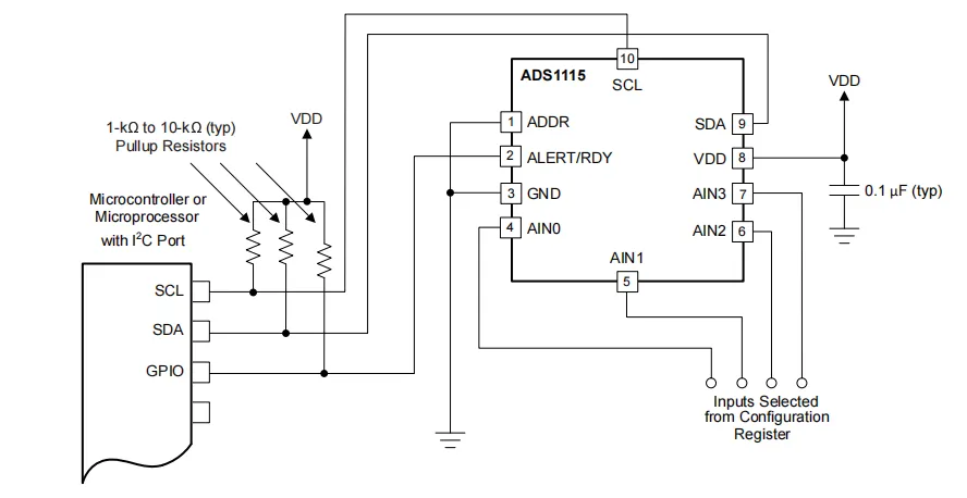
Since the I²C bus driver adopts an open-drain structure, pull-up resistors are required on both the SDA and SCL lines. The resistance values of these resistors depend on the bus operating speed and the capacitance of the bus lines. Resistors with higher values consume lower power but increase the transition time on the bus, thus limiting the bus speed; resistors with lower values allow higher speeds but result in higher power consumption. Longer bus lines have larger capacitance and require smaller pull-up resistors for compensation. Do not use excessively small resistors, otherwise the bus driver will be unable to pull the bus lines low.
2.6 Chip Configuration
The ADS111x features an ADDR address pin used to configure the device's I²C address. This pin can be connected to GND, VDD, SDA, or SCL, allowing four distinct addresses to be selected via a single pin, as shown in Table 7-2. The state of the ADDR address pin is continuously sampled. Addresses can be configured using GND, VDD, and SCL; if SDA is used as the device address, the SDA line must be held low for at least 100 ns after the SCL line goes low to ensure the device decodes the address correctly during I²C communication.
2.7 Communication Interfaces and Related Protocols
2.7.1 Introduction to Registers of the ADS1115 Chip
The ADS1115 chip features the following registers:
- Pointer Register: It is used to select the register to be accessed; by writing different values, the pointer register enables the main controller to access different registers.
- Config Register (Configuration Register): Used to configure the operating modes of the ADS1115, including input channel selection, gain setting, data rate, etc.
- Conversion Register: Used to store the result after internal ADC analog-to-digital conversion
- Lo_thresh and Hi_thresh Registers (Voltage Comparator Threshold Registers): Used to set the thresholds of the internal voltage setting comparator.
The ADS1115 performs a reset upon power-up; during the reset process, the chip sets all bits in the configuration register to their respective default values.
2.7.1.1 Pointer Register
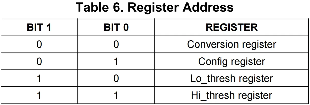
Used to select the register to be accessed, the lower two data bits are writable:

By writing different values, the pointer register enables the main controller to access different registers:
2.7.1.2 Config Register (Configuration Register)
This register is readable and writable, and has 16 data bits:
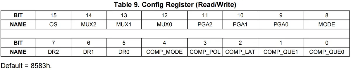
The meaning of each data bit is as follows:
data bit | Data Bit Name | Meaning |
15 | OS | Operation status / Start of single conversion: This bit controls the operation status of the device and can only be written in shutdown mode. 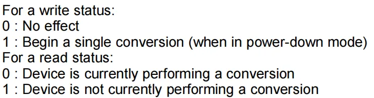 |
14-12 | MUX[2:0] | Input multiplexer configuration, used to select the input channel:  |
11-9 | PGA[2:0] | Programmable Gain Amplifier Configuration: The input voltage ranges for different configurations are as follows:  |
8 | MODE | Device operation mode control: either single conversion mode or continuous conversion mode is optional.  |
7-5 | DR[2:0] | Data Rate Control:  |
4 | COMP_MODE | Comparator mode control allows selection between a basic comparator (triggered by high/low level) or a window comparator:  |
3 | COMP_POL | Comparator polarity control allows selection of whether to output a high level or a low level after triggering: 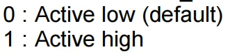 |
2 | COMP_LAT | Latch comparator control, which allows selection of whether to latch the current output level until the next state change:  |
1-0 | COMP_QUE | Number of consecutive threshold crossings that must be exceeded before triggering the 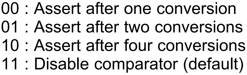 |
2.7.1.3 Conversion Register
The 16-bit conversion register holds the result of the ADC conversion, stored in two's complement format; after power-on, the conversion register is cleared to 0 and remains at 0 until the first conversion is completed.

2.7.1.4 Lo_thresh and Hi_thresh Registers (Voltage Comparator Threshold Registers)
The Lo_thresh and Hi_thresh registers of the ADS1115 are used to set the thresholds for the comparator. These registers store the upper and lower threshold values of the comparator to determine whether the input signal exceeds the set range. When the voltage of the input signal exceeds the threshold, the device can send a signal through the ALERT/RDY pin:
Lo_threshregister stores the lower threshold of the comparator, and its value indicates that when the input signal voltage is lower than this threshold, the output of theALERT/RDYpin will be deasserted or triggered, depending on the current operating mode of the comparatorHi_threshregister stores the upper threshold of the comparator, and its value indicates that when the input signal voltage is higher than this threshold, it will trigger the output of theALERT/RDYpin- Under normal circumstances,
the value of the Hi_threshregister must be greater than the value stored in theLo_threshregister.
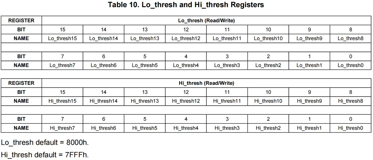
The values in these registers are stored in two's complement form: when the most significant bit (MSB, bit 15) is 0, it represents a positive number; when the most significant bit is 1, it represents a negative number.
Here, it should be noted that the ADS1115 incorporates a programmable gain amplifier (PGA), which functions to set the maximum range of the input signal and ensure that the analog signal is properly amplified or attenuated before sampling. The full-scale input voltage range (FSR) can be varied between ±6.144 V and ±0.256 V; when the PGA gain setting is modified, the resolution of the device will change accordingly, so the value of the threshold register needs to be readjusted after altering the PGA settings.
For example:
- When the PGA is set to ±6.144V, the voltage represented by 1 LSB is approximately 187.5µV
- When the PGA is set to ±0.256V, the voltage represented by 1 LSB is approximately 7.8125µV
Under different PGA gain settings, Lo_thresh and Hi_thresh registers store values corresponding to different voltage ranges.
Here, the ADS1115 also provides an ALERT/RDY pin that can function either as an alert pin or a data-ready signal depending on the register configuration.
- Alarm function: When the input signal voltage exceeds the range set by
Lo_threshorHi_thresh,the ALERT/RDYpin will send out an alarm signal, and this function is similar to a voltage comparator. - Data Ready Function (RDY Mode): In single conversion mode, after each conversion is completed,
the ALERT/RDYpin outputs theOSdata bit of the configuration register to indicate conversion completion; in continuous conversion mode,the ALERT/RDYpin generates a pulse upon the completion of each conversion. To enable this function, simply set theMSBof theHi_threshregister to 1, and set theMSBof theLo_threshregister to 0.
2.7.2 I2C Communication Interface of the ADS1115 Chip
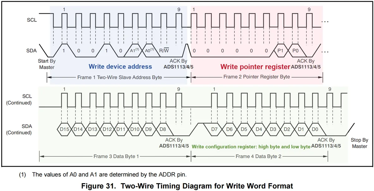
Take setting the ADS1115 chip to continuous conversion mode as an example (assuming the chip address at this time is 0x48), first it is necessary to write the corresponding configuration value to the configuration register:
- The first byte: the I²C address of the slave device to be sent
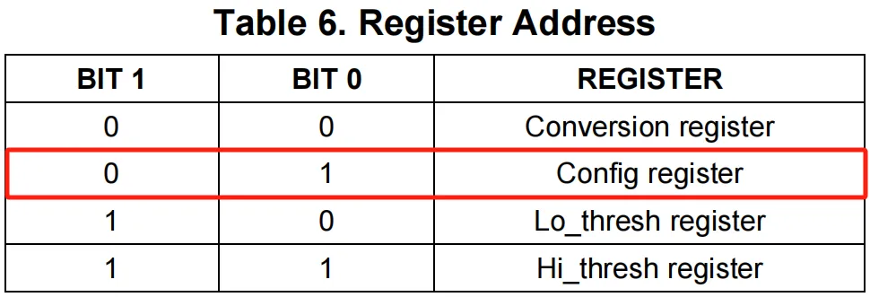
0b1001000(0x48), plus a write operation bit0 - The second byte: points to the configuration register, i. e., sends
0b00000001(0x01) to the pointer register — this byte instructs the ADS1115 chip that the subsequent data to be written is for the configuration register
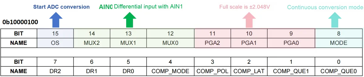
- The third byte: the MSB (most significant byte, upper 8 bits) of the configuration register, for example
0b10000100(0x84), this byte configures several primary operating modes of the ADS1113/4/5
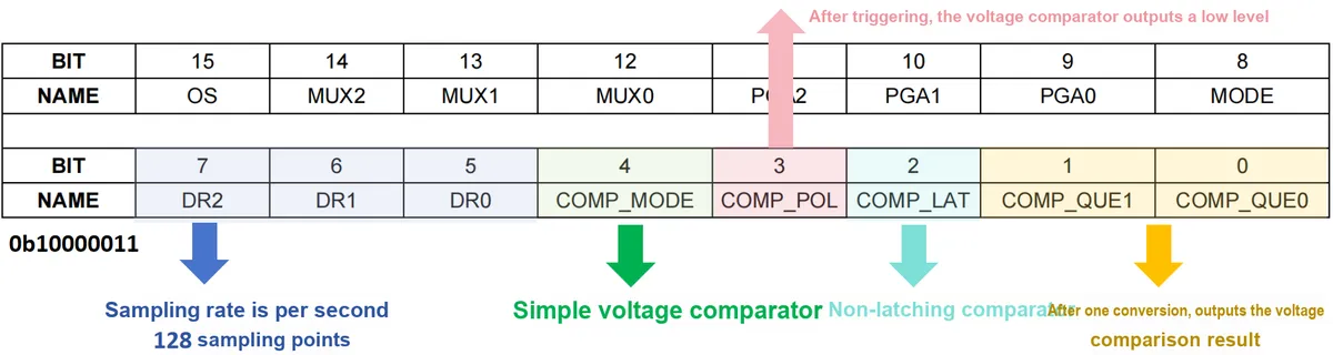
- Fourth byte: the LSB (least significant bit) part of the configuration register (lower 8 bits), for example
0b10000011(0x83), this byte contains the settings of the programmable gain amplifier (PGA), data rate and other parameters.
Here, write operations are performed on both the pointer register and the configuration register, and the I2C write format of the ADS1115 chip is as follows:
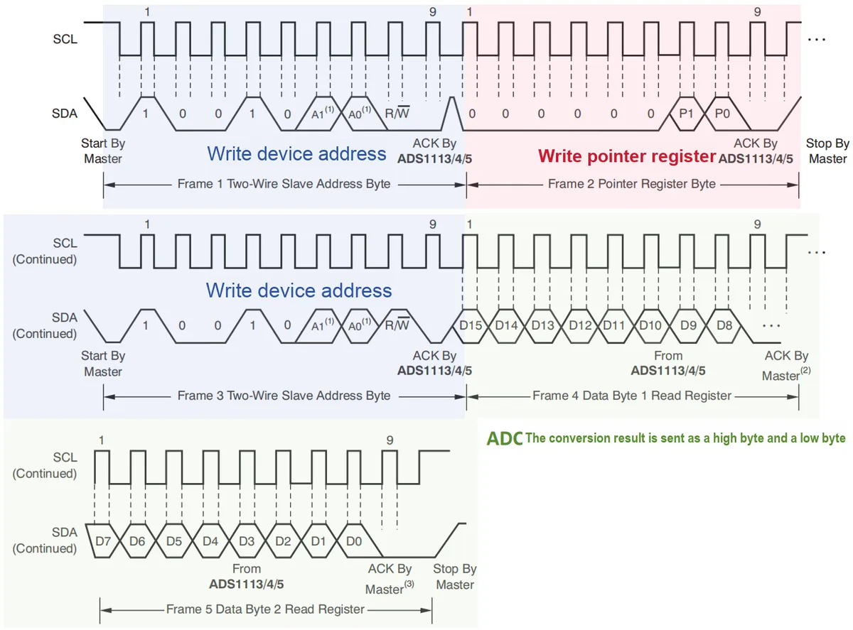
After the configuration is complete, we need to read the result after each ADC conversion. At this point, we first need to set the pointer register:
- First byte: the I²C address of the slave device to be sent
0b1001000(0x48), plus a write operation bit0 - Second byte: send to the pointer register
0b00000000(0x00) to point to the conversion register
Then read the conversion result:
- First byte: the I²C address of the slave device to be sent
0b1001000and a read operation bit1, which is0b10010001 - The second byte: The ADS1113/4/5 device will transmit the upper 8 bits (MSB) of the conversion register
- The third byte: The ADS1113/4/5 device will transmit the lower 8 bits (LSB) of the conversion register
The process of reading ADC conversion results is shown in the following figure:
2.8 PCB Routing Precautions
None.
III. Circuit Engineering
3.1 Circuit Source Engineering
To obtain the source project of the circuit, please follow the official account [Freak Embedded]
3.2 Module Usage Instructions
SCH_Schematic1_ADC Module Based on ADS1115 Chip-V1.0_2025-11-14.pdf 2.2 MB
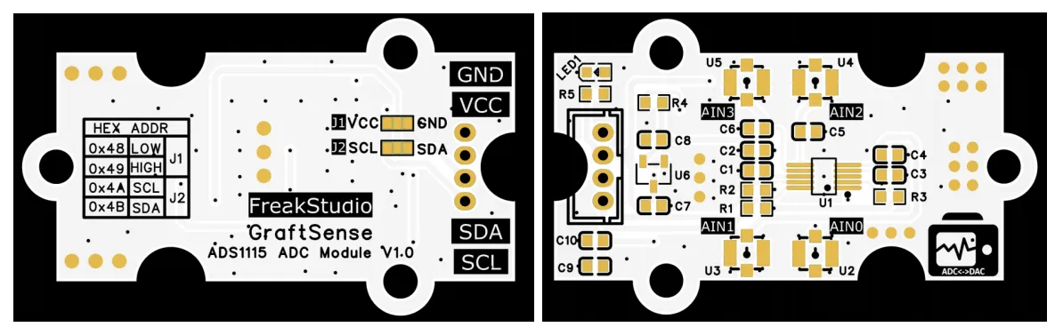
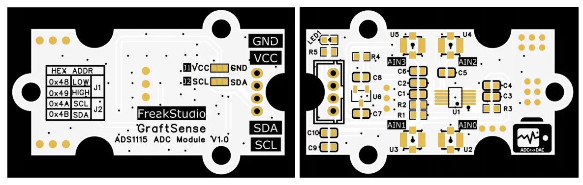
This module provides an I2C communication interface: it supports standard I2C communication rates, and the J1 and J2 headers can be used to configure the ADDR pins to control the I2C device address. Note that only one short-circuit point connection can be configured between J1 and J2; that is, the ADDR pin must be connected to exactly one of the 4 pins, and multiple selections are not allowed. This module can stably implement 16-bit high-precision AD conversion data transmission for 4-channel differential or 8-channel single-ended analog signals;The onboard input channel interface is IPEX1-4-TXZ 214, and an IPEX1 to DuPont wire adapter cable can be used to facilitate the connection of external analog signal sources such as sensors. It is suitable for scenarios including sensor signal acquisition for maker projects, analog quantity conversion for industrial inspection, and voltage monitoring of portable devices, providing the system with high-precision analog signal digital interaction capabilities.
3.3 Application Experiment
3.3.1 Experiment Preparation and Code Burning
Here, we use the GraftPort-RP2040 development board for testing, and connect the analog-to-digital conversion module based on the ADS1115 chip to communicate with the main controller via the I2C interface.
Here, we first use the HY2.0-4P cable to connect the module to the GraftPort-RP2040 development board's I2C0 interface, then use the IPEX to MCX adapter cable to connect the module's AIN0 input to the signal output interface DDS of the handheld signal generator:
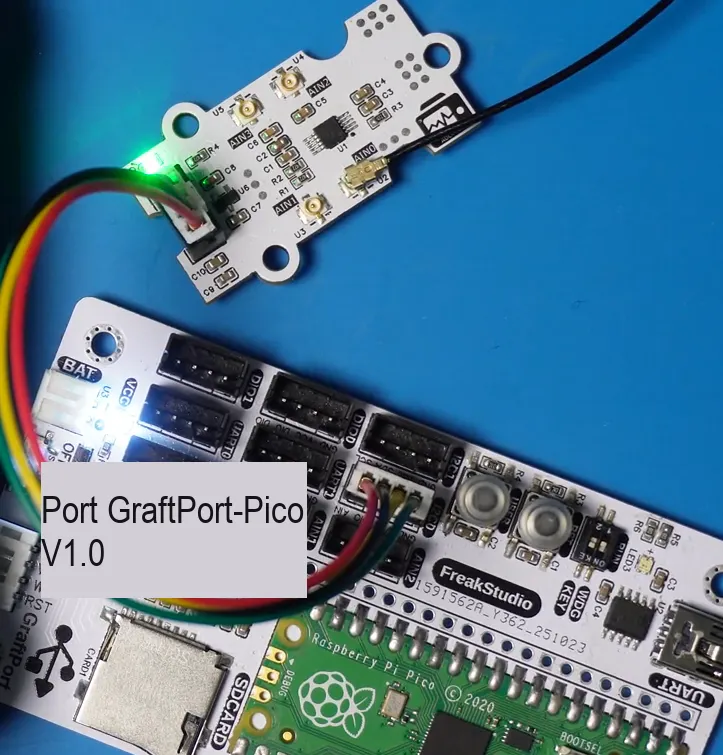
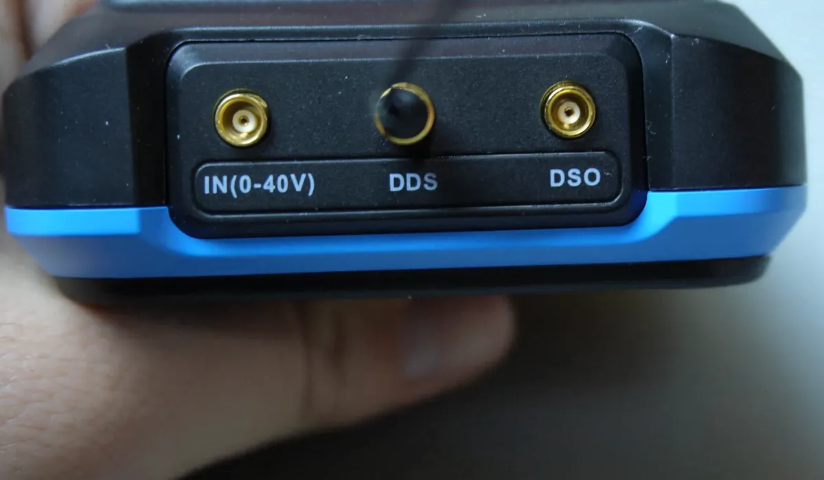
The module connections are shown in the following table:
Development Board Pins | Module Pins | Description |
Pin 4 |
| I2C data transmission line, corresponding to |
Pin 5 |
| I2C clock signal line, corresponding to |
- |
|
|
Here, we need to search for the relevant driver packages on uPyPI: https://upypi.net/zh/
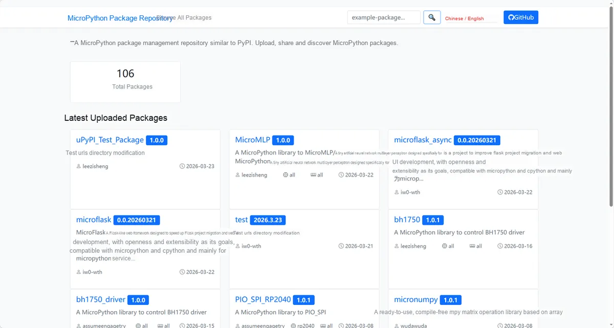
Enter ads1115_driver to search, and the following will be displayed:

Click to copy the local installation command:
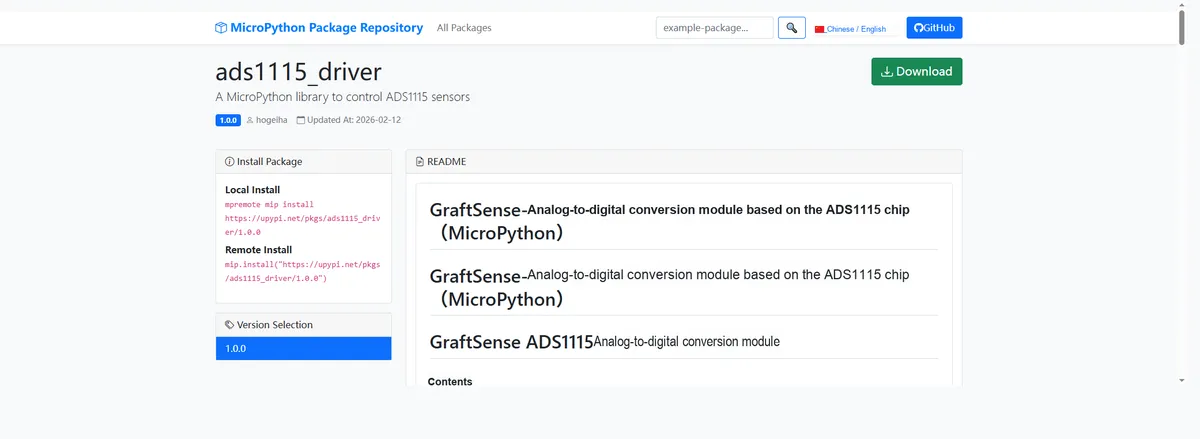
Here, we can import the module driver library code via the mip tool. Below are the usage commands for the mpremote tool:
mpremote mip install github:FreakStudioCN/GraftSense-Drivers-MicroPython/signal_acquisition/ads1115_driverImport the ADC module based on the ADS1115 chip - MicroPython driver code, then copy the following main.py code into our project:
# Python env   : MicroPython v1.23.0
# -*- coding: utf-8 -*-
# @Time    : 2024/10/7 2:21 PM
# @Author  : Li Qingshui
# @File    : main.py
# @Description : ADC experiment: use the external ADS1115 ADC chip to collect data, with sampling triggered by a timer

# ======================================== Import Modules ========================================

# Import hardware-related modules
from machine import Pin, I2C, Timer, UART
# Import time-related modules
import time
# Import the external ADC module
from ads1115 import ADS1115
# Import the module for packing and unpacking binary data and native data types
import struct

# ======================================== Global Variables ============================================

# External ADC address
ADC_ADDRESS = 0
# Channel the rotary potentiometer is connected to: AIN0
POT_CHANNEL = 0

# Variables for the moving average filter
FILTER_SIZE   = 20
filter_buffer = []
filter_sum = 0

# ======================================== Functions ============================================

# Define the timer callback function
def timer_callback(timer):
    """
    Timer callback function, used for periodic sampling
    Args:
        timer (machine.Timer): Timer object.

    Returns:
        None

    ==========================================

    Timer callback function for periodic sampling.

    Args:
        timer (machine.Timer): Timer object.

    Returns:
        None

    """
    # Declare global variables
    global adc, POT_CHANNEL, FILTER_SIZE

    # Collect data
    try:
        # Set the current conversion rate and channel
        adc.set_conv(rate=7, channel1=POT_CHANNEL)
        # Read the sampled data and start the next conversion
        raw_adc = adc.read_rev()
        # Convert the raw value to voltage
        voltage = adc.raw_to_v(raw_adc)
        # Print the sampled data
        print(f"Channel AIN{POT_CHANNEL}: {voltage:.4f} V (Raw: {raw_adc})")
        # Store the raw ADC value as int16
        adc_value = int(raw_adc)
        # Use a separate moving average filter function
        average = moving_average_filter(adc_value, FILTER_SIZE)

        # Build and send the data frame, passing the raw value and the filtered value
        send_data_frames(raw_adc, average)
    except Exception as e:
        print("Error in timer_callback:", e)

# Serial data frame packing function
def send_data_frames(raw_adc, average):
    """
    Serial data send function, sends the raw ADC value and the filtered average value

    Args:
        raw_adc (int): Raw value collected by the ADC.
        average (int): Filtered average value.

    Returns:
        None

    ==========================================

    UART data transmission function, sends raw ADC value and filtered average value.

    Args:
        raw_adc (int): Raw ADC collected value.
        average (int): Filtered average value.

    Returns:
        None

    """
    global uart

    try:
        # Build the data frame
        # The frame header is 0xAA 0xBB, followed by two 16-bit values in little-endian format
        frame_header = struct.pack('<2B', 0xAA, 0xBB)
        frame_data = struct.pack('<2H', raw_adc & 0xFFFF, average & 0xFFFF)
        frame_full = frame_header + frame_data
        # Send the data frame
        uart.write(frame_full)
    except Exception as e:
        print("Error in send_data_frames:", e)

# Moving average filter function
def moving_average_filter(new_value, filter_size):
    """
    Args:
        new_value (int): New sample value.
        filter_size (int): Filter window size.

    Returns:
        int: Current moving average.

    ==========================================

    Moving average filter.

    Args:
        new_value (int): New sampling value.
        filter_size (int): Filter window size.

    Returns:
        int: Current moving average.
    """
    # Declare global variables
    global filter_buffer, filter_sum

    # Add the new value to the buffer
    filter_buffer.append(new_value)
    filter_sum += new_value

    # If the buffer exceeds the filter size, remove the oldest value
    if len(filter_buffer) > filter_size:
        removed = filter_buffer.pop(0)
        filter_sum -= removed

    # Calculate and return the moving average
    return filter_sum // len(filter_buffer)

# ======================================== Custom Classes ============================================

# ======================================== Initialization ==========================================

# Power-on delay of 3 s
time.sleep(3)
# Print debug message
print("FreakStudio: Using ADS1115 acquire signal")

# Create a serial port object with the baud rate set to 256000
uart = UART(0, 256000)
# Initialize the uart object with a baud rate of 256000, 8 data bits, no parity, and 1 stop bit
# Set the receive pin to GPIO1 and the transmit pin to GPIO0
# Set the serial port timeout to 100ms
uart.init(baudrate  = 256000,
          bits      = 8,
          parity    = None,
          stop      = 1,
          tx        = 0,
          rx        = 1,
          timeout   = 100)

# Create a hardware I2C instance using the I2C0 peripheral, with a clock frequency of 400KHz, SDA pin 4, and SCL pin 5
i2c = I2C(id=0, sda=Pin(4), scl=Pin(5), freq=400000)

# Start scanning for devices on the I2C bus and return a list of slave addresses
devices_list = i2c.scan()
print('START I2C SCANNER')

# If devices_list is empty, no device is connected to the I2C bus
if len(devices_list) == 0:
    print("No i2c device !")
# If not empty, print the slave device addresses
else:
    print('i2c devices found:', len(devices_list))
    # Iterate over the slave device address list
    for device in devices_list:
        print("ADC I2C hexadecimal address: ", hex(device))
        ADC_ADDRESS = device

# Create the ADC instance with the gain set to 1
adc = ADS1115(i2c, ADC_ADDRESS, 1)

# Initialize the software timer with a period of 10 ms (100 Hz)
timer = Timer(-1)
timer.init(period=10, mode=Timer.PERIODIC, callback=timer_callback)

# ========================================  Main Program  ============================================

# Infinite loop: no specific operation
while True:
    # Delay 1s
    time.sleep(1)
This code is based on MicroPython and is a ADS1115 external ADC chip Data Acquisition program. It first initializes the UART serial port (baud rate 256000) and I2C bus (scans the ADS1115 device address). After creating an ADS1115 instance, it triggers timed acquisition via a software timer with a 10ms period, reads the raw AIN0 channel's rotary potentiometer raw ADC value, converts it to a voltage value and prints it, then processes the raw value with a sliding mean filter with a window size of 20. Finally, it packages the raw value and filtered value into a data frame in the specified format and sends it via the serial port; the main loop only performs a 1-second delay wait.
3.3.2 View via SerialPlot Serial Port Plotter
Before flashing the code, we need to complete the configuration of SerialPlot serial plotter.
- Configure serial port parameters: On the
Porttab, select the correct serial port (e. g.COM5), set the baud rate to 256000, data bits to 8, stop bits to 1, and no parity bit. - Click "Open": After confirming the configuration is correct, click the "
Open" button in the upper right corner to open the serial port

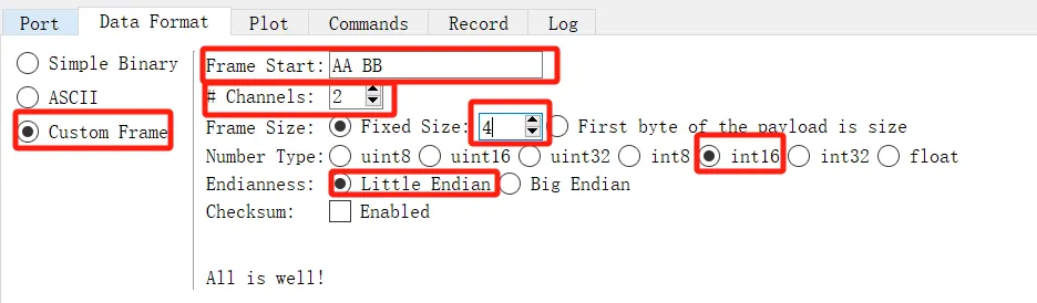
- Select the data format: switch to the
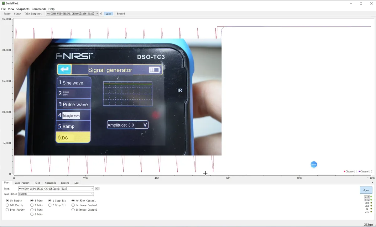
Data Formattab, select the"Custom Frame"format, set the frame headers to0xAAand0xBB, and set the number of channels to 2. Since we are transmitting two 16-bitADCdata values, and oneADCdata value occupies two bytes, set theFrame Sizehere to a fixed 4 bytes, set the data type to 16-bit signed number, and select little-endian at the same time
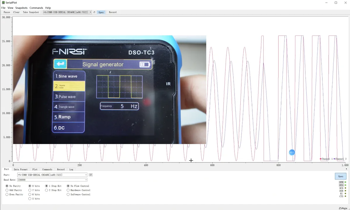
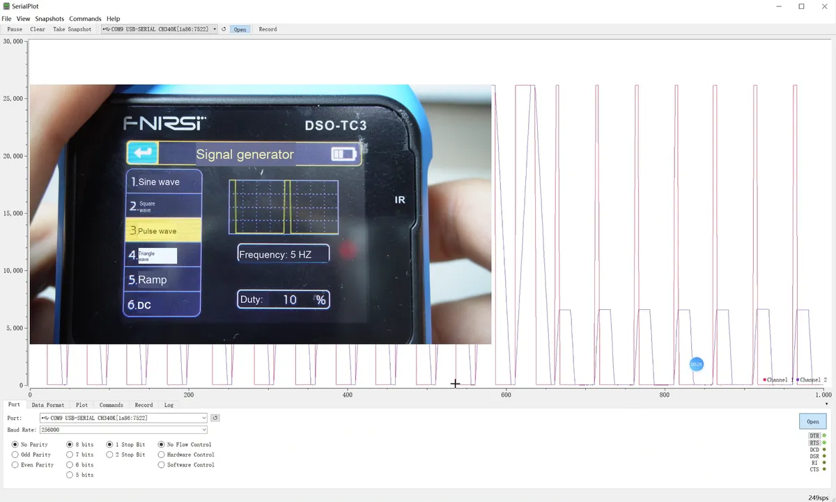
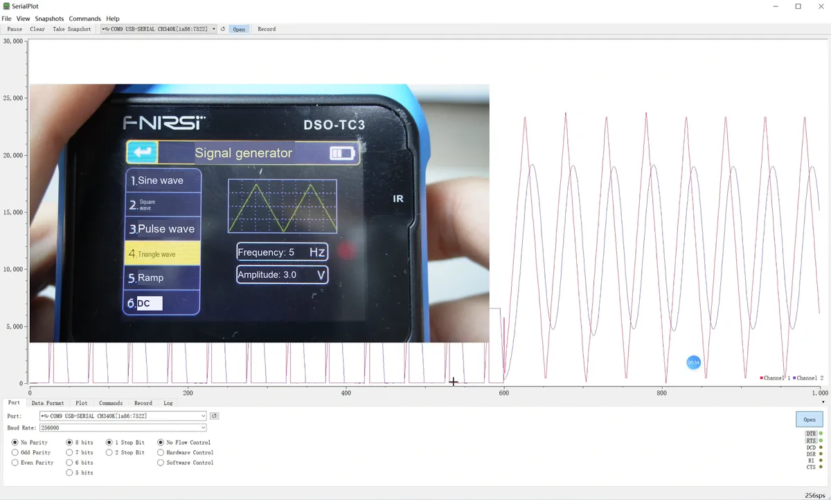
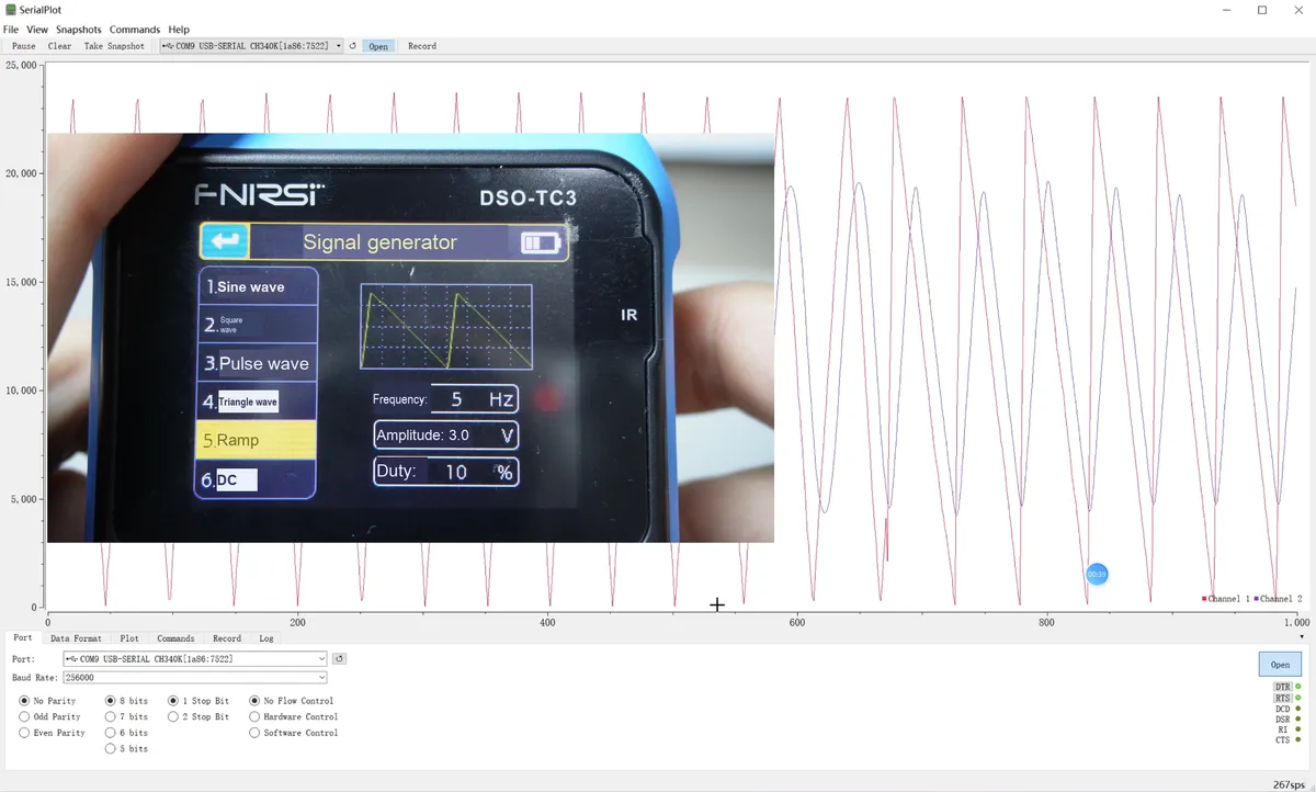
As we adjust different waveforms, the corresponding sampled waveforms also change:
3.3.3 Thonny Serial Plotter View
To facilitate testing, you can directly view the printed waveforms of voltage and raw ADC values in the plotter of the Thonny terminal to intuitively observe the changes of unfiltered acquisition data; to view the filtered data, you need to connect the MiniUSB cable to the UART1 interface on the development board, and receive the data packet containing the raw values and filtered values sent by the serial port, so as to obtain the filtered ADC data.
Burn the code, then open the Thonny serial plotter:
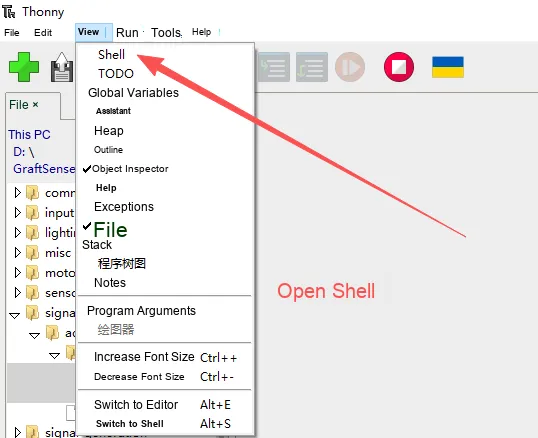
Check the option under the "View" menu Shell
Right-click on the blank area of the Shell interface and select "Show Plotter"
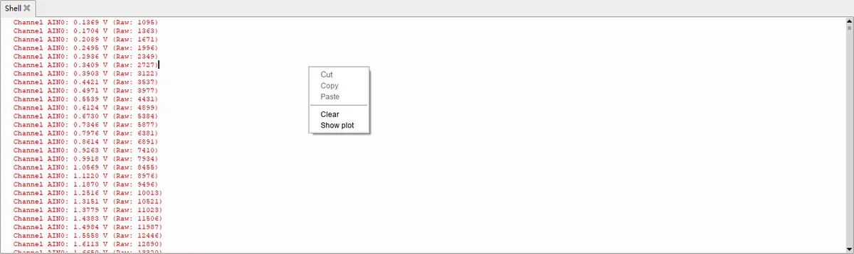
Run the code, and the serial plotter will draw the original output. The output is as follows:
November 21 (3).mp4 8.0 MB
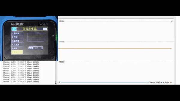
According to the plotter data from the hardware connection and Thonny terminal in the figure, ADS1115 external ADC has successfully collected the AIN0 channel signal. Meanwhile, the program's functions of timed acquisition and data printing work properly, the hardware connection is adapted to the software logic, and the collected data is reliable.
IV. Drivers
ads1115_driver.zip 10 KB
5. BOM & Recommended Alternative Parts
None.
VI. Revision History
Document Version | Date of Revision | Modifier | Modified Content |
v1.0 | 2025-11-14 | Ling Gaoxing | Initialize the document |
v1.1 | 2025-12-29 | Li Zisheng | Added application experiments and production files |
v1.2 | 2025-12-31 | Xin Ruili | Create an open version of the document based on the internal document version v1.1. |
v1.3 | 2026-03-29 | Xin Ruili | Modified the application experiment section |
VII. Relevant Materials
7.1 Chip Datasheet
ads1115.pdf 2.0 MB
7.2 Unique Icons for PCB Silkscreen