Contents
- I. Module Introduction
- II. Introduction to Main Chips
- 2.1 Chip Overview
- 2.2 Pin Definition
- 2.3 Functional Block Diagram
- 2.4 Performance Parameters
- 2.5 Reference Circuit
- 2.6 Chip Configuration
- 2.7 Communication Interfaces and Related Protocols
- 2.8 PCB Routing Precautions
- III. Instructions for Circuit Engineering and Module Usage
- 3.1 Circuit Source Engineering
- 3.2 Module Usage Instructions
- 3.3 Application Experiment
- IV. Drivers
- 5. BOM & Recommended Alternative Parts
- VI. Revision History
- VII. Relevant Materials
- 7.1 Chip Datasheet
- 7.2 Unique Icons for PCB Silk Screen
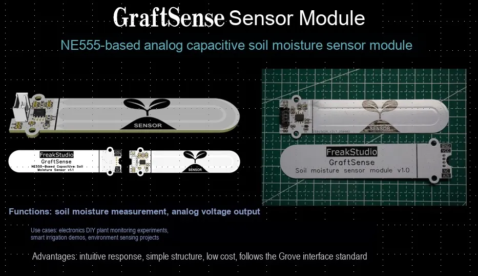
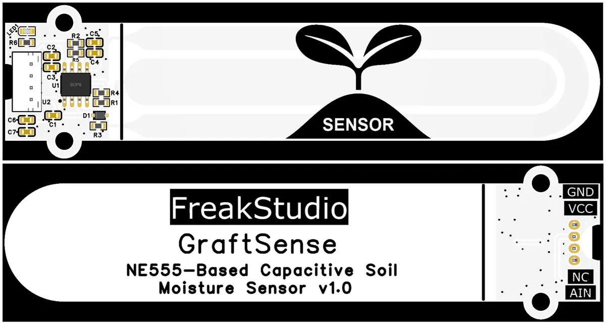
I. Module Introduction
NE555-based Analog Capacitive Soil Moisture Sensor Module, with the NE555 timer as the core, detects soil moisture via the capacitive principle and outputs analog signals through the AIN interface for collection by the MCU ADC. Equipped with auxiliary circuits including power indication and filtering, it is suitable for soil moisture monitoring in scenarios such as agriculture and green plant cultivation, serving as a low-cost, easy-to-integrate maker-grade sensor solution.
II. Introduction to Main Chips
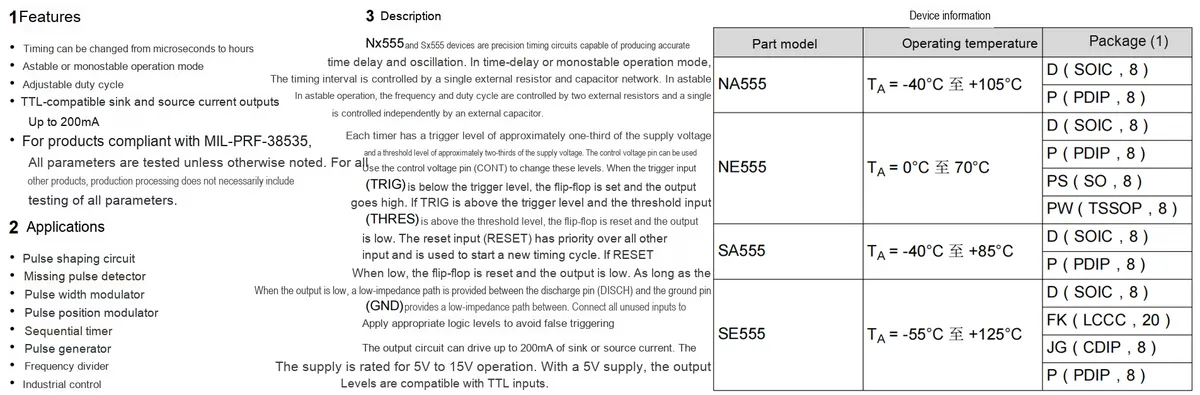
2.1 Chip Overview
2.2 Pin Definition
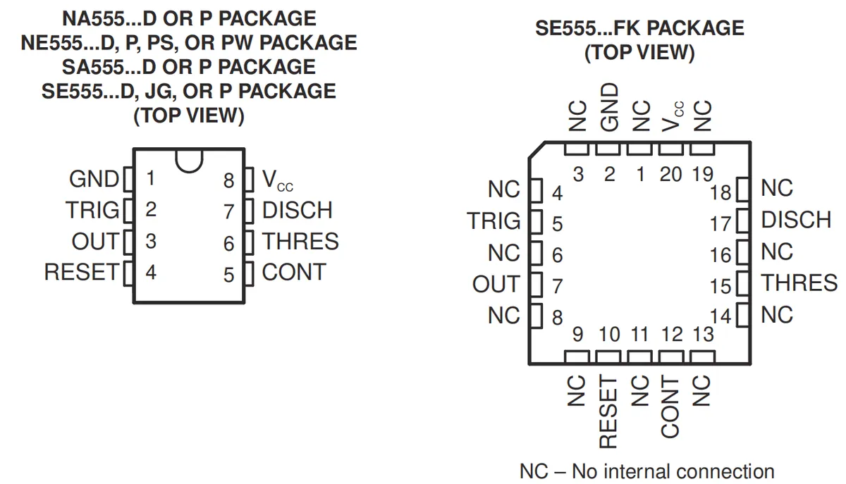
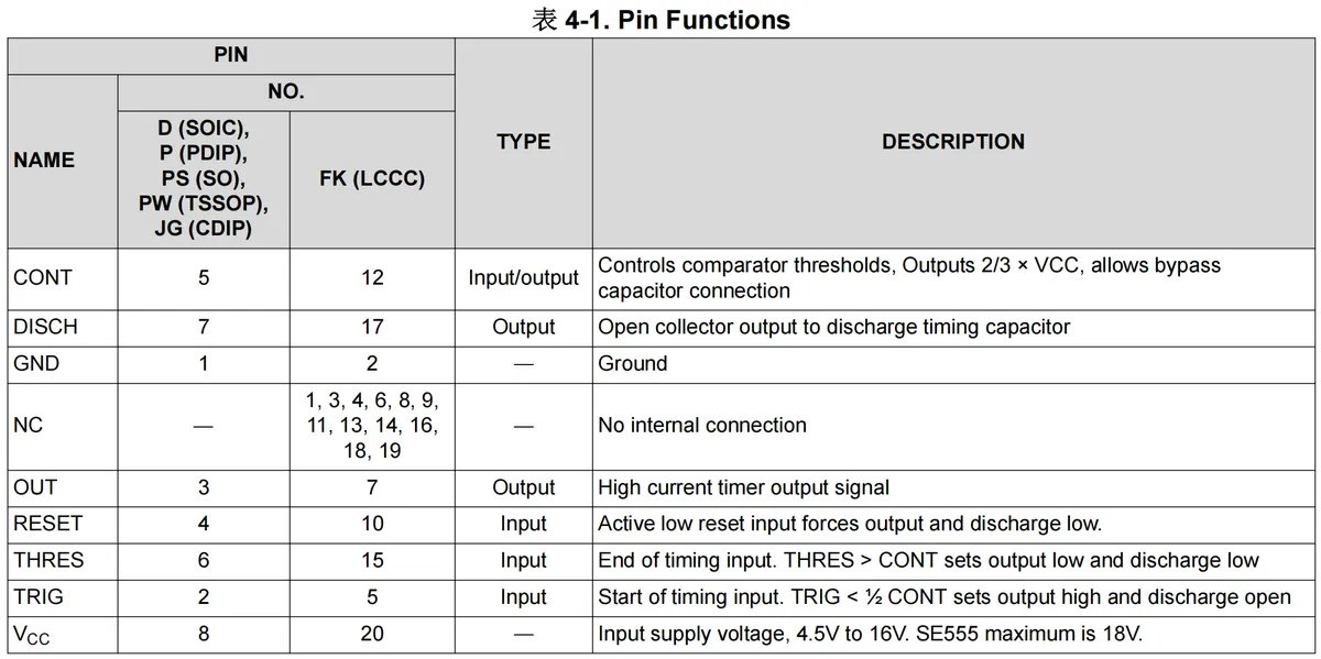
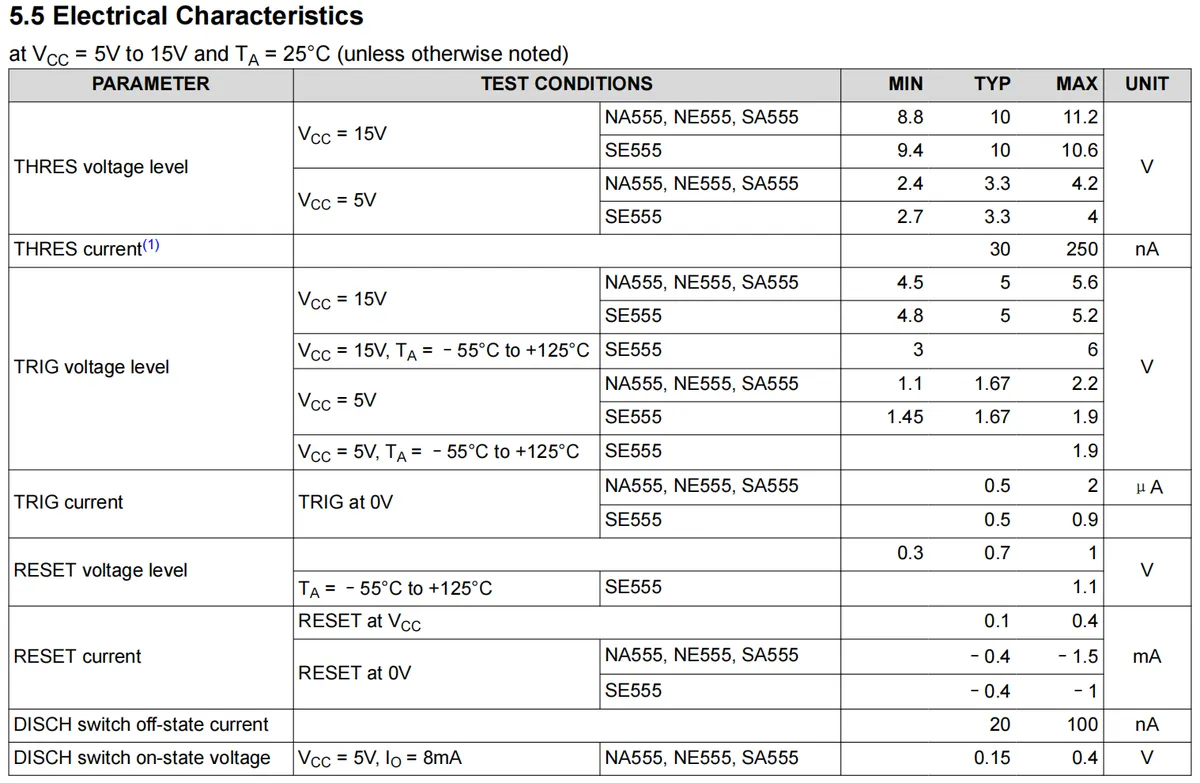
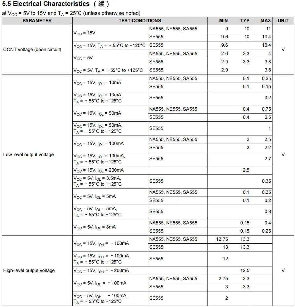
CONT(Pin 5): Input/output type, used to control the comparator threshold, output2/3×VCC, and supports bypass capacitor connection.DISCH(Pin 7): Output type, open-collector output, responsible for discharging the timing capacitor.GND(Pin 1): Ground pin, providing the reference ground for the circuit.NC: Pin with no internal connection (see the table for pin numbers corresponding to different packages).OUT(Pin 3): Output type, providing a high-current timer output signal.RESET(Pin 4): Input type, active-low reset input that forces the output and discharge terminal to a low level.THRES(Pin 6): Input type, end-of-timing input. When the voltage atTHRESis greater than the voltage atCONT, the output and discharge terminal are set low.TRIG(Pin 2): Input type, timing start input. When theTRIGvoltage is less than½ CONTvoltage, the output is set high and the discharge terminal is open-circuited.VCC(Pin 8): Power supply input pin, with a supply voltage range of 4.5V to 16V (SE555: max 18V).
2.3 Functional Block Diagram
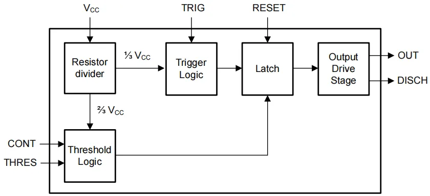
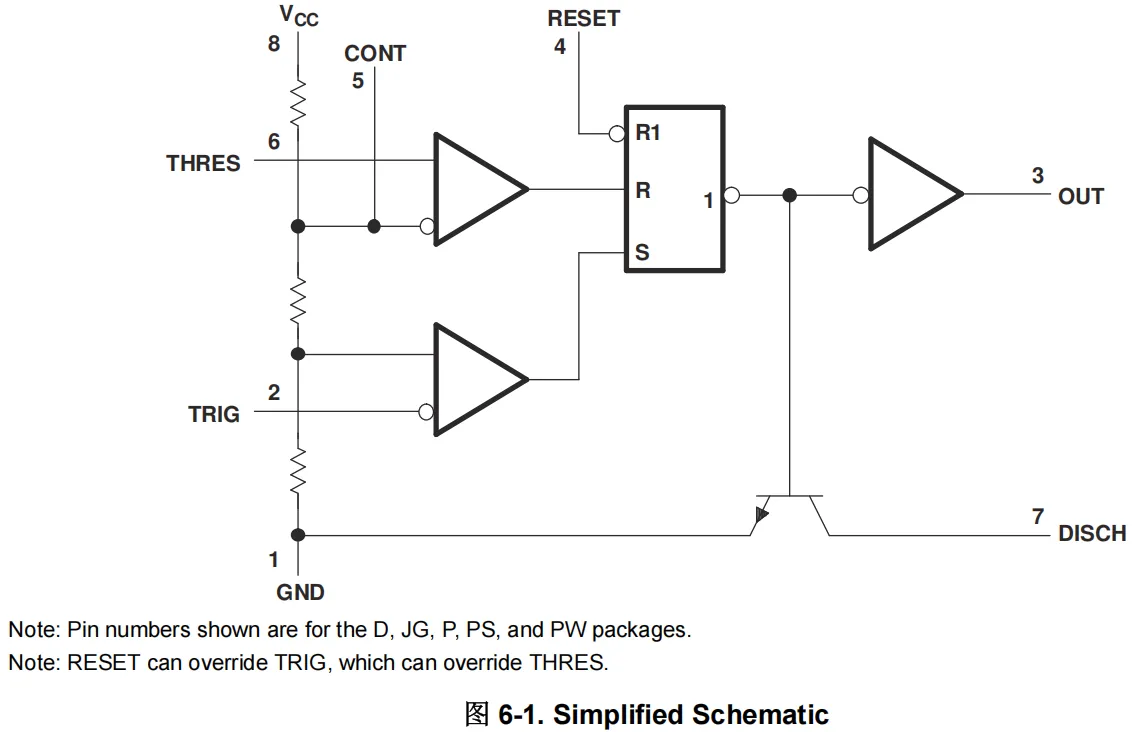
This block diagram illustrates the internal structure of Nx555 / Sx555, which mainly consists of the following units:
- Resistive voltage divider: Consists of three series-connected resistors, generating reference voltages of
2/3×VCCand1/3×VCCto provide thresholds for the comparator. - Two comparators: a threshold comparator (which processes the input of the
THRESpin and compares it with2/3×VCC) and a trigger comparator (which processes the input of theTRIGpin and compares it with1/3×VCC), whose outputs control theRSflip-flop. RSflip-flop: determines the state according to the output of the comparator, and then controls the output and the discharge circuit.- Discharge transistor: controls the on-off of
DISCHpin to realize the charging and discharging of the external capacitor. - Output Buffer: Enhances
the driving capability of the OUTpin and outputs high/low level signals. RESETPin: Active low, which can force the flip-flop to reset and set the output to low level.
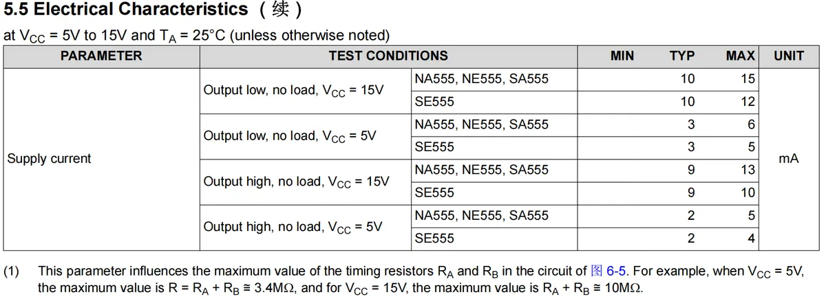
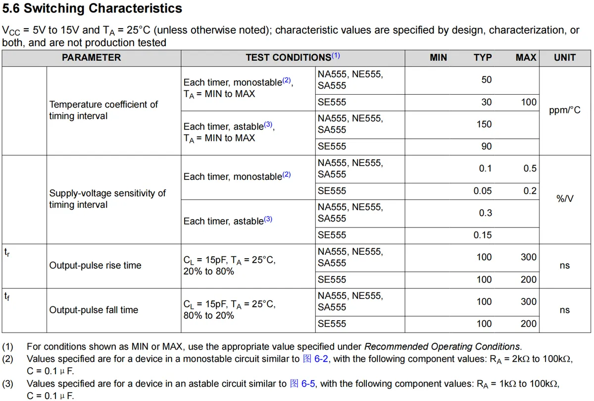
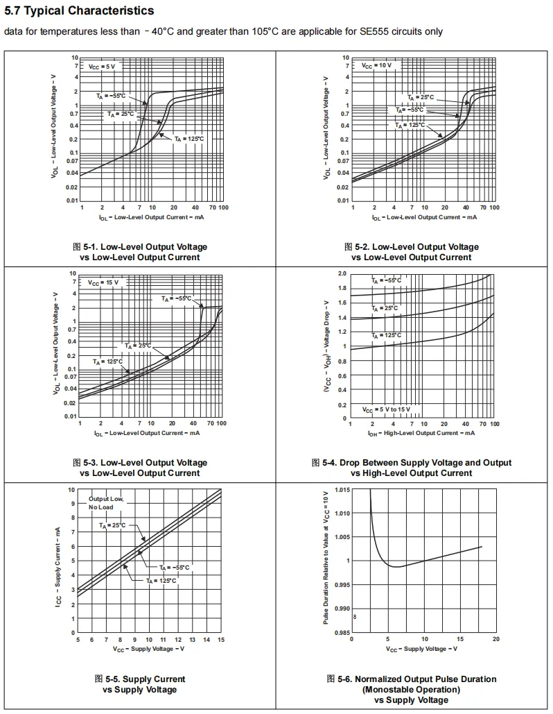
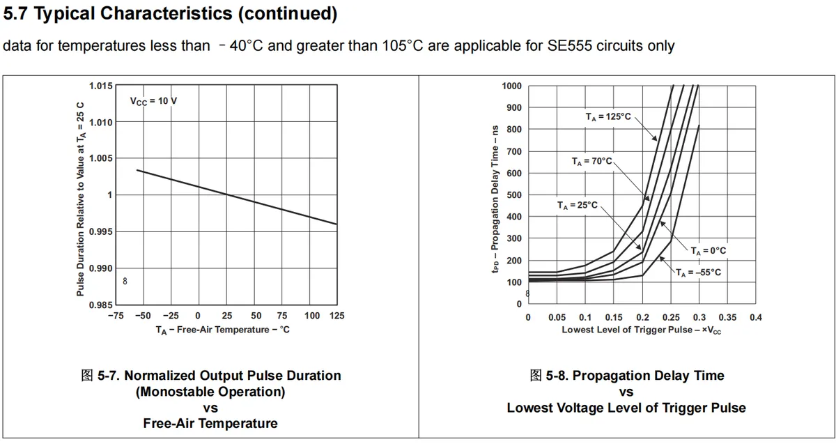
2.4 Performance Parameters
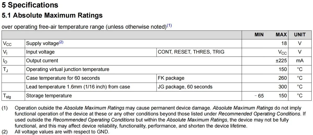
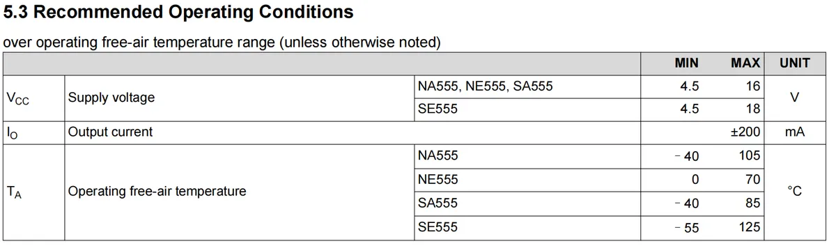
- Supply Voltage (
Vcc): Max. 18V; - Input voltage (
CONT,RESET,THRES,TRIGpins): max.Vcc; - Output current (
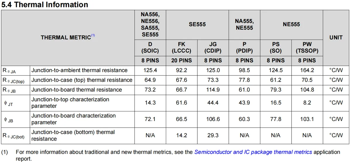
Io):±225mA; - Junction Operating Temperature (
Tj): 150°C; FKPackage case temperature (60 seconds): 260°C;JGPackage pin temperature (1.6mm from the housing, 60 seconds): 300°C;- Storage temperature (
Tstg):-65°C to 150°C.

The electrostatic discharge (V₍ₑₛₙ₎) ratings of this chip are as follows: ±500V for the human body model (HBM)(compliant with the ANSI / ESDA / JEDEC JS-001 standard), and ±1500V for the charged device model (CDM)(compliant with the ANSI / ESDA / JEDEC JS-002 standard).
2.5 Reference Circuit
2.5.1 Pulse Missing Detector
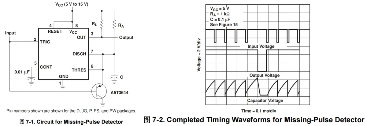
NE555 pulse loss detector is based on a monostable circuit, which continuously retriggers the timing interval via the input pulse train; when the pulse interval is too long or a pulse is missing, the timing interval elapses and an alarm pulse is output. In the design, R_A and C are selected such that R_A×C is greater than the maximum normal input high-level duration, which enables detection of pulse loss or abnormal intervals in the pulse train, making it suitable for pulse sequence fault detection scenarios.
2.5.2 Pulse Width Modulation
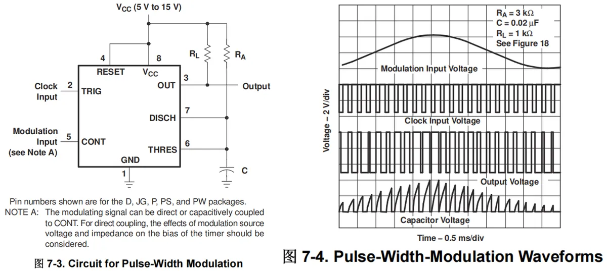
NE555 Pulse Width Modulation (PWM) circuit triggers the monostable operating mode via the clock input, and the modulation signal input to the CONT pin alters the internal threshold voltage, thereby realizing the modulation of the output pulse width; the typical waveforms illustrate the relationship among the modulation input voltage, clock input voltage, output voltage and capacitor voltage, which is applicable to scenarios such as motor control and signal modulation.
2.5.3 Pulse Position Modulation
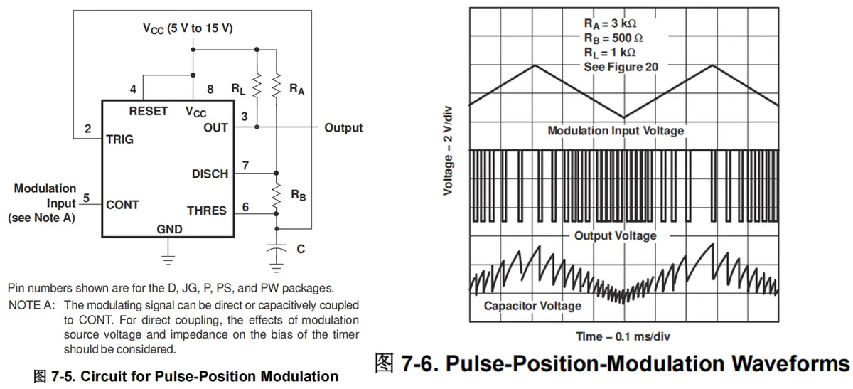
NE555 pulse position modulation circuit inputs a modulation signal to the CONT pin to change the internal threshold voltage, thereby modulating the Time Lag of the free-running oscillator to realize pulse position modulation; during design, the astable mode formula can be referred to for determining the frequency and duty cycle, the modulation signal can be any waveform such as a triangular wave, and the typical waveform shows the relationship among the modulation input, output voltage and capacitor voltage, which is applicable to scenarios such as signal modulation.
2.5.4 Sequential Timer
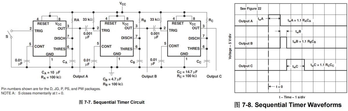
NE555 sequential timer is constructed by cascading multiple monostable circuits, which uses a 33kΩ resistor and a 0.001μF capacitor to transmit the start pulse; the pulse width of each timer is calculated via tw = 1.1×R×C to realize sequential triggering of output signals. It is applicable to scenarios such as system startup initialization and sequential activation of test signals, and its typical circuit and waveforms demonstrate the effect of multi-channel sequential timing.
2.6 Chip Configuration
2.6.1 Monostable Mode
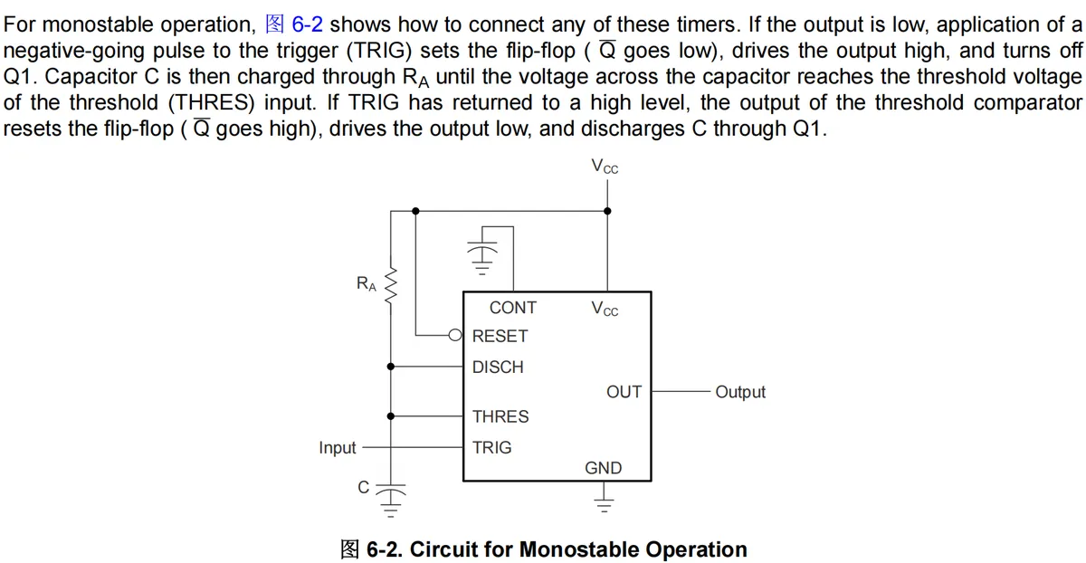
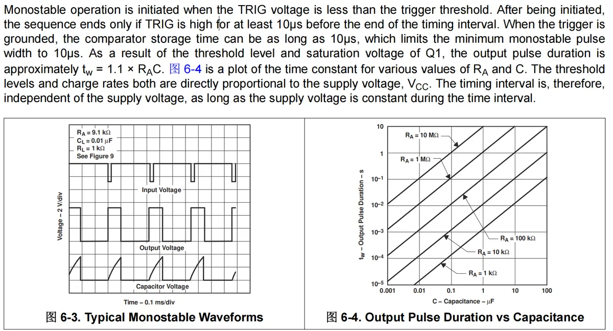
The NE555 in monostable mode is triggered by a negative pulse at the TRIG pin; the output goes high after the capacitor charges, and switches low when the voltage reaches the threshold. The pulse width is approximately 1.1×R×C, making it suitable for single-pulse timing applications.
2.6.2 Astable Mode
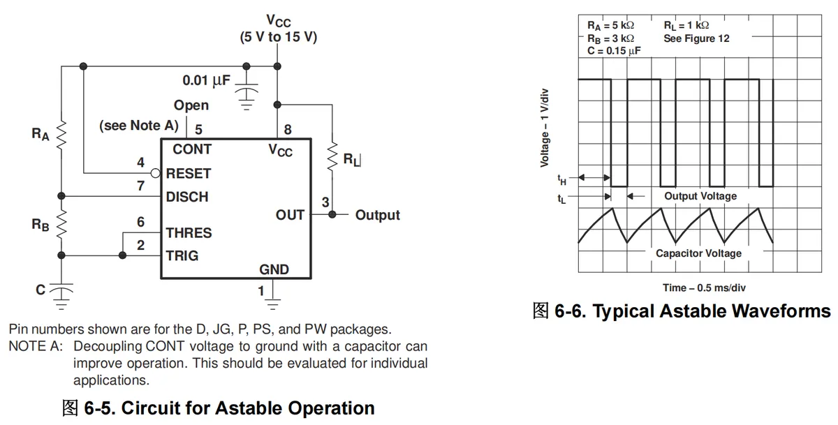
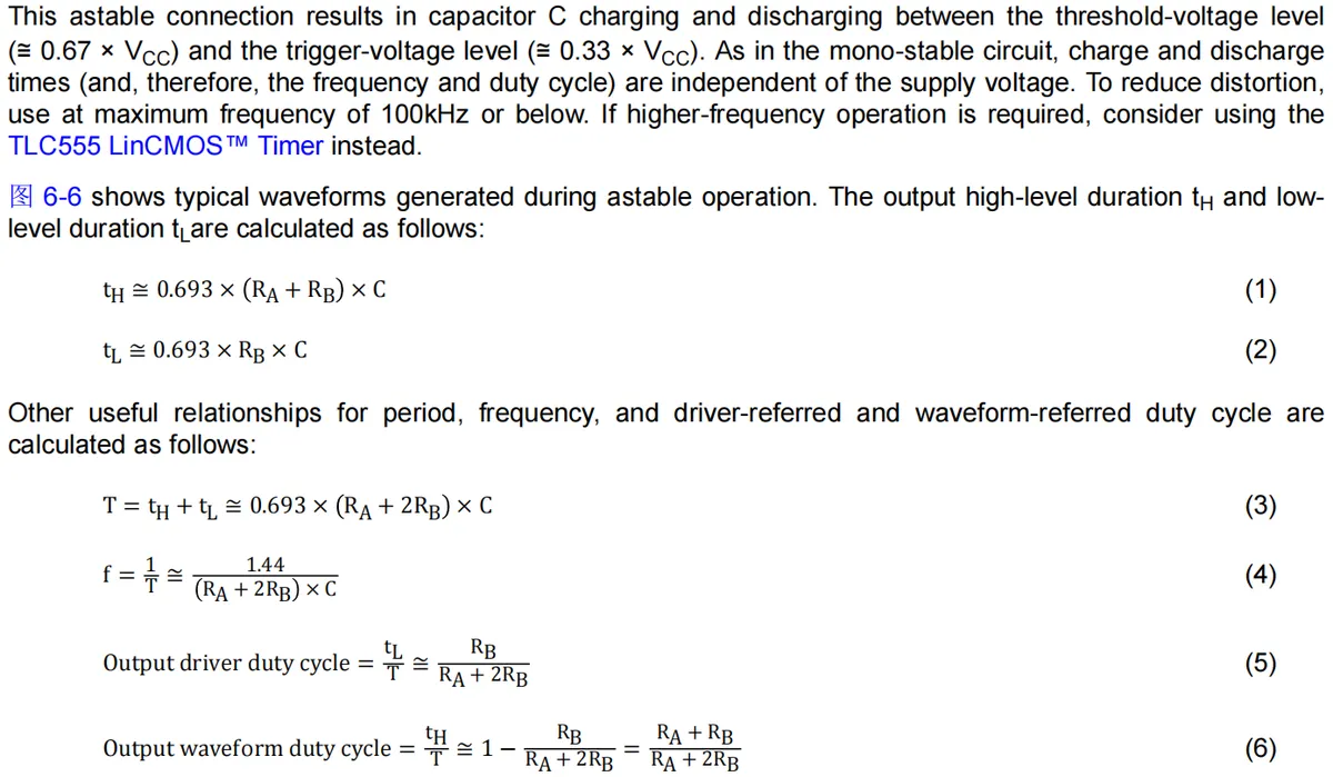
NE555 in astable mode forms a charging and discharging network through resistors RA, RB and capacitor C, which enables the capacitor to charge and discharge cyclically between 0.33× VCC and 0.67× VCC, outputting a continuous square wave; its period is approximately 0.693×(RA + 2 RB)× C, the frequency is approximately 1.44/[(RA + 2 RB)× C], and the duty cycle is independently controlled by RA and RB, making it suitable for scenarios such as square wave generation and PWM.
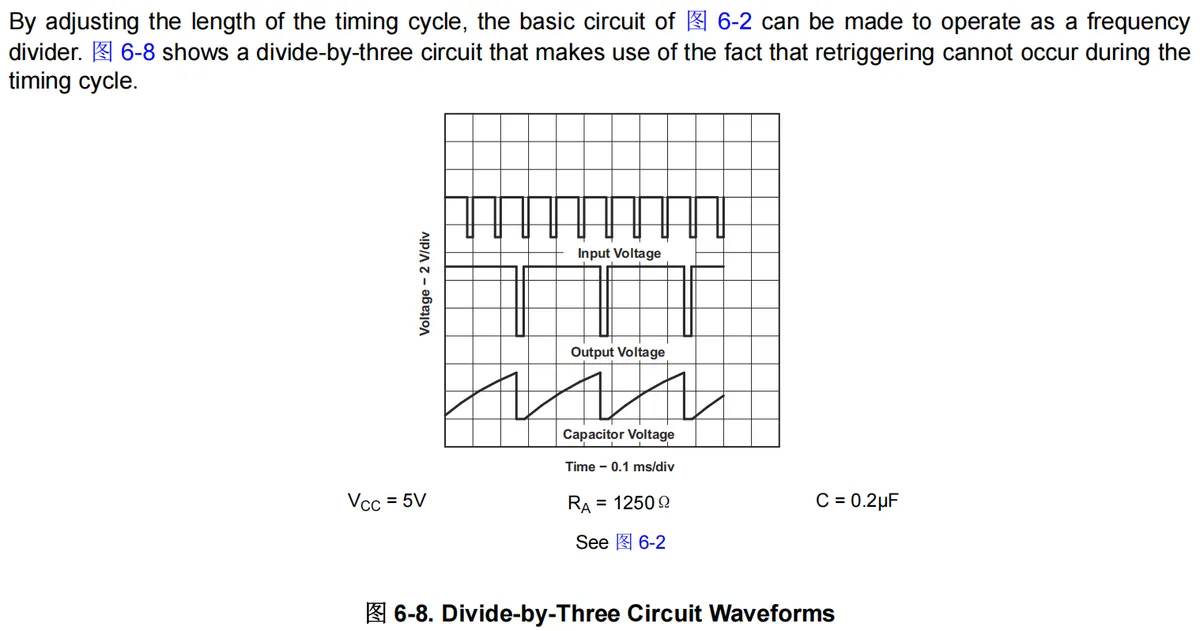
2.6.3 Frequency Divider Mode
By adjusting the timing period, the basic NE555 circuit can function as a frequency divider. The diagram below illustrates the waveforms of a 1/3 frequency divider circuit, which achieves 1/3 frequency division of the input signal by utilizing the characteristic that retriggering is not possible within a timing period. The parameters are as follows: Vcc = 5V, RA = 1250Ω, C = 0.2μF.
2.7 Communication Interfaces and Related Protocols
None.
2.8 PCB Routing Precautions

The Nx555 and Sx555 precision timers have a supply voltage range of 4.5V to 16V (the SE555 has a range of 4.5V to 18V). It is recommended to connect a 0.1μF ceramic bypass capacitor in parallel between Vcc and ground to filter out noise.
III. Instructions for Circuit Engineering and Module Usage
3.1 Circuit Source Engineering
To obtain the source code of the circuit, please follow the official account [Freak Embedded]
3.2 Module Usage Instructions
The schematic diagram of this module is shown below:
SCH_Analog Capacitive Soil Moisture Sensor Module Based on NE555_v1.0_2025-11-24.pdf 2.0 MB
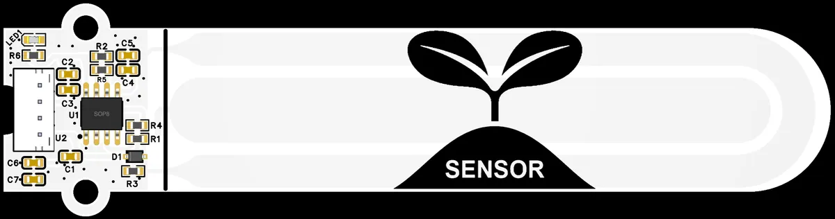
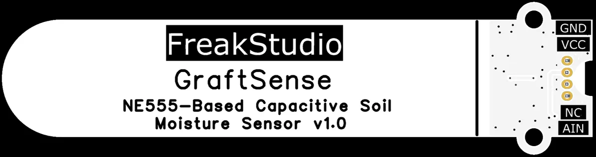
This module provides an analog output interface AIN: which needs to be connected to the MCU ADC peripheral; through this interface, the analog voltage signal corresponding to soil moisture can be obtained. The core NE555 circuit of the module will adjust the operating characteristics of the circuit according to the soil moisture (changes in soil moisture will alter the equivalent capacitance value of the PCB capacitive wire), finally convert the moisture information into a continuously varying voltage signal, which is output via the AIN interface.
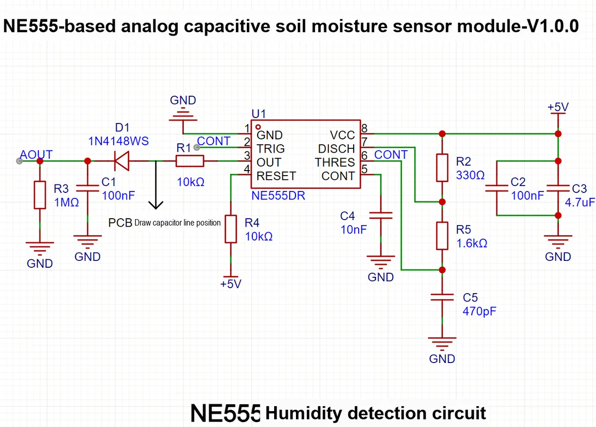
This schematic uses NE555 (U1) as the core to form a soil moisture detection circuit: the module is powered by 5V, C2 and C3 are power filter capacitors to stabilize the power supply;PCB printed capacitor lines act as moisture-sensitive elements, whose equivalent capacitance varies with soil moisture; this capacitor, together with R2, R5, C5 and other components, forms the charging and discharging network of NE555; changes in moisture will alter the charging and discharging cycle, thereby modifying the operating signal characteristics of NE555;The output signal of NE555 is conditioned via D1 (a 1N4148 diode), C1 and R3, then outputs an analog voltage signal corresponding to soil moisture from the AIN interface. Meanwhile, R4 pulls up the RESET pin of NE555 to keep it operating normally, ultimately realizing the conversion of " soil moisture → capacitance change → voltage signal " for acquisition by the ADC.
3.3 Application Experiment
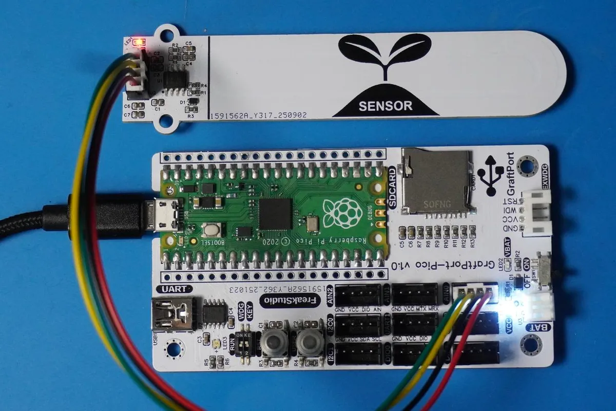
Here, we use the GraftPort-RP2040 development board for testing, and connect the NE555-based analog capacitive soil moisture sensor module to communicate with the main controller via the AIN interface.
Here, we first use the HY2.0-4P connection cable to connect the module to the GraftPort-RP2040 development board's AIN0 interface:
The module connections are shown in the following table:
Development Board Pins | Module Pins | Description |
Pin 26 |
| Analog signal input pin of the sensor chip on the MCU |
Pin 19 |
| - |
Here, we need to search for relevant driver packages on uPyPI: https://upypi.net/zh/
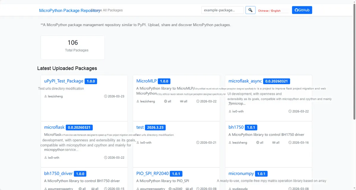
Enter soil_moisture_driver to search, and the following will be displayed:

Click to copy the local installation command:
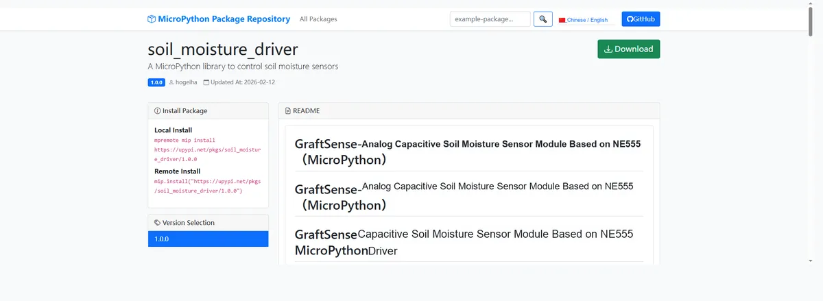
Here, we can use the mip tool to import module driver library code. Below are the usage commands for the mpremote tool:
mpremote mip install github:FreakStudioCN/GraftSense-Drivers-MicroPython/sensors/soil_moisture_driverAfter importing the analog capacitive soil moisture sensor module based on NE555 - MicroPython test code, copy the following main.py code into our project:
# Python env   : MicroPython v1.23.0
# -*- coding: utf-8 -*-
# @Time    : 2025/8/22 PM 12:49
# @Author  : 缪贵成
# @File    : main.py
# @Description : Capacitive soil moisture sensor test file

# ======================================== Import Modules =========================================

import time
from soil_moisture import SoilMoistureSensor

# ======================================== Global Variables =============================================

# ======================================== Functions =============================================

# ======================================== Custom Classes =============================================

# ======================================== Initialization configuration ===========================================

time.sleep(3)
print("FreakStudio: SoilMoistureSensor Test Start")
print("Please prepare the sensor for calibration (dry and wet)...")

# Initialize the sensor (e.g., ADC pin 26)
sensor = SoilMoistureSensor(pin=26)
print("Sensor initialized on ADC pin 26")

# ======================================== Main Program ===============================================

# Step 1: Calibrate the dry value
input("Place sensor in DRY air/soil and press Enter...")
dry_value = sensor.calibrate_dry()
print("Calibrated dry value:", dry_value)

# Step 2: Calibrate the wet value
input("Place sensor in WATER (fully wet) and press Enter...")
wet_value = sensor.calibrate_wet()
print("Calibrated wet value:", wet_value)

# Step 3: Set the calibration values
sensor.set_calibration(dry_value, wet_value)
print("Calibration set: dry={}, wet={}".format(dry_value, wet_value))

# Step 4: Read sensor data in a loop
print("\nCalibration completed. Start reading moisture...\n")
try:
    while True:
        raw = sensor.read_raw()
        moisture_percent = sensor.read_moisture()
        level = sensor.get_level()

        print(
            "Raw ADC: {:>5} | Moisture: {:>5.1f}% | Level: {}".format(
                raw, moisture_percent, level
            )
        )
        time.sleep(2)

except KeyboardInterrupt:
    print("\nTest stopped by user.")

print("SoilMoistureSensor Test Completed")
Here we first initialize the sensor connected to ADC pin 26, then guide the user through the calibration process (obtaining the raw ADC values of the sensor in dry and fully humid environments respectively). After setting the calibration parameters, we repeatedly read the raw sensor ADC data, convert it to a humidity percentage, determine the humidity level, and continuously print out this information.
To flash the code, open a terminal and use the mpremote tool to connect to the main controller; the output is as follows:
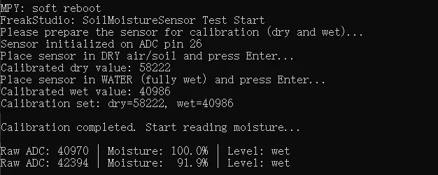
The following is the calibration procedure:
In the terminal interface, press ENTER when the sensor is in the air or in dry soil to start sampling the dry value:
In the terminal interface, press ENTER while the sensor is in moist soil to start sampling the moisture value:
Finally, after the calibration is completed, we insert the sensor module into the soil:
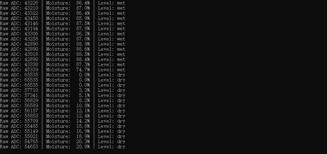
As can be seen from the terminal output, the sensor has completed calibration for the dry (58222) and fully wet (40986) states; the subsequently read raw ADC values are close to the fully wet calibration value, with corresponding humidity percentages of 100.0% and 91.9% respectively, and the humidity levels are both "wet", indicating that the current sensor is in a relatively humid environment, and meanwhile the sensor's functions of calibration, data reading and conversion all work properly.
IV. Drivers
5. BOM & Recommended Alternative Parts
None.
VI. Revision History
Document Version | Date of Revision | Modifier | Revised Content |
v1.0 | 2025-11-24 | Li Zisheng | Initialize the document The BOM sheet has not been finally checked, the driver has not been re-verified, and the 3.3 application experiment Not yet specified. |
v1.1 | 2025-12-29 | Li Zisheng | Added application experiments and production files |
v1.2 | 2025-12-31 | Xin Ruili | Create an open version of the document based on the internal document version v1.1. |
v1.3 | 2026-03-29 | Xin Ruili | Modified the application experiment section |
VII. Relevant Materials
7.1 Chip Datasheet
ne555.pdf 2.4 MB
C695838_555 Timer_NE555DR_Datasheet_WJ643770.PDF 517 KB
7.2 Unique Icons for PCB Silk Screen