Contents
- I. Module Introduction
- II. Introduction to Main Chips
- 2.1 Chip Overview
- 2.2 Pin Definition
- 2.3 Functional Block Diagram
- 2.4 Performance Parameters
- 2.5 Reference Circuit
- 2.6 Chip Configuration
- 2.7 Communication Interfaces and Related Protocols
- 2.8 PCB Routing Precautions
- III. Instructions for Circuit Engineering and Module Usage
- 3.1 Circuit Source Engineering
- 3.2 Module Usage Instructions
- 3.3 Application Experiment
- IV. Drivers
- 5. BOM & Recommended Alternative Parts
- VI. Revision History
- VII. Relevant Materials
- 7.1 Chip Datasheet
- 7.2 Unique Icons for PCB Silk Screen
I. Module Introduction
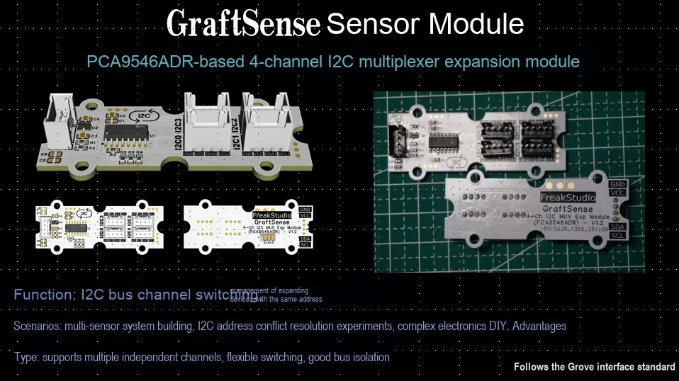
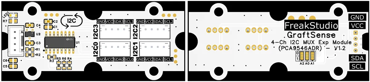
4-channel I2C Multiplexer Expansion Module Based on PCA9546ADR With the core adopting PCA9546ADR (a 4-channel TI I2C / SMBus switch chip), it supports switching from 1 master I2C to 4 slave I2C devices, solving the address conflict issue of I2C devices; the module integrates a DC-DC 5V-to-3.3V circuit (XC6209F332MR) to adapt to master controllers of different voltages, and is equipped with power filter capacitors and LED power indicators to ensure stable power supply;The chip address can be set via the A0 / A1 / A2 jumper caps to avoid multi-module conflicts; meanwhile, it is equipped with an MCU interface (connected to the main controller's I2C) and 4 sets of I2C expansion interfaces (for connecting external I2C devices). With a clear interface layout, it is suitable for embedded system designs that require expanding the number of I2C devices.
II. Introduction to Main Chips
2.1 Chip Overview
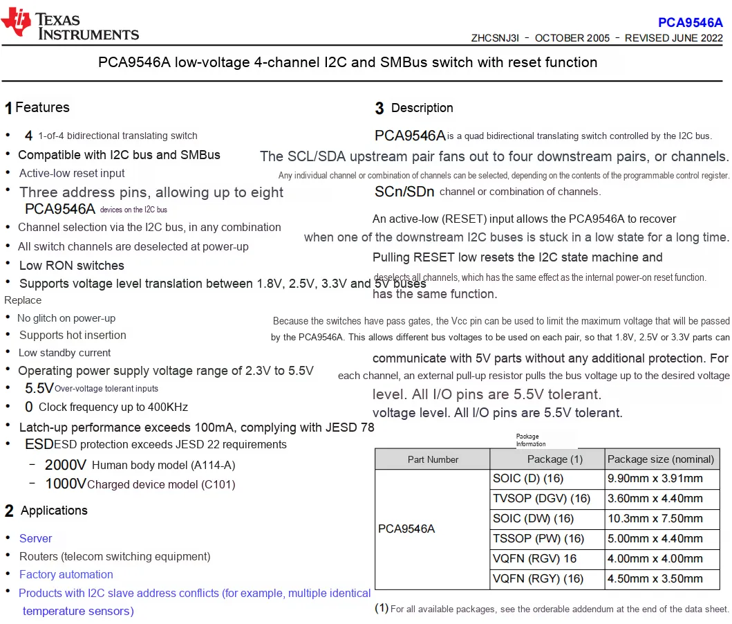
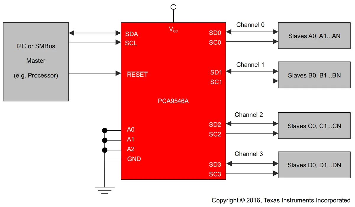
The previous block diagram illustrates the operating architecture of the 4-channel PCA9546A I2C / SMBus multiplexer: on the left is an I2C master device (e. g., a processor), whose SDA and SCL pins are connected to the corresponding pins of the PCA9546A, and the RESET pin is used to control the chip reset; the PCA9546A is powered via Vcc, its A0 / A1 / A2 address pins (grounded here) set its own I2C address, and GND is the ground terminal;The 4 channels on the right (Channel 0-3) respectively correspond to the SD (SDA) and SC (SCL) pins, and are connected to different groups of I2C slave devices (such as Slaves A0, B0, etc.).
The master device can control the PCA9546A via I2C commands to select and turn on a specific channel, thereby establishing communication with the slave device on that channel. This enables the switching connection between 1 master I2C bus and 4 groups of slave devices, solving the problem of I2C address conflict among multiple slave devices.
2.2 Pin Definition
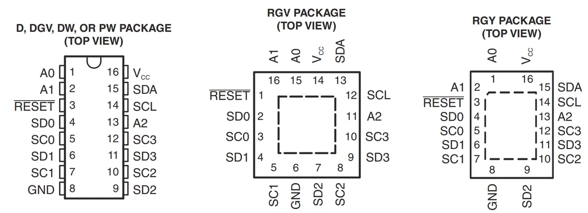
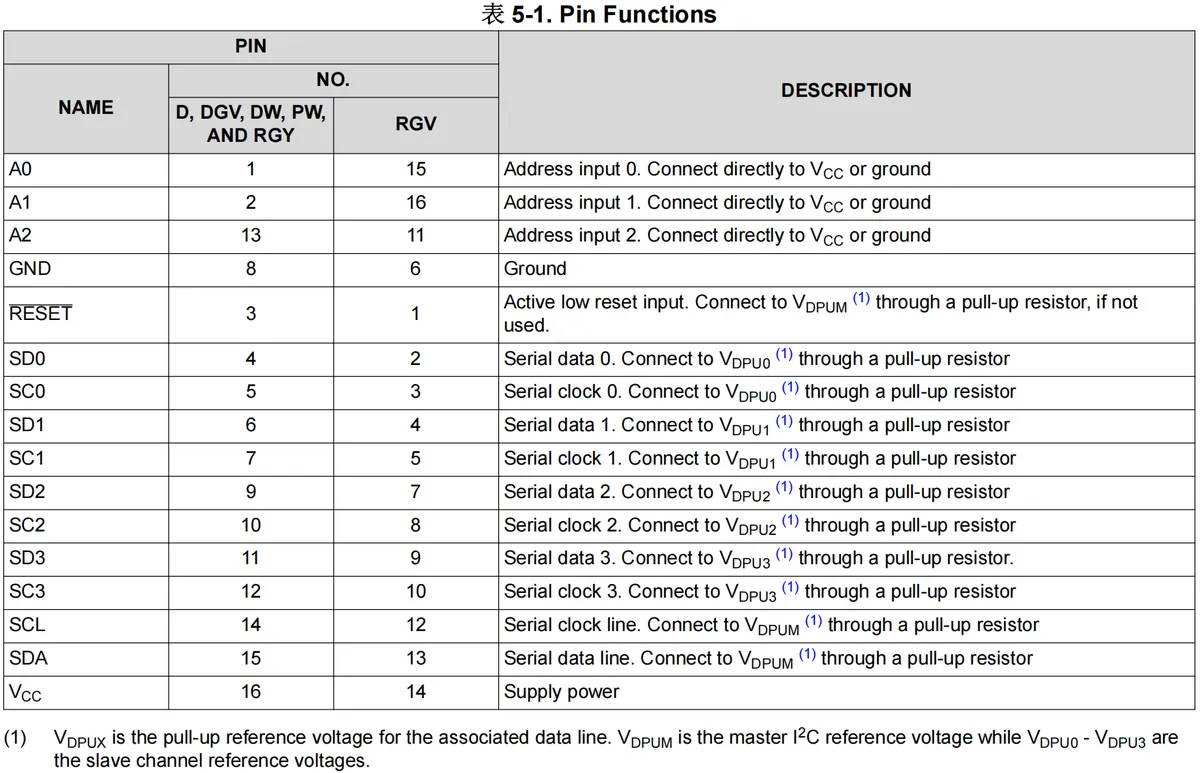
- Address pins:
A0,A1,A2, which configure the device's ownVcc/GNDvia connection toI2Caddress to prevent address conflicts among multiple modules; - Control Pin:
RESET(reset pin), active low, used to reset the channel selection status of the chip; - I2C bus pins :
SDAandSCLare I2C data/clock lines on the master device side;SD0/SC0~SD3/SC3are 4 channels corresponding to the slave device sideI2Cdata/clock lines, each group corresponding to a channel of slave device connection; - Power supply pins:
Vccis the power supply pin,GNDis the ground pin.
2.3 Functional Block Diagram
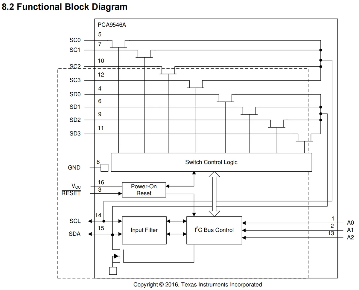
This is the functional block diagram of PCA9546A, which clearly illustrates its internal modules and signal interaction logic:
- Pins and External Interfaces /
SCL/SDA(I2Cbus pins) on the master device side, address configuration pinsA0/A1/A2, active-low reset pin, power supplyVcc/GND, as well as theSC0-SC3(channel clock)/SD0-SD3(channel data) pins corresponding to the 4 slave device channels. - Input Processing Module: Master-side
SCL/SDAsignals first pass through theInput Filterto filter out bus noise and ensure signal stability. - Core Control Module:
I2C Bus Control(I2C Bus Control): receives the configuration information of the address pins, processes the I2C commands sent by the master device, and simultaneously cooperates with thePower-On Reset(power-on reset) module and the reset pin signal to implement the reset logic.Switch Control Logic(switch control logic): Based on the commands fromI2C Bus Control, it controls the on/off status of the 4 sets of channelsSC/SDand the main-sideSCL/SDA, so as to realize the bus switching ofI2Cin "single-channel / multi-channel combination" mode.
This entire block diagram corresponds to the core function of its "4-channel I2C bidirectional switch", while supporting auxiliary features such as reset, address configuration, and bus filtering.
2.4 Performance Parameters
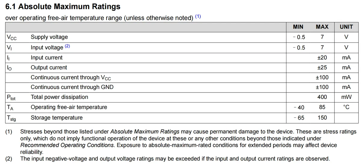
This is the absolute maximum rating table for PCA9546A, the key points are as follows:
- Power Supply and Voltage:
Vcc(supply voltage) andVi(input voltage) both have a range of -0.5 to 7V; - Current Limitations:
Ii(input current) max. ±20 mA,Io(output current) max. ±25 mA,Vcc/GNDcontinuous current max. ±100 mA; - Power Consumption and Temperature:
Ptot(total power consumption) max. 400 mW,TA(operating temperature) ranges from -40℃ to 85℃,Tstg(storage temperature) ranges from -65℃ to 150℃;
NOTE: Exceeding these rated values may damage the device, and these are stress parameters that do not imply the device can operate properly under such conditions; prolonged exposure will affect reliability.
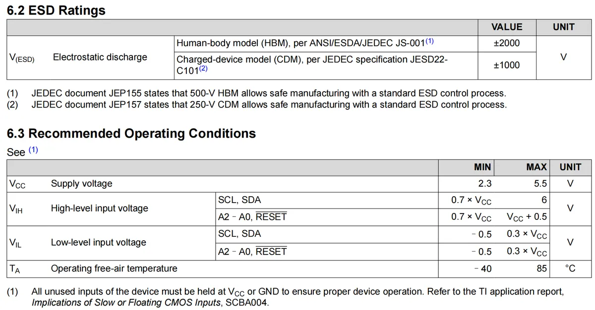
This section contains PCA9546A 's ESD ratings and key points of recommended operating conditions:
ESDRatings: The electrostatic discharge (V (ESD)) tolerance is ±2000V under the Human Body Model (HBM) and ±1000V under the Charged Device Model (CDM), both of which are higher than the safety voltage specified in the standardESDcontrol procedures;- Recommended Operating Conditions: The supply voltage (
Vcc) ranges from 2.3 V to 5.5 V; for high-level input voltage (VIH), theSCL/SDApins range from 0.7×Vccto 6 V, theA2-A0/RESET(reset pin, active low) pins range from 0.7×VcctoVcc+ 0.5 V; for low-level input voltage (VIL), all relevant pins uniformly range from -0.5 V to 0.3×Vcc; the operating temperature (TA) ranges from -40℃ to 85℃, and unused input pins must be connected toVccorGNDto ensure normal operation of the device.

This is the thermal information sheet for PCA9546A, which mainly presents the junction-to-ambient thermal resistance (in ℃/W) corresponding to its various 16-pin packages (DGV, DW, PW, RGV, RGY, D): RθJA. The thermal resistance values vary across different packages; for instance, the DW package has a value of 57, the RGY package has a value of 50, and the DGV package has a value of 120. This parameter represents the thermal transfer resistance between the device junction temperature and the ambient temperature. Different packages correspond to different thermal resistances, which directly affects the heat dissipation performance of the device.
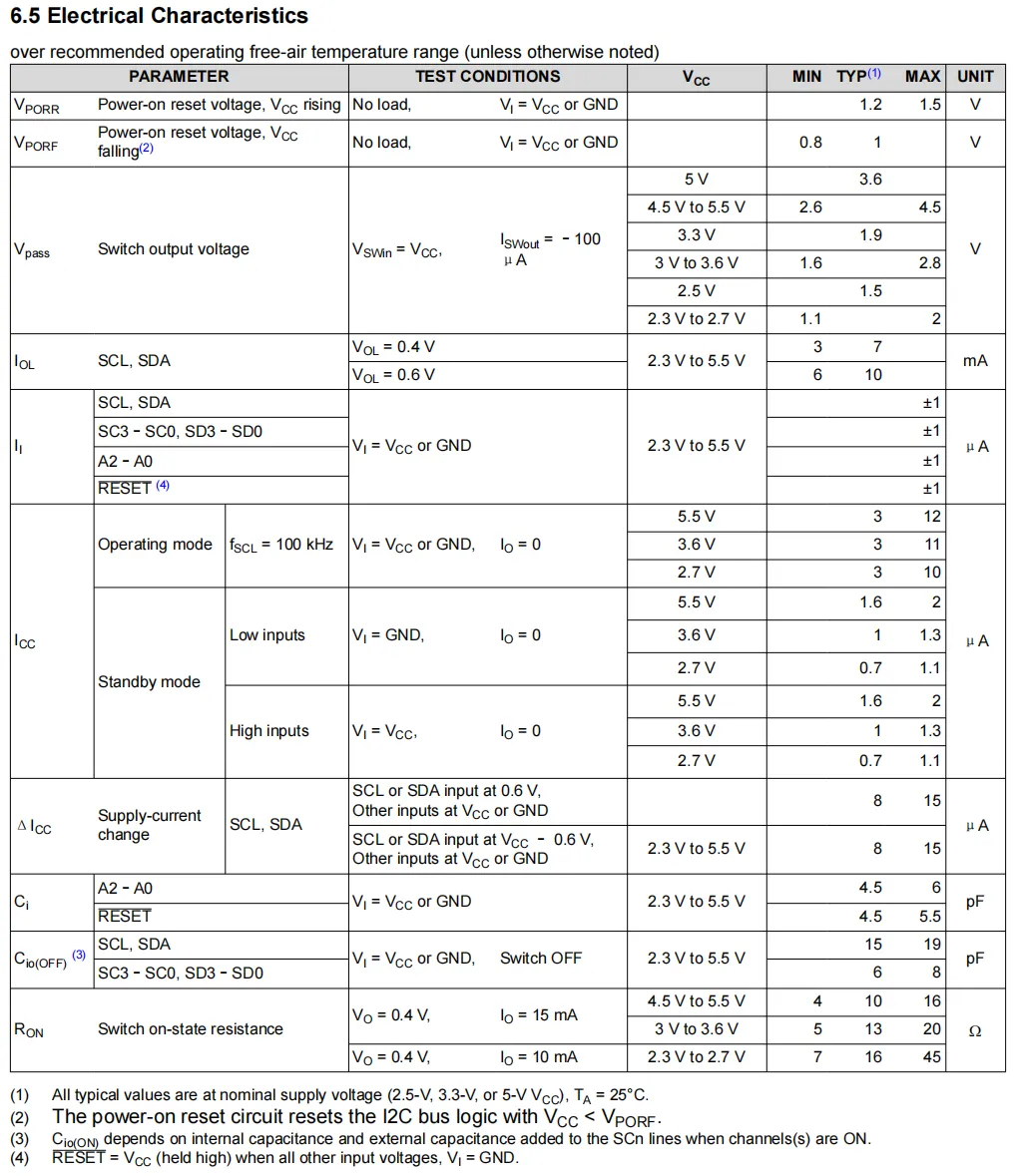
This is the electrical characteristics table for PCA9546A, with the core key points as follows:
- Power-on reset voltage:
VPOCR(whenVccrises): typical 1.2V, maximum 1.5V;VPOCF(whenVccfalls): typical 1V; different thresholds correspond to differentVcclevels, which are used to reset theI2Cbus logic during power-on. - Switching Characteristics:
Vpass(switch output voltage) has a corresponding range that varies with theVccrange and load;RON(switch on-resistance) ranges from 4 to 45Ω under differentVccconditions. - Current parameters:
IOL(SCL/SDAlow-level output current) ranges from 3 to 10 mA;II(input leakage current) has a maximum value of ±1 μA for each pin;ICC(power supply current) is in the microampere range in operating mode, and the current in standby mode is even lower (minimum 0.7 μA), reflecting the low-power characteristic. - Capacitance Parameters:
Ci(input capacitance) is approximately 4.5~6pF;Cx (on)(capacitance when the channel is conducting) on pins such asSCL/SDAis 5~19pF.
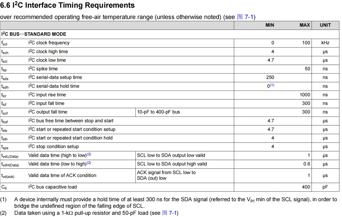
These are the PCA9546A I2C interface timing requirements (Standard Mode), the key points are as follows:
- Clock parameters:
f_scl(I2C clock frequency) max. 100kHz;t_sch(clock high time) min. 4μs,t_scl(clock low time) min. 4.7μs. - Signal Timing:
t_sds(serial data setup time) min. 250 ns;t_sdh(data hold time) nominal 0 ns, but a minimum of 300 ns is actually required internally;t_ir(input rise time) max. 1000 ns;t_if(input fall time) max. 300 ns. - Bus Timing:
t_buf(bus idle time from stop to start) is at least 4.7μs; the setup time and hold time for start/repeated start are at least 4.7μs and 4μs respectively, and the setup time for stop condition is at least 4μs. - Data and load: The valid data time for high-low level switching is 1μs and 0.6μs respectively,
ACKsignal valid time is 1μs;I2Cbus capacitive loadC_bis up to 400pF.
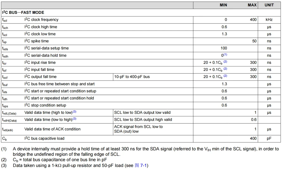
This is the PCA9546A I2C interface fast-mode timing requirements, the key points (more efficient than the standard mode) are as follows:
- Clock parameters:
f_scl(I2C clock frequency) max. 400kHz;t_sch(clock high time) min. 0.6μs,t_scl(clock low time) min. 1.3μs, featuring more compact timing. - Signal Timing:
t_sds(serial data setup time) is at least 100ns;t_icr/t_icf(input rise/fall time) has a minimum value of 20 + 0.1 ×C_b(C_bis the bus capacitance) and a maximum value of 300ns. - Bus Timing:
t_buf(bus idle time between stop and start) is at least 1.3μs; the setup and hold times for start/repeated start, as well as the setup time for stop condition, are all at least 0.6μs, which is shorter than that of the standard mode. - Other: switching between high and low data levels,
ACKsignal valid duration is consistent with that in standard mode,I2Cbus capacitive loadC_bremains a maximum of 400 pF.
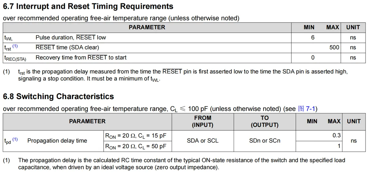
This section covers PCA9546A the key points of reset timing and switching characteristics:
- Interrupt and Reset Timing:
tWL(RESETlow-level pulse duration): min. 6 ns;tRST(RESETtoSDAclear time): max. 500 ns;tREC (STA)(reset-to-startup recovery time): min. 0 ns. - Switching Characteristics:
tPD(SDA/SCLtoSDn/SCnpropagation delay): WithRON= 20Ω, the maximum value is 0.3ns under load capacitanceCL= 15pF, and 1ns underCL= 50pF; this delay is determined by theRCtime constant of the switch on-resistance and load capacitance.
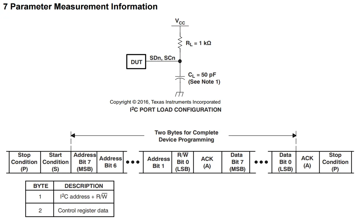
This section contains PCA9546A parameter measurement related information, the key points include:
- I2C Port Load Configuration: During measurement, the
DUThas a 1kΩ pull-up resistor (toVcc) and a 50pF load capacitor connected to itsSDn/SCnpins, which is the standard load condition for parameter testing. - Programming Timing: Device configuration shall be completed via 2-byte
I2Ccommunication, with the procedure being "Stop Condition → Start Condition → 1st Byte (I2CAddress + Read/Write Bit) →ACK→ 2nd Byte (Control Register Data) →ACK→ Stop Condition"; channel selection and other function configurations are implemented via these two bytes.
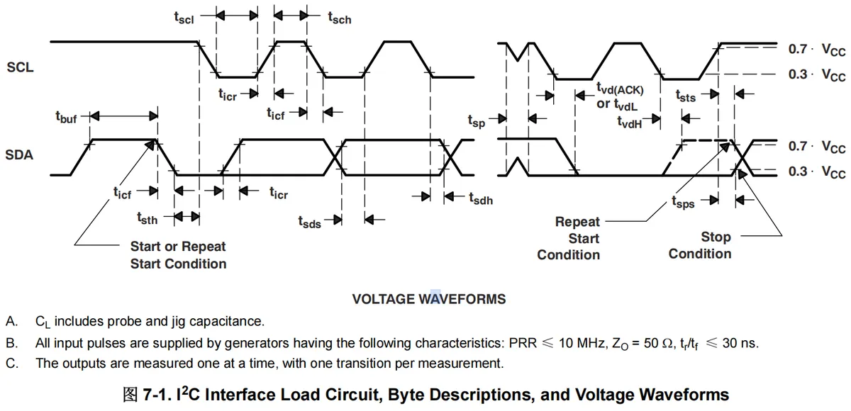
This is the PCA9546A I2C interface voltage waveform diagram, which illustrates the actual timing characteristics of the SCL and SDA signals. The corresponding waveform positions are marked in the diagram for parameters including clock high/low time (t_scl / t_sch), bus idle time (t_buf), timing parameters related to start/repeated start/stop conditions (t_sth / t_sts / t_sps), and data setup/hold time (t_sds / t_sdh);The notes below supplement that the load capacitance includes the capacitance of the probe and the fixture, the characteristics of the generator for the input pulse, and the output adopts the mode of "single measurement for a single transition".
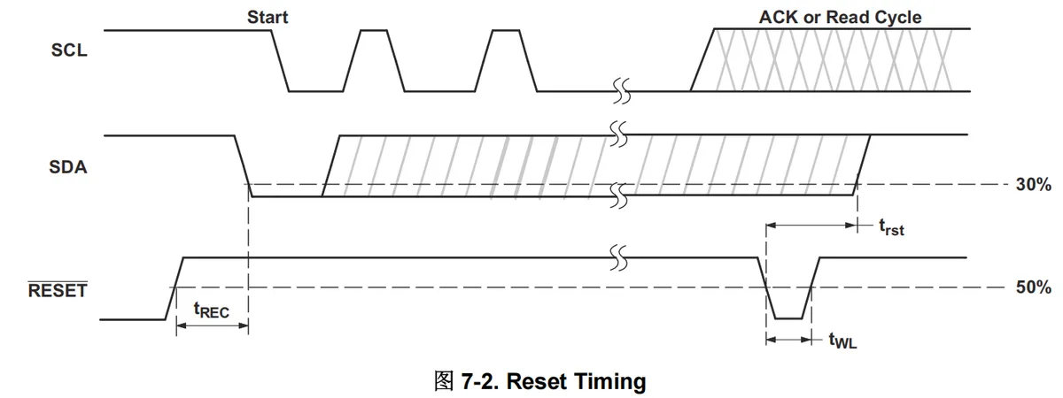
This is the reset timing waveform diagram of PCA9546A , showing the timing coordination of SCL , SDA and RESET signals: the figure wins the bidding for the RESET signal's tREC (recovery time from reset to start), tWL (low-level pulse duration), and tRST (delay time from RESET to SDA returning to high level); at the same time, it is associated with the signal stage of start conditions and ACK /read cycles, clearly showing the timing interaction of each signal during the reset process.
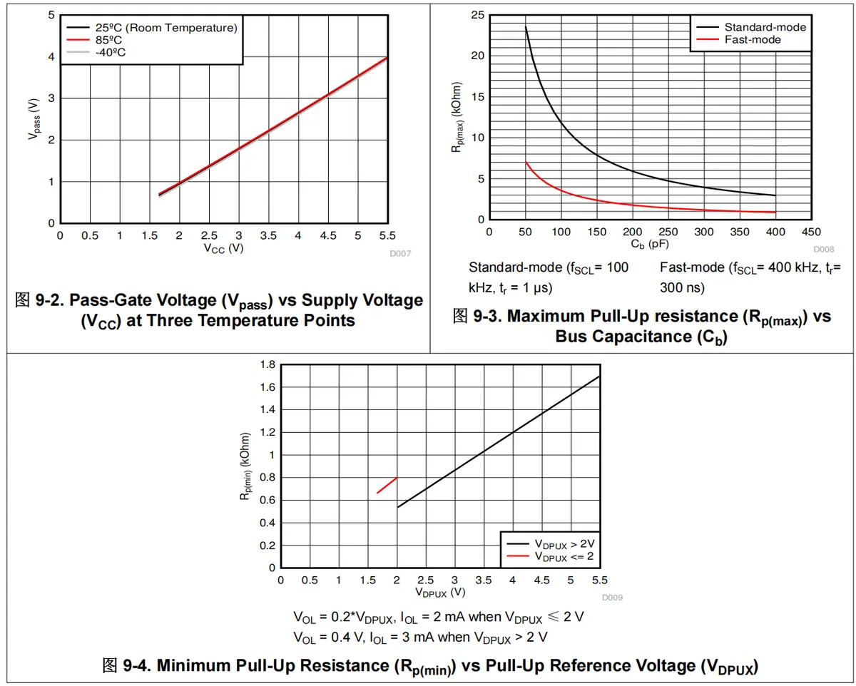
These three graphs are PCA9546A design reference curves:
- Figure 9.2 illustrates the relationship that the transmission gate voltage (
Vpass) increases as the supply voltage (Vcc) rises at different temperatures; - Figure 9.3 illustrates the trend that the maximum pull-up resistor (
Rp (max)modes, and the maximum pull-up resistor for the fast mode is smaller;Cb) increases in the standard/fastI2Cmodes, and the maximum pull-up resistor for the fast mode is smaller; - Figure 9.4 illustrates the variation of the minimum pull-up resistance (
VDPUX) corresponding to different pull-up reference voltages. The higher the pull-up voltage, the larger the minimum pull-up resistance. Additionally, there are differences in the curve characteristics between the cases whereRp (min)) and those whereVDPUX≤2V and >2V. These curves are used to assist in matching the power supply, pull-up resistance, and bus parameters during design.
2.5 Reference Circuit
2.5.1 Reference Circuit
In the following figure, the I2C master device connects to the SDA / SCL / RESET pins of the chip. Each of the 4 channels is connected to an independent pull-up resistor, and the chip address is configured via the A0/A1/A2 pins, so as to realize orderly communication management of multiple slave devices.
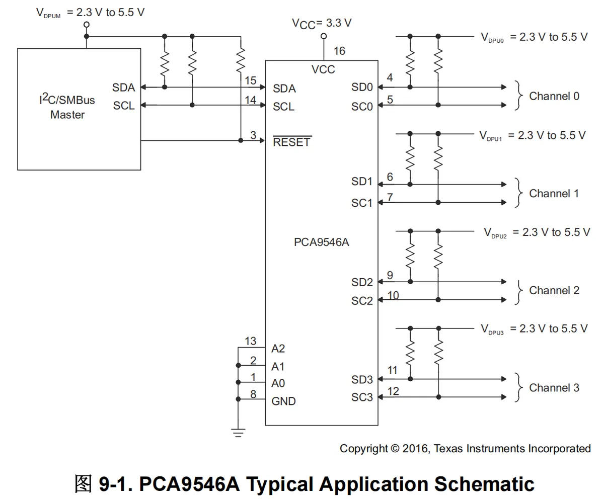
PCA9546A is a 4-channel I2C switch, which is primarily used to resolve address conflicts of I2C slave devices (for example, 4 temperature sensors with the same address are connected to 4 channels respectively, and the corresponding channel is enabled as needed to read data), and can also distribute bus capacitance (connect non-conflicting slave devices to multiple channels to reduce the load of a single channel).
It supports voltage conversion: pull-up resistors of different voltages can be connected to the master device and each channel; if the voltages are consistent, the turn-on voltage of the switch will be the same as the pull-up voltage, which facilitates adaptation to devices with different voltages.
2.5.2 Power Supply Requirements
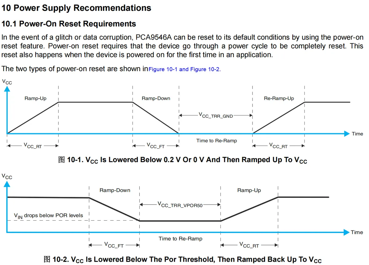
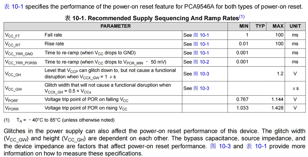
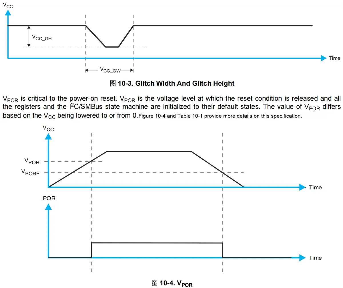
PCA9546A has two power-on reset modes:
- Bring
Vccdown to 0.2V (or 0V) and then raise it back; - Bring
Vccbelow the POR threshold and then raise it back up.
The above figure presents timing parameters such as the power supply falling/rise rate and power-on reset waiting time, as well as the voltage transition point of POR when Vcc rises/falls; it also indicates that power supply glitches will affect reset performance, so the width and height of glitches need to be controlled.
2.6 Chip Configuration
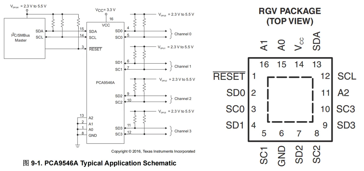
We can configure the chip address by configuring A0 to A2 to connect to GND / VCC.
2.7 Communication Interfaces and Related Protocols
2.7.1 Brief Introduction
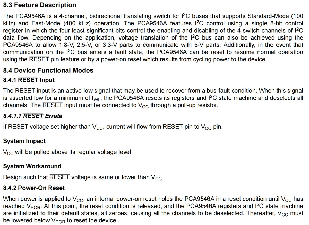
PCA9546A is a 4-channel I2C bidirectional switch, whose core functions are based on the basic features of the I2C bus:
- Supports
I2Cstandard mode (100kHz) and fast mode (400kHz) - Channel control is implemented via an 8-bit control register — the lower 4 bits of the register correspond to the "on/off" status of the 4 channels (bit-wise control logic is commonly used in embedded systems, where 1 bit corresponds to the enable/disable state of one function);
- Voltage conversion capability: By leveraging
I2Cthe "open-drain output" feature (the logic level of an open-drain bus is determined by the external pull-up resistor), connecting pull-up resistors of different voltages to separate channels enables communication between 1.8V/2.5V/3.3V devices and 5V devices; - Fault recovery: When the
I2Cbus is stuck, it can be recovered via reset, which meets the basic operation and maintenance requirements for bus fault handling.
RESET reset pin is an active-low pin. When the pin is held at a low level for at least tWL (6ns in the previous table), the chip will reset the registers, I2C finite-state machine, and turn off all channels (restore the initial state of the bus):
- The pin must be connected to a pull-up resistor to
Vcc(active-low pins are supposed to be kept at high level to remain "inactive" by default, and the pull-up resistor prevents false triggering caused by floating pins); - If the
RESETvoltage is higher thanVcc, a sink current phenomenon described as "current flows fromRESETtoVcc" will occur, which violates the basic rule of power domain level matching. It is necessary to ensure that theRESETvoltage does not exceedVcc.
Note at power-on reset:
- Upon power-up, the internal
POR(Power-On Reset) circuit keeps the chip in a "reset state" untilVccreaches the "power-on reset voltage"(VPOCRin the preceding table); - When
Vccmeets the required specification,PORreleases the reset, and the registers and finite-state machine are initialized to "all zeros"(corresponding to all channels being turned off); - To perform a power-on reset again, you need to
Vccpull it below the "power-on reset voltage", then power on the device again (to ensure the chip starts from the "initial state" and avoid instability during power-up).
2.7.2 Fundamentals of I2C Communication
We read from and write to I2C PCA9546A via its control register:
- The write timing sequence is "Start → Slave address (the first 5 bits are fixed as
1110, the last 3 bits areA2/A1/A0, and the read/write bit is 0) →ACK→ Control register data (the lower 4 bitsB3-B0correspond to the on/off status of the 4 channels) →ACK→ Stop"; - The read timing is similar (when the read/write bit is 1), and finally the master sends
NACKbefore stopping, so as to configure the channel status.
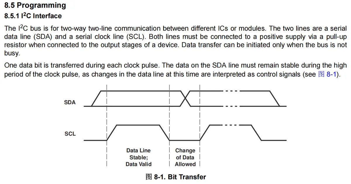
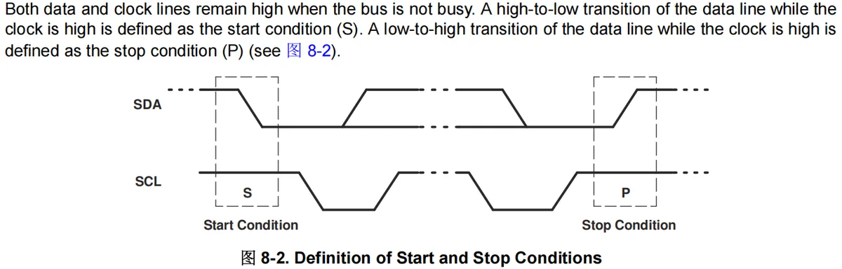
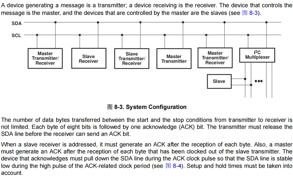
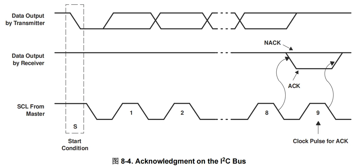
I2C is a two-wire (SDA / SCL, requiring pull-up resistors) bidirectional communication protocol. When the bus is idle, both lines are at a high level; during bit transmission, SDA must remain stable while SCL is at a high level. The falling/rising edge of SDA when SCL is high corresponds to the start (S) and stop (P) conditions respectively. The master device controls the bus, while the slave device responds. After every 8 bits of data, the receiver must send an ACK (pulling SDA low) for acknowledgment.
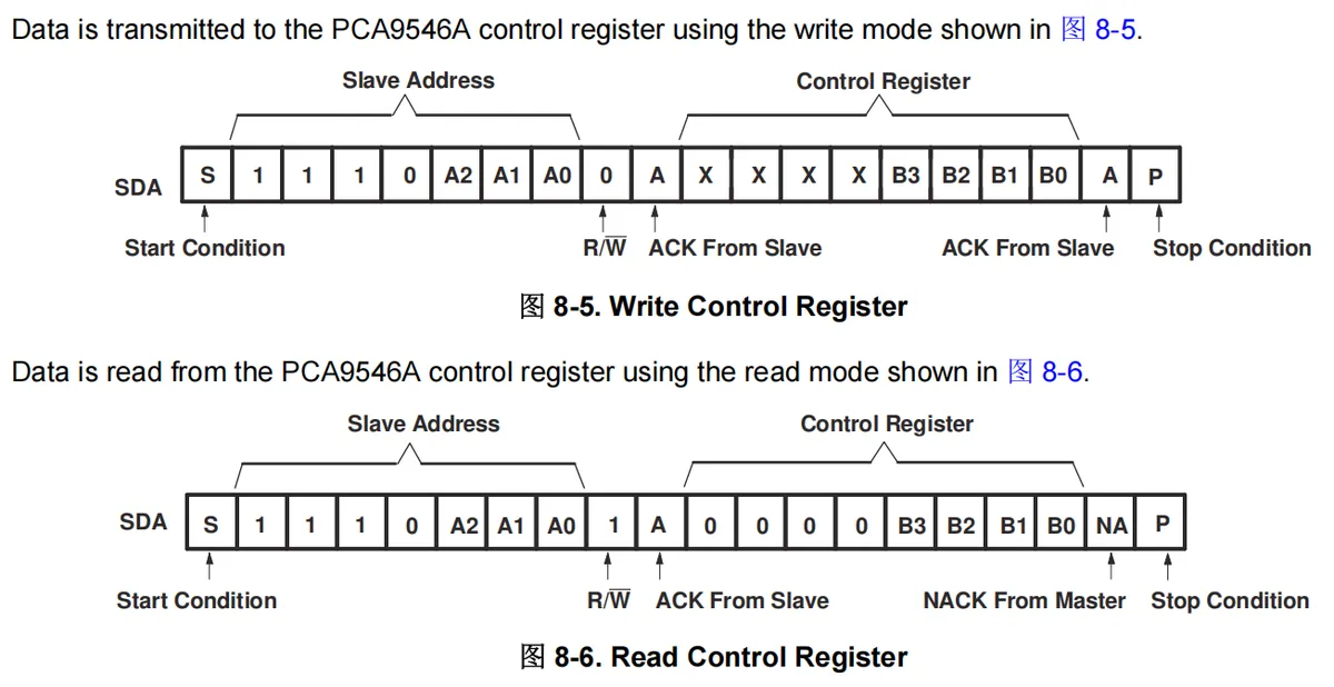
2.7.3 Related Control Registers
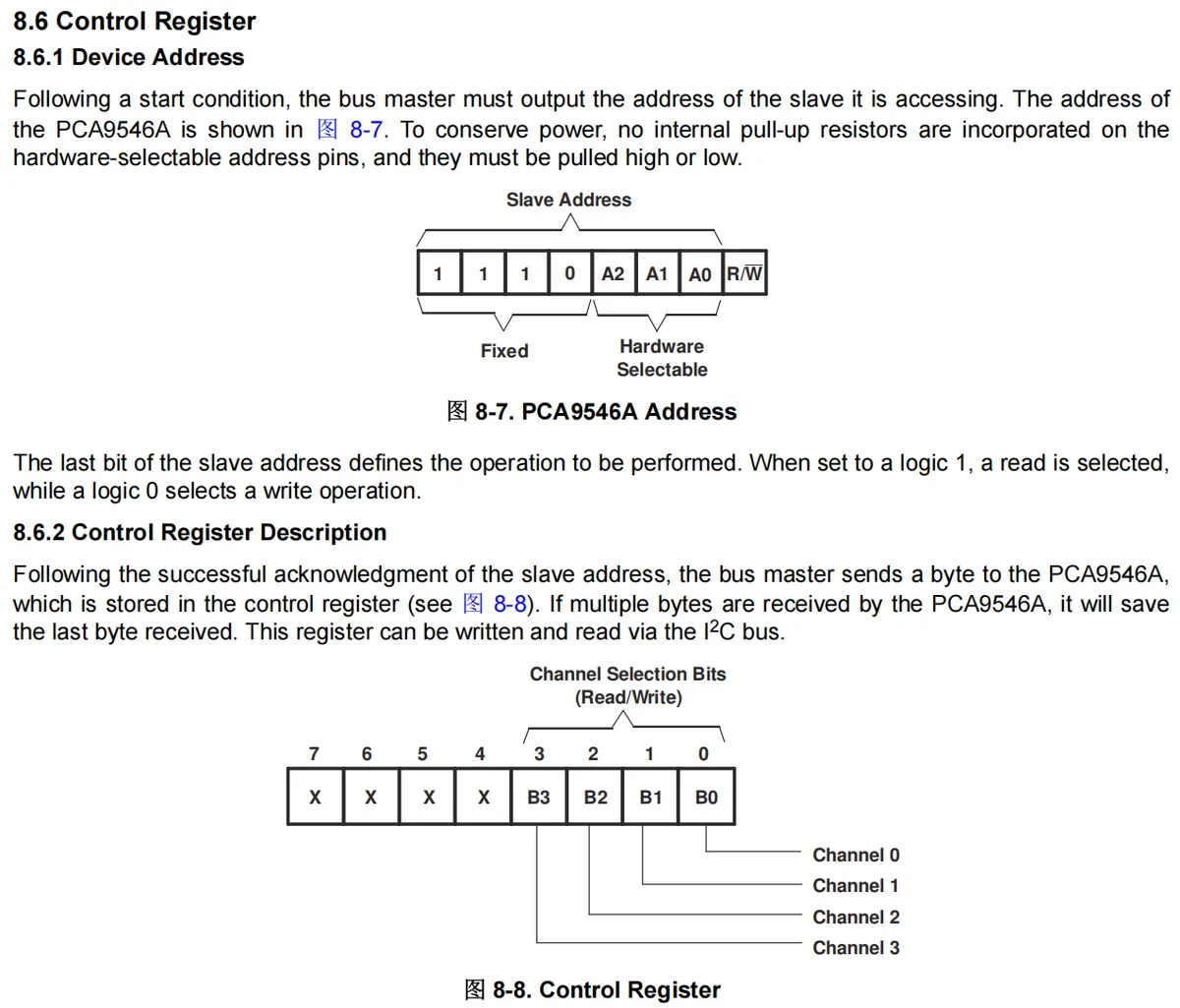

PCA9546A Device Address and Control Register Rules:
- Device Address: The first 5 bits of the address are fixed as
1110, the last 3 bits are configured viaA2/A1/A0hardware pins (external pull-up/pull-down required, no internal pull-up), and the last 1 bit is the read/write bit (1for read,0for write), which is used to specify the operation type for the chip. - Control Register: It is an 8-bit register, the upper 4 bits (
B7–B4) are reserved (denoted asX), and the lower 4 bits (B3–B0) serve as selection bits for the 4 channels —B3corresponds to Channel 3,B2corresponds to Channel 2,B1corresponds to Channel 1,B0corresponds to Channel 0; a bit value of1enables the corresponding channel, and a value of0disables it. Multiple channels can be enabled simultaneously (e. g.,B2= 1, B1= 1enables Channel 1 and Channel 2). - Effective Rule: The control register must be written after the device address is acknowledged by
ACK, and the channel configuration will not take effect until the stop condition of theI2Cbus occurs (to ensure that the bus is at high level when the channel is activated and avoid false triggering); after power-on / reset, all registers default to0, and all channels are disabled.
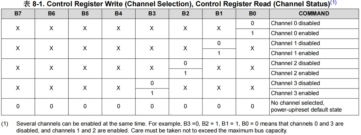
2.8 PCB Routing Precautions
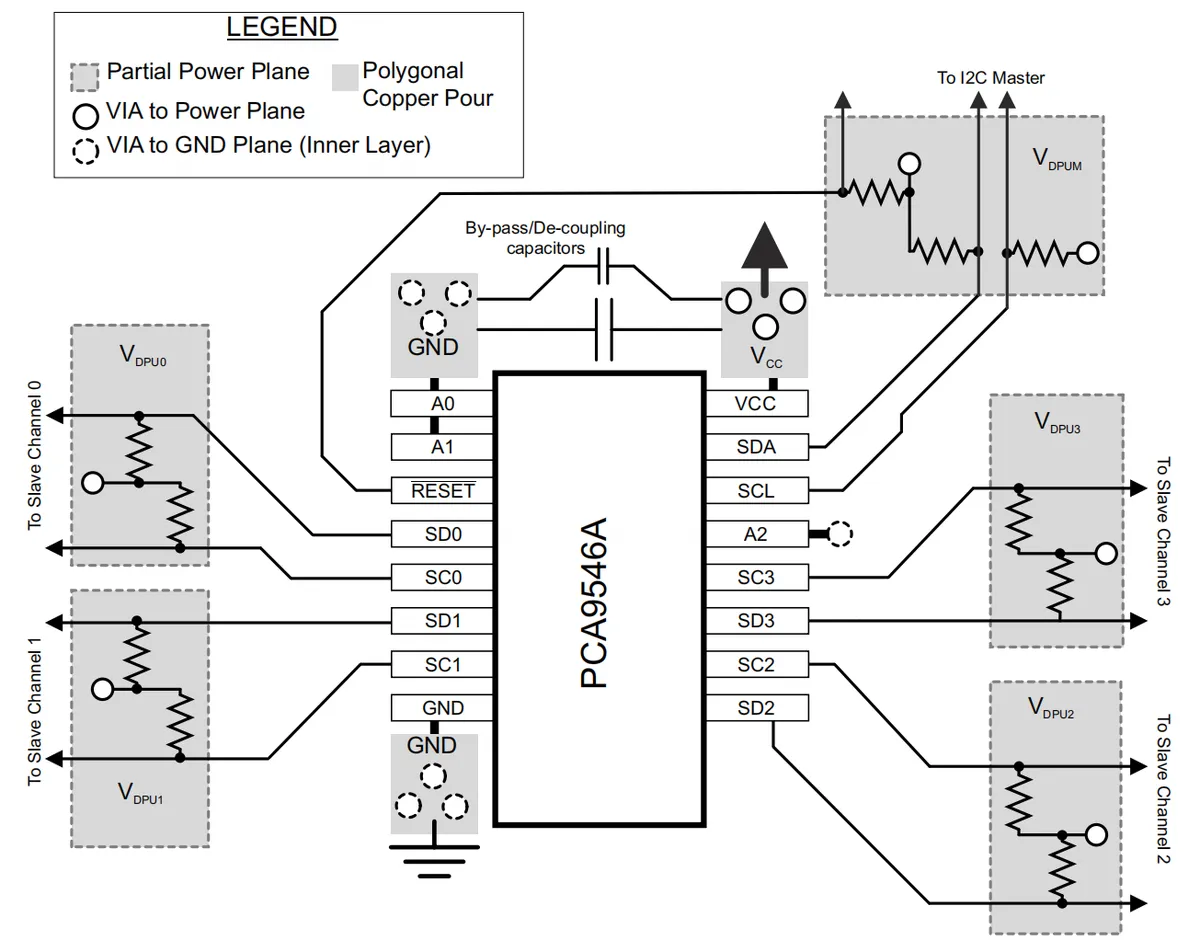
PCA9546A PCB layout precautions are as follows:
- No high-speed design considerations required: Since
I2Csignal rate is not high, there is no need for high-speed routing requirements such as impedance matching and differential pairs; - Grounding Design: It is recommended to arrange a dedicated ground plane on the inner layer, and the grounding pins shall be connected to the ground plane through wide copper pouring and multiple vias to ensure a low-impedance grounding path;
- Power Supply Decoupling:
Vccpins shall be connected to decoupling capacitors (large capacitors suppress power supply glitches, small capacitors filter high-frequency ripples) to stabilize the power supply voltage; - Voltage Plane Processing:
- When no voltage conversion is required, all pull-up voltages (
VDPUX) andVcccan be at the same potential, and a single copper plane can be used to connect all pull-up resistors; - When voltage conversion is required, different
VDPUXshall be isolated by split planes to avoid voltage crosstalk;
- When no voltage conversion is required, all pull-up voltages (
- Reduce bus capacitance:
SCn/SDndata lines shall be as short as possible, and the trace width shall be as small as possible (e. g., 5-10mil, adjusted according to copper thickness) to reduce the parasitic capacitance ofPCB.
III. Instructions for Circuit Engineering and Module Usage
3.1 Circuit Source Engineering
To obtain the source code of the circuit, please follow the official account [Freak Embedded]
3.2 Module Usage Instructions
The schematic diagram of this module is as follows:
SCH_4-Channel I2C Multiplexer Expansion Module Based on PCA9546ADR_v1.0_2025-11-26.pdf 2.3 MB
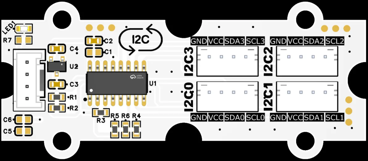
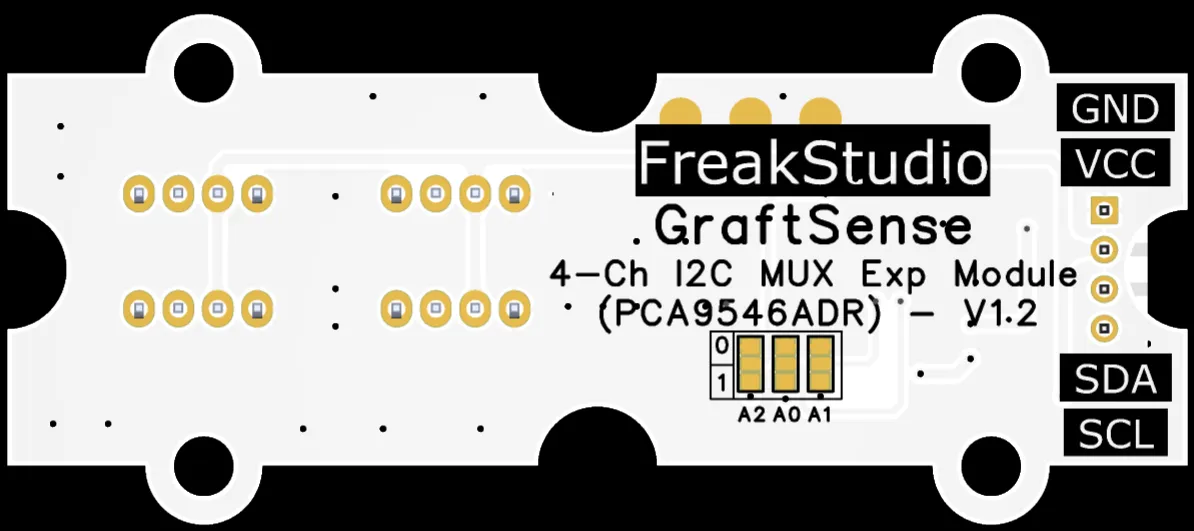
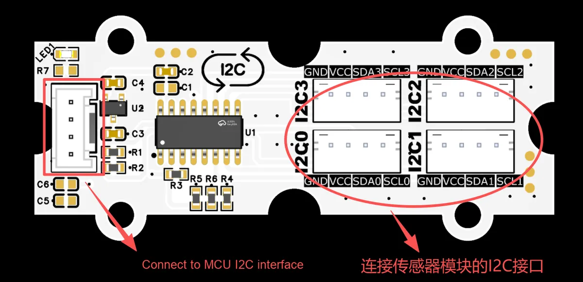
This module provides an I2C interface: simply connect the I2C interface of the MCU to the 4P communication interface on the left side of the module; then connect the I2C interfaces of other sensor modules to the four I2C interfaces on the right side of the module to complete the connection.
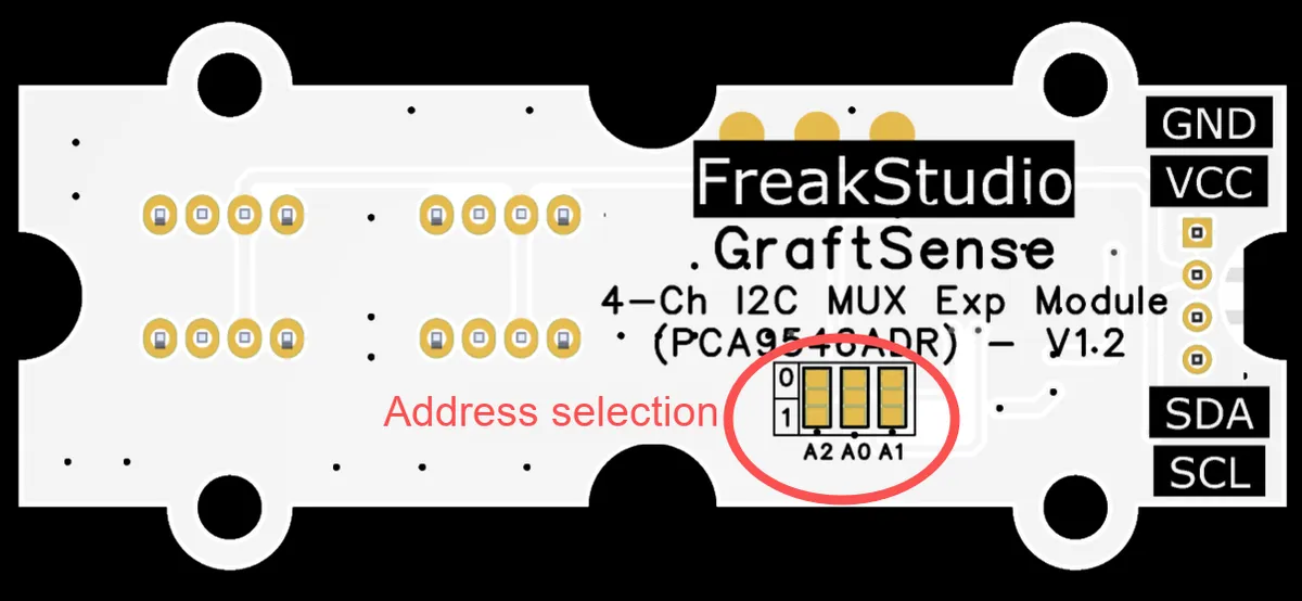
In addition to the basic interface connection operation, we can also complete the setting of the module's I2C address by soldering the short-circuit points on the back of the module — these short-circuit points correspond to the A2, A0, and A1 pins respectively, and different addresses can be configured by soldering as needed.
3.3 Application Experiment
Here, we use the GraftPort-RP2040 development board for testing, and we will mount a 4-channel I2C multiplexer expansion module with the PCA9546ADR chip to establish a communication connection with the main control unit via the I2C interface. Meanwhile, two types of functional modules are additionally connected to this expansion module:
- RTC real-time clock module based on DS1307 chip is connected to
the I2C0 port of the 4-channel I2C multiplexer expansion module based on PCA9546ADR - 0.96-inch SSD1306-OLED module is connected to the I2C1 port of the 4-channel I2C multiplexer expansion module based on PCA9546ADR
I2C1
Here, we first use the HY2.0-4P cable to connect the module to the GraftPort-RP2040 development board's I2C1 interface:
The module connections are shown in the following table:
Development Board Pins | Module Pins | Description |
Pin 2 |
|
|
Pin 3 |
|
|
- |
| Here we use the RTC real-time clock module based on the DS1307 chip with an address of |
- |
| Here we use the 0.96-inch SSD1306-OLED module with the address of |
Here, we need to search for relevant driver packages on uPyPI: https://upypi.net/zh/
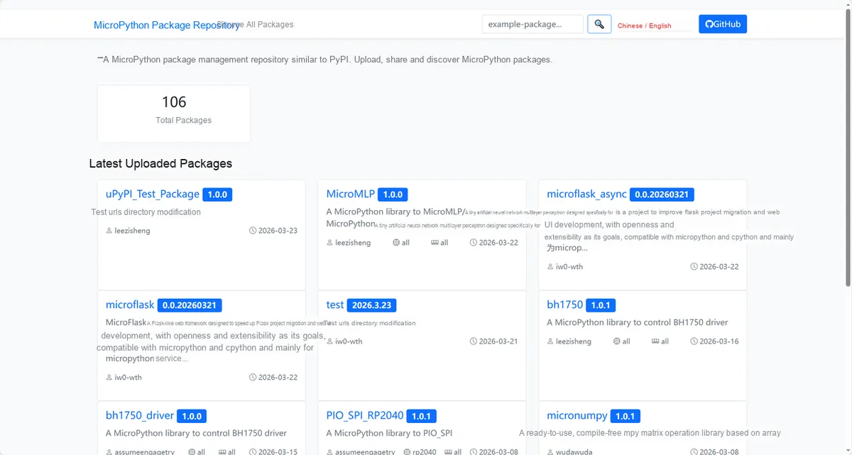
Enter pca9546_driver to search, and the following will be displayed:

Click to copy the local installation command:
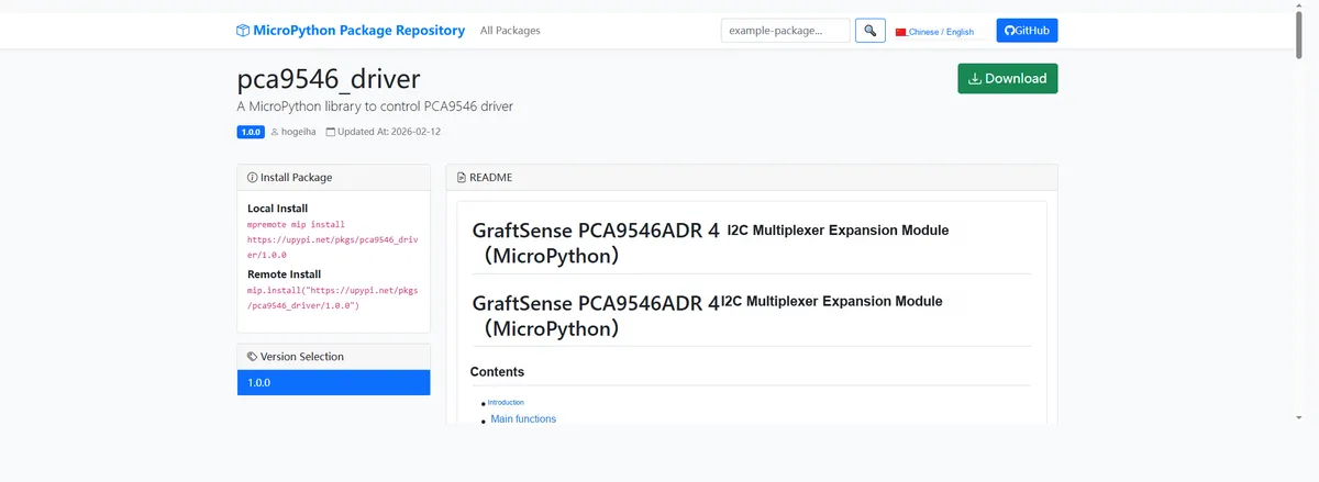
Here, we can use the mip tool to import module driver library code. Below are the usage commands for the mpremote tool:
mpremote mip install github:FreakStudioCN/GraftSense-Drivers-MicroPython/misc/pca9546_driverImport the 4-channel I2C multiplexer expansion module based on PCA9546ADR - MicroPython driver code, then copy the following main.py code into our project:
# Python env   : MicroPython v1.23.0
# -*- coding: utf-8 -*-
# @Time    : 2025/09/08 15:00
# @Author  : 侯钧瀚
# @File    : mian.py
# @Description : Example program of I2C multiplexing based on the PCA9546ADR 4-channel multiplexer
# ======================================== Import Modules =========================================
# Import MicroPython standard library modules
from machine import Pin, I2C
# Import the time module
import time

from pca9546adr import PCA9546ADR
# ======================================== Global Variables ============================================

# ======================================== Functions ============================================

# ======================================== Custom Classes ============================================

# ======================================== Initialization ==========================================
# Power-on delay of 3 s
time.sleep(3)
# Print debug message
print("FreakStudio: Testing PCA9546ADR4 I2C Multiplexer Modules")

# Initialize I2C bus
i2c = I2C(1, scl=Pin(2), sda=Pin(3))

pca = PCA9546ADR(i2c)


# ========================================  Main Program  ===========================================

while True:

    pca.disable_all()
    pca.select_channel(0)
    print("0 address",i2c.scan())

    time.sleep(4)

    pca.disable_all()
    pca.select_channel(1)
    print("1 address",i2c.scan())
To flash the code, open a terminal and use the mpremote tool to connect to the main controller; the output is as follows:
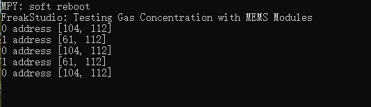
It can be seen that we are able to scan out the correct address on the specified channel;
4-channel I2C multiplexer expansion module based on PCA9546ADR has the address of 112, which is 0x70
0.96-inch SSD1306-OLED module, with the address being 61, i. e. 0x3D
RTC real-time clock module based on the DS1307 chip, with the address being 104, which is 0x68
IV. Drivers
pca9546_driver.zip 4 KB
5. BOM & Recommended Alternative Parts
None.
VI. Revision History
Document Version | Date of Revision | Modifier | Revised Content |
v1.0 | 2025-11-26 | Li Zisheng | Initialize the document The BOM sheet has not been finally checked, the driver has not been re-verified, and the 3.3 application experiment Not yet specified. |
v1.1 | 2025-12-29 | Li Zisheng | Added application experiments and production files |
v1.2 | 2025-12-31 | Xin Ruili | Create an open version of the document based on the internal document version v1.1. |
v1.3 | 2026-03-29 | Xin Ruili | Modified the application experiment section |
VII. Relevant Materials
7.1 Chip Datasheet
pca9546a.pdf 2.8 MB
7.2 Unique Icons for PCB Silk Screen