Contents
- I. Module Introduction
- II. Introduction to Main Chips
- 2.1 Chip Overview
- 2.2 Pin Definition
- 2.3 Functional Block Diagram
- 2.4 Performance Parameters
- 2.5 Reference Circuit
- 2.6 Chip Configuration
- 2.7 Communication Interfaces and Related Protocols
- 2.8 PCB Routing Notes
- III. Circuit Engineering
- 3.1 Circuit Source Engineering
- 3.2 Module Usage Instructions
- 3.3 Application Experiment
- IV. Drivers
- 5. BOM & Recommended Alternative Parts
- 6. Revision History
- VII. Relevant Materials
- 7.1 Chip Datasheet
- 7.2 Unique Icons for PCB Silk Screen
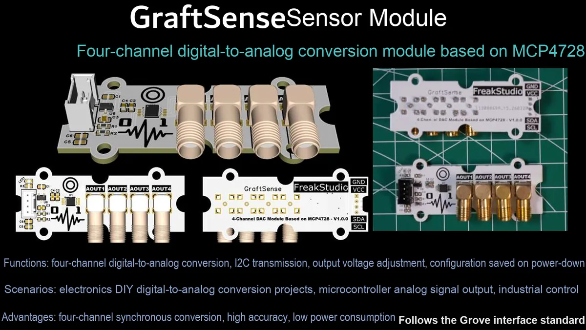
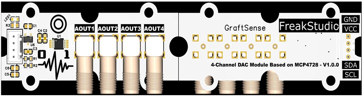
I. Module Introduction
4-channel DAC module based on MCP4728, which adopts the Microchip MCP4728 12-bit 4-channel voltage-output DAC chip solution, has a built-in non-volatile EEPROM and reference voltage source, supports I²C interface communication, and operates with a supply voltage of 2.7V~5.5V;Equipped with a 5V to 3.3V LDO voltage regulator circuit and power filter circuit, it is compatible with 3.3V level, features 12-bit resolution corresponding to 4096-level output, built-in programmable gain amplifier and reference voltage selection (2.048V/4.096V or external VDD). With four-channel independent output capable of controlling four analog signals simultaneously, it is suitable for scenarios such as multi-channel analog control, industrial automation and precision instruments, providing the system with efficient and stable digital-to-analog signal conversion capability.
II. Introduction to Main Chips
MCP4728 is a Microchip -launched 12-bit quad-channel voltage-output DAC chip with built-in non-volatile EEPROM and voltage reference, supporting I²C interface communication, with a resolution of 4096 levels, operating on a 2.7V~5.5V power supply, capable of simultaneously outputting four independent analog voltages, and suitable for multi-channel analog control scenarios.
2.1 Chip Overview
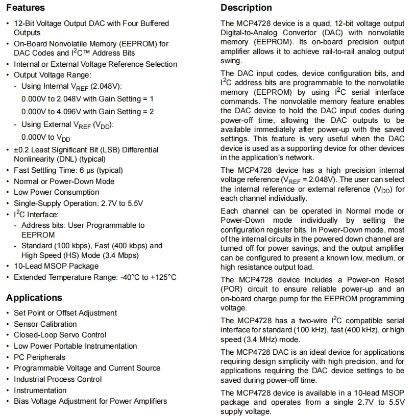
MCP4728 is a 12-bit four-channel voltage-output DAC with built-in non-volatile EEPROM and precision voltage reference, supporting I²C interface (up to 3.4Mbps). It can select internal reference (2.048V/4.096V) or external VDD as the reference, features a resolution of 4096 levels, and has low power consumption and power-off retention functions, making it suitable for multi-channel analog control, precision instruments and other scenarios.
2.2 Pin Definition
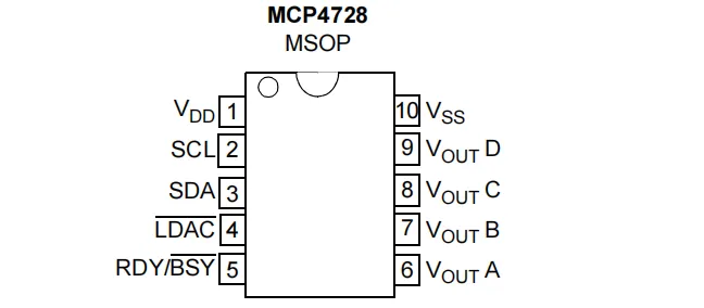
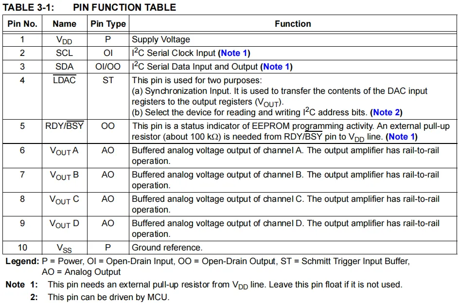
MCP4728 is available in a 10-pin MSOP package with the following pin definitions: Pin 1 VDD (power supply), Pin 2 SCL (I²C clock), Pin 3 SDA (I²C data), Pin 4 LDAC (simultaneous update / address configuration), Pin 5 RDY/BSY (EEPROM programming status), Pins 6~9 VOUTA~VOUTD (four independent analog outputs), and Pin 10 VSS (ground). It features a compact form factor that facilitates high-density PCB layout for multi-channel analog systems.
2.3 Functional Block Diagram
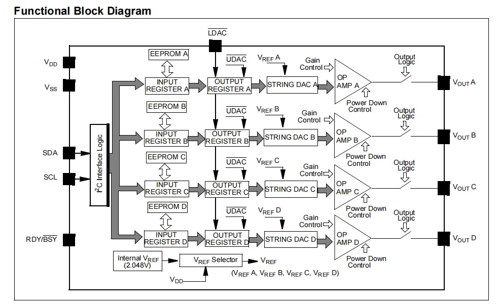
MCP4728 is an integrated four-channel 12-bit voltage output DAC chip that incorporates four independent DAC channels; each channel consists of an input register, an output register, and a serial DAC core, with a built-in 2.048V reference voltage source and non-volatile EEPROM, which can receive digital commands via the I²C interface to write data into the input register;All-channel output registers can be updated synchronously via the LDAC pin. It features flexibly adjustable reference voltage selection and gain configuration, rail-to-rail output capability for the output amplifier, and independent power-down mode control, delivering stable and efficient digital-to-analog signal conversion performance for multi-channel analog control scenarios.
2.4 Performance Parameters
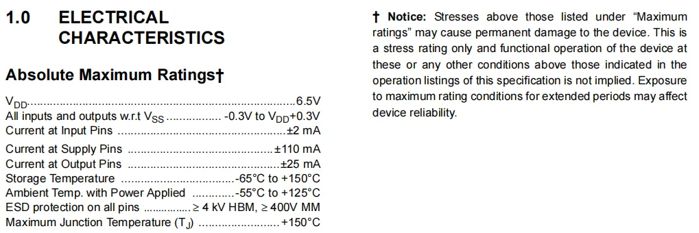
MCP4728 's absolute maximum ratings specify the upper limit of power supply voltage as 6.5V, the voltage range of input/output pins as -0.3V to VDD + 0.3V, as well as limit parameters including pin current, ESD protection (≥4kV HBM) and operating/storage temperature range (-65℃ to 150℃), which provides a safety boundary basis for the reliable use of the chip and circuit protection design.
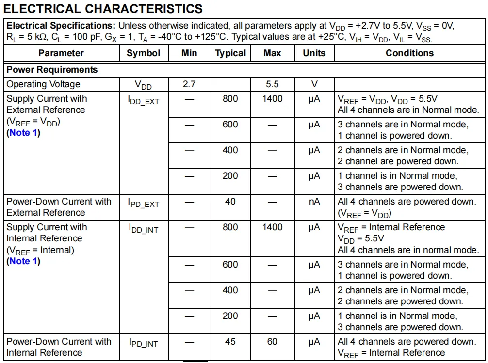
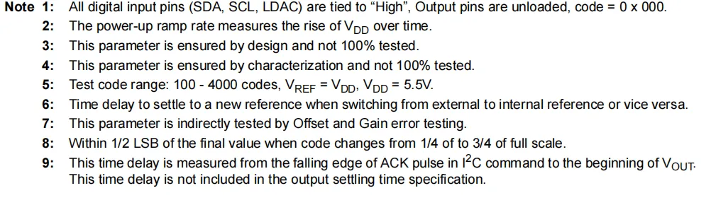
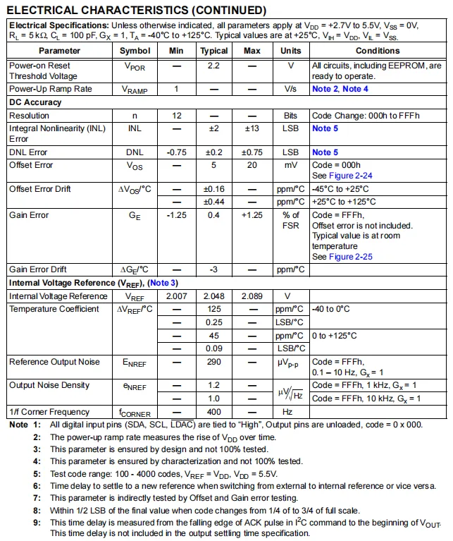
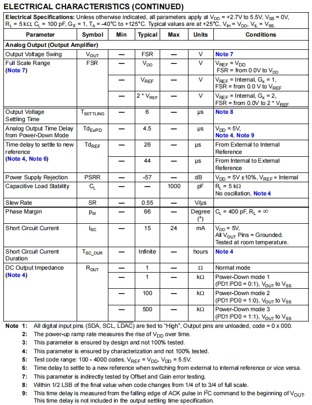
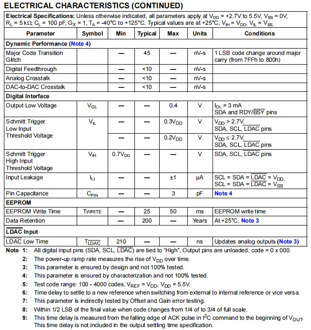
MCP4728 features excellent electrical performance: it operates on a supply voltage of 2.7V to 5.5V, offers 12-bit resolution, has a typical integral non-linearity (INL) value of ±2 LSB, integrates a built-in 2.048V reference voltage, supports rail-to-rail output swing, features a settling time of only 6μs, delivers low-power characteristics (standby current of 0.1μA), has an I²C interface compatible with 3.3V logic levels, and also supports power-off retention as well as multi-channel low crosstalk, making it ideal for high-precision multi-channel analog control applications.
2.5 Reference Circuit
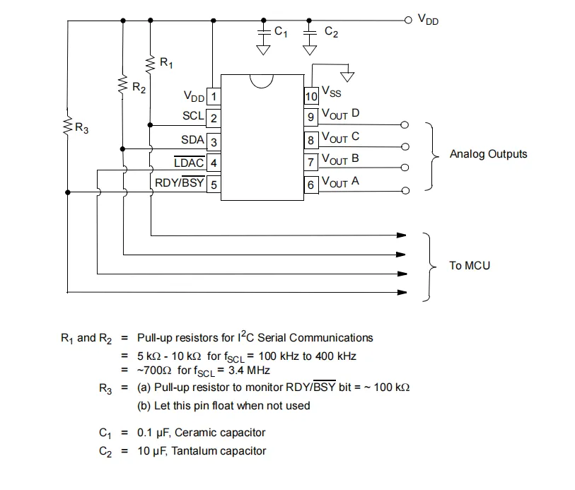
MCP4728 features a typical application circuit that uses the I²C interface; the SDA / SCL pins are externally connected with pull-up resistors of 5kΩ~10kΩ(approx. 700Ω for high-speed mode), a 0.1μF ceramic capacitor and a 10μF tantalum capacitor are connected in parallel at the power supply terminal for filtering, the RDY / BSY pin can be connected to a 100kΩ pull-up resistor to monitor the EEPROM status, it supports four-channel independent analog voltage output, can be directly connected to a 3.3V MCU to realize multi-channel high-precision analog control.
2.6 Chip Configuration
None.
2.7 Communication Interfaces and Related Protocols
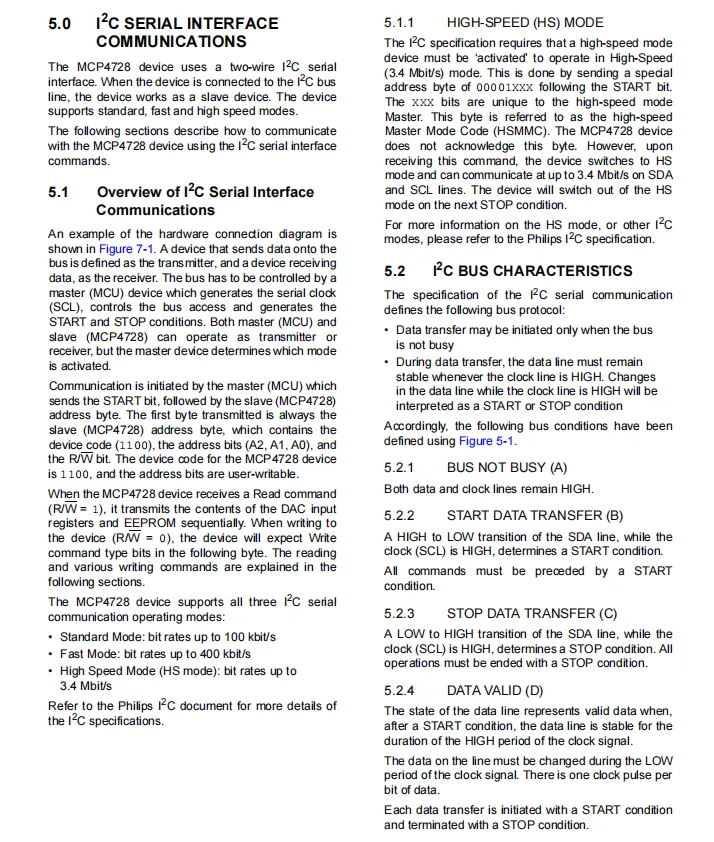
MCP4728 communicates via the I²C serial interface; as a slave device, it supports standard (100kbps), fast (400kbps) and high-speed (3.4Mbps) modes, with a device address consisting of 1101 plus three programmable address bits. Compliant with the I²C bus protocol specifications (including START / STOP conditions, data setup/hold timings, etc.), it enables efficient digital command and data interaction with MCUs, making it suitable for multi-device bus scenarios.
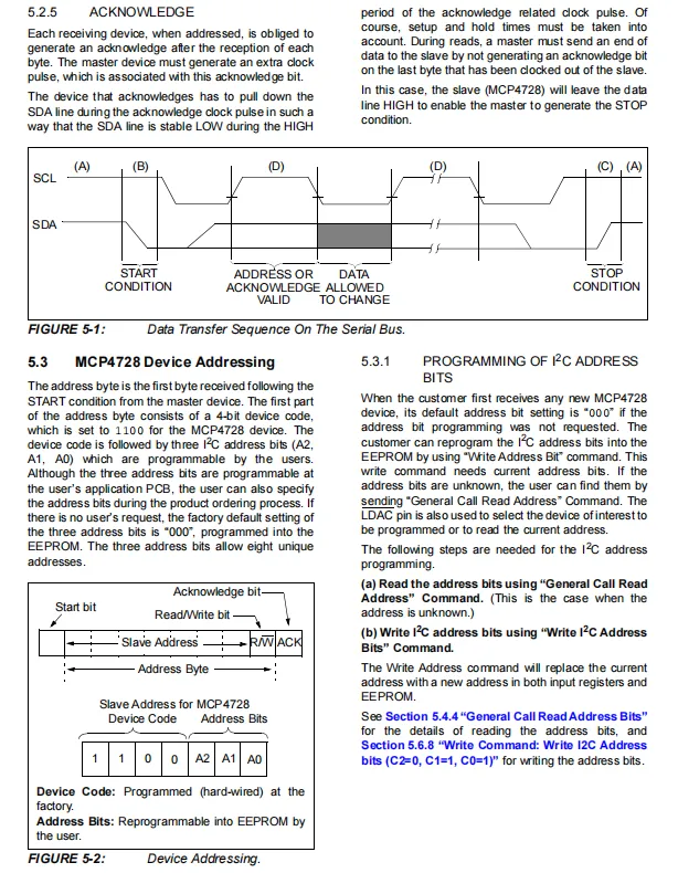
MCP4728 complies with the I²C acknowledgment mechanism: it pulls down the SDA line to generate an acknowledgment pulse after receiving each byte. Its device address consists of a fixed 1101 device code plus three programmable address bits (which can be stored in EEPROM). It supports reading unknown addresses via the general call command, providing flexible and reliable addressing and communication assurance for multi-device I²C bus systems.
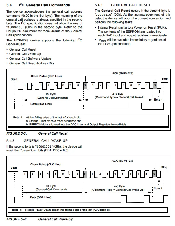
MCP4728 supports I²C general call commands: the chip can be reset via the 0x00 address plus the 0x06 command (equivalent to a power-on reset that loads EEPROM data), or the 0x09 command can be used to wake up powered-down channels, providing efficient batch reset and wakeup capabilities for multi-device bus systems.
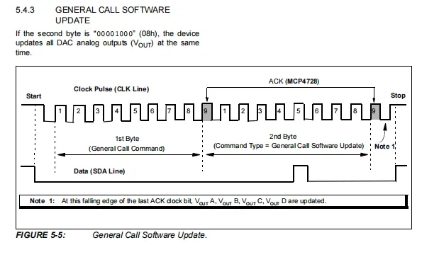
MCP4728 supports the I²C general call software update command: by sending the command 0x00 to the general call address 0x08, the analog outputs of all DAC channels can be updated synchronously, which realizes the synchronous update of multi-channel output and is suitable for control scenarios requiring simultaneous changes of multi-channel analog signals.
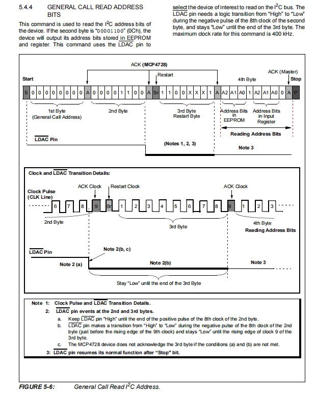
The MCP4728 supports the I²C address, and coordinating with the level transition of the 0x0C command to the 0x00 address, and coordinating with the level transition of the LDAC pin, the I²C address bits stored in the chip's EEPROM can be read, which solves the addressing problem of unknown addresses in a multi-device bus and facilitates system debugging and maintenance.
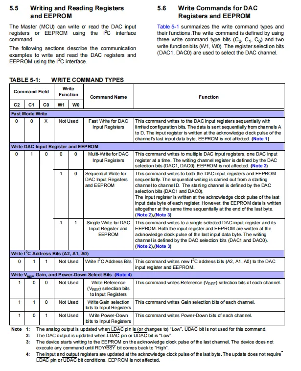
MCP4728 provides a rich set of I²C write commands, supporting fast write, multi-channel / single-channel register plus EEPROM write, address bit programming, as well as reference / gain / power-down mode configuration. It can flexibly realize multi-channel DAC output control and parameter storage, delivering efficient instruction interaction capabilities for high-precision multi-channel analog systems.
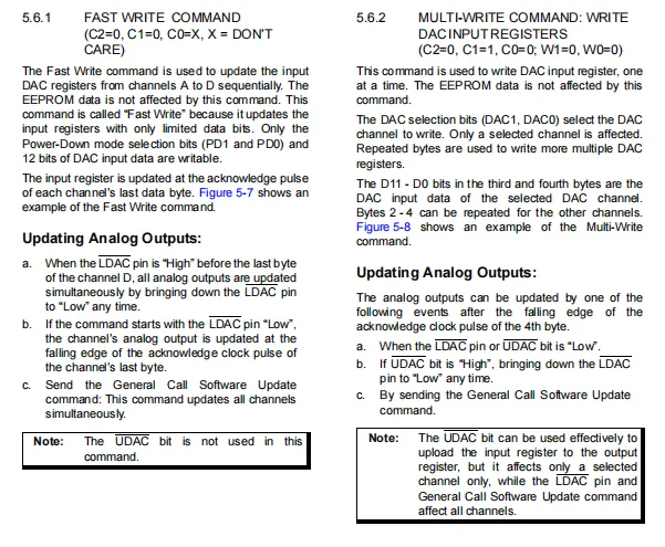
MCP4728 provides the fast write command (C2 = 0, C1 = 0) and the multi-channel write command (C2 = 0, C1 = 1): the fast write command can sequentially update the input registers of channels A to D, while the multi-channel write command allows individual channel selection for input register update; neither command affects the EEPROM, and output updates can be triggered synchronously via the LDAC pin or the general call command, offering an efficient and flexible write operation mode for multi-channel DAC control.
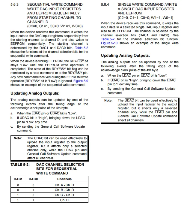
MCP4728 's sequential write command (C2 = 0, C1 = 1) can sequentially update the input registers of all channels starting from the specified channel and write to EEPROM, while the single write command (C2 = 0, C1 = 1;W1 = 1, W0 = 1) only operates the input register and EEPROM of the specified single channel. The outputs of both commands can trigger updates via the LDAC / UDAC pin or general call command, and the RDY / BSY pin can monitor the EEPROM write status, providing a flexible solution for precise single/multi-channel control.
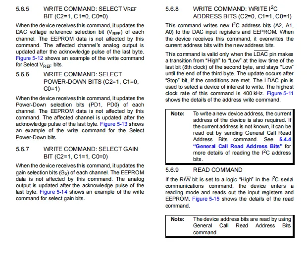
MCP4728 provides a rich set of configuration commands: it supports selection of internal/external reference voltage, gain setting (1/2x), power-down mode configuration, and also enables I²C address bit programming and register/ EEPROM reading, delivering flexible parameter configuration and status reading capabilities for multi-channel analog systems.
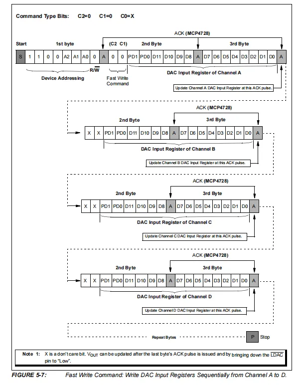
The fast write command of the MCP4728 (C2 = 0, C1 = 0) writes 12-bit DAC data and power-down configuration bits to channels A to D in sequence via the I²C bus. Each channel updates its input register after an acknowledge pulse, and finally all channel outputs can be updated synchronously by pulling the LDAC pin low, enabling efficient multi-channel analog voltage output.
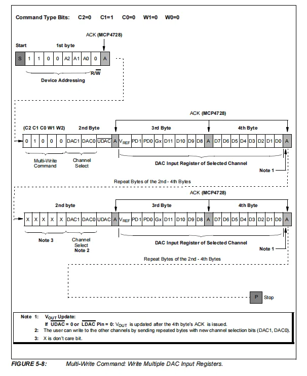
MCP4728 's multi-channel write command (C2 = 0, C1 = 1, C0 = 0) selects the specified channel via the I²C interface, writes 12-bit DAC data and reference/gain/power-down configuration, and supports repeated operations for multiple channels. Output updates are triggered by the LDAC / UDAC pin or general call command, providing flexible independent channel update capability for multi-channel analog control.
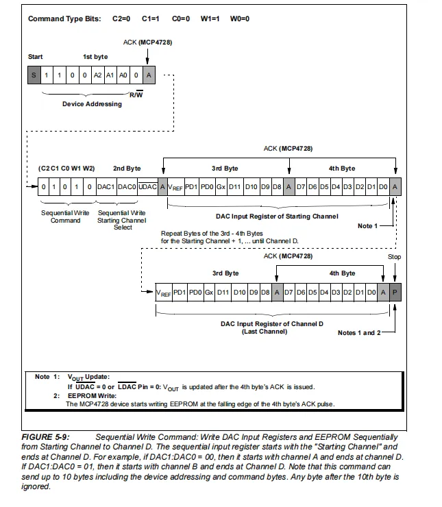
MCP4728 sequential write command (C2 = 0, C1 = 1, C0 = 0;W1 = 1, W0 = 0) can sequentially update the input registers of all subsequent channels starting from the specified starting channel, and batch write the configuration to EEPROM. The RDY / BSY pin can monitor the write status, and the output update is triggered by the LDAC / UDAC pin, providing efficient synchronous configuration and data persistence capabilities for multi-channel power-off save scenarios.
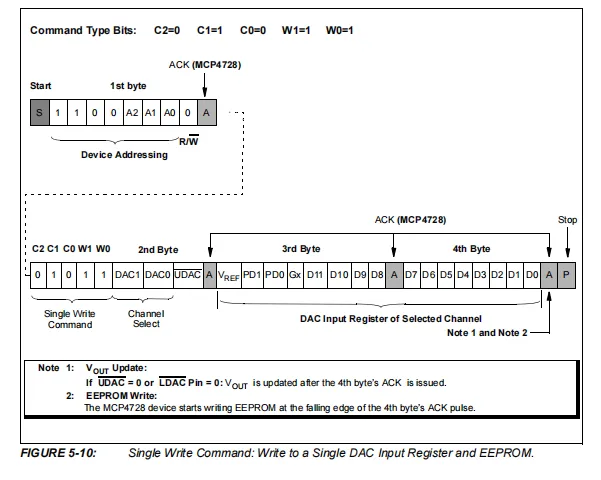
MCP4728 single write command (C2 = 0, C1 = 1, C0 = 0;W1 = 1, W0 = 1) allows selecting a specified channel, writing 12-bit DAC data and reference/gain/power-down configuration to the input register and EEPROM. Output update is triggered by the LDAC / UDAC pin, and the RDY / BSY pin can monitor the EEPROM write status, enabling precise single-channel control and power-off data retention.
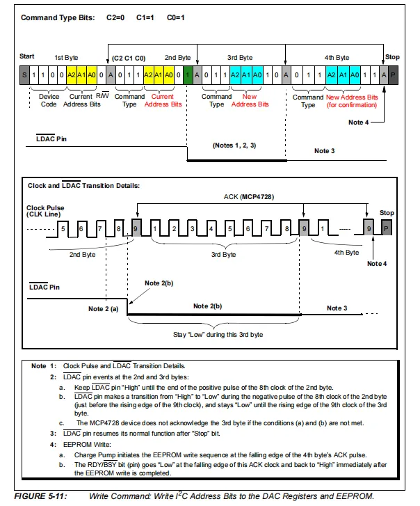
MCP4728 ’s I²C address write command (with C2 = 0, C1 = 1, C0 = 1) requires a level transition on the LDAC pin to write the new address bits to both the input register and the EEPROM, where they are retained even after power-off; the RDY / BSY pin can monitor the programming status, providing flexible address reconfiguration capability for multi-device bus systems.
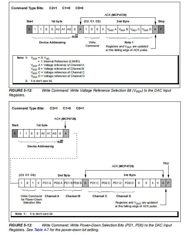
MCP4728 provides two key configuration commands: the reference selection command (C2 = 1, C1 = 0, C0 = 0) can configure each channel to use the internal 2.048V or external VDD as the reference voltage;the power-down mode command (C2 = 1, C1 = 0, C0 = 1) can independently set the power-down state of each channel. Both commands update the registers after the acknowledge pulse, and the outputs take effect synchronously, offering flexible configuration for low-power, high-precision multi-channel analog systems.
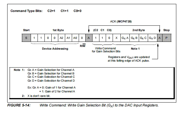
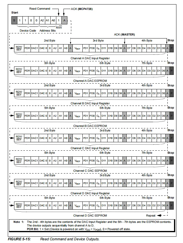
The MCP4728 provides a gain selection command (C2 = 1, C1 = 1, C0 = 0) that allows each channel to be independently configured for a gain of 1x or 2x, with outputs updated synchronously after an acknowledge pulse; it also supports a read command (R / W = 1) to sequentially read the input registers and EEPROM data of each channel, including configuration statuses such as reference, gain, and power-down, delivering flexible parameter configuration and status monitoring capabilities for multi-channel analog systems.
2.8 PCB Routing Notes
None.
III. Circuit Engineering
3.1 Circuit Source Engineering
To obtain the circuit source project, please follow the official account [Freak Embedded].
3.2 Module Usage Instructions
SCH_4-Channel DAC Module Based on MCP4728-V1.0.0_2026-03-27.pdf 2.8 MB
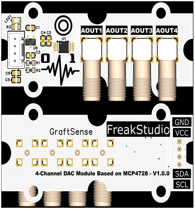
This module provides an I²C communication interface: it supports three communication modes including standard (100kbps), fast (400kbps) and high-speed (3.4Mbps), with a fixed device address consisting of the 1101 device code plus three programmable address bits (which can be written into EEPROM for power-off storage). It is compatible with 3.3V/5V logic levels, and can implement batch reset, wake-up and synchronous update for multiple devices via the general call command, providing efficient and flexible digital instruction interaction and parameter configuration capabilities for multi-channel analog control scenarios.
Here, we provide 4 SMA interfaces, which can be connected to SMA adapter cables to interface with signal input sources.
3.3 Application Experiment
Here, we use the GraftPort-RP2040 development board for testing, and the digital-to-analog conversion module based on the MCP4728 chip uses the I2C0 interface to communicate with the main controller.
Here, we first use the HY2.0-4P cable to connect the module to the GraftPort-RP2040 development board's I2C interface, and meanwhile connect the AOUT2 corresponding SMA port of the analog output interface to SMA to red-black Dupont wires to GP26 and GND:
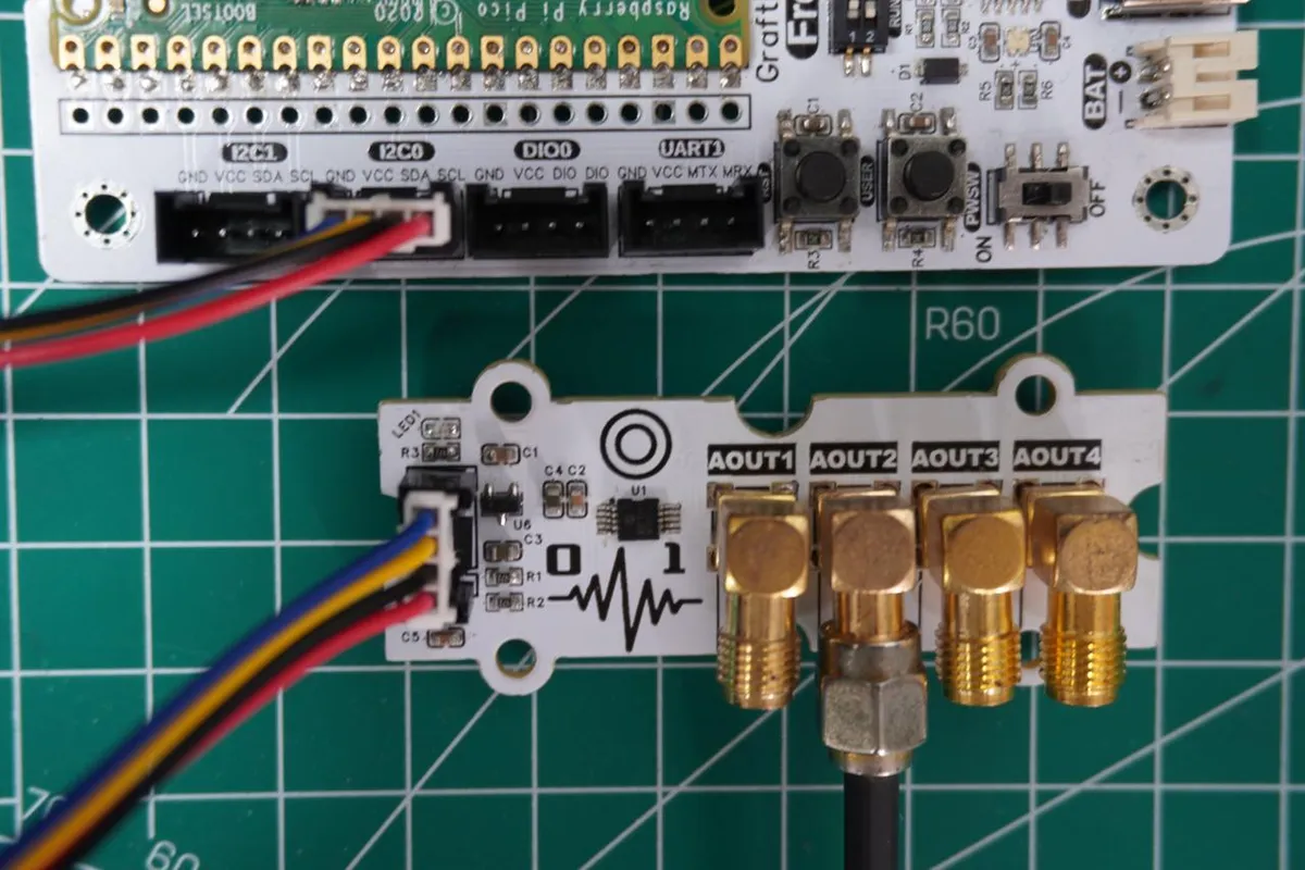
The module connections are shown in the following table:
Development Board Pins | Module Pins | Description |
Pin 4 |
|
|
Pin 5 |
|
|
Here, we need to search for the relevant driver packages on uPyPI: https://upypi.net/zh/
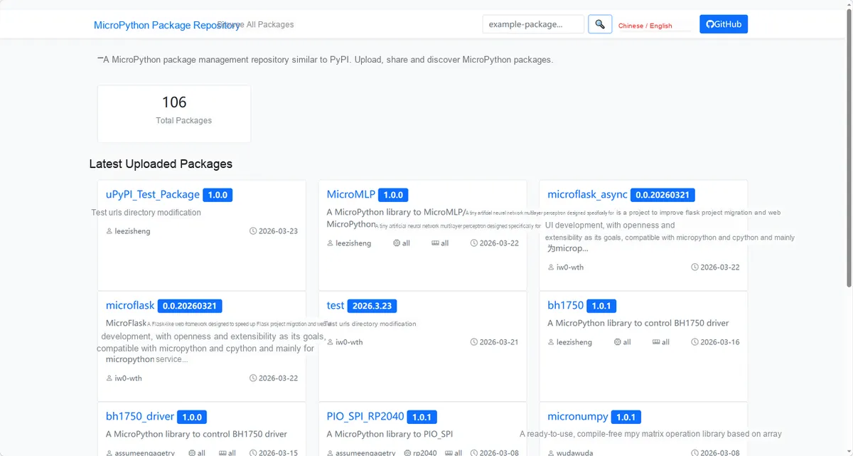
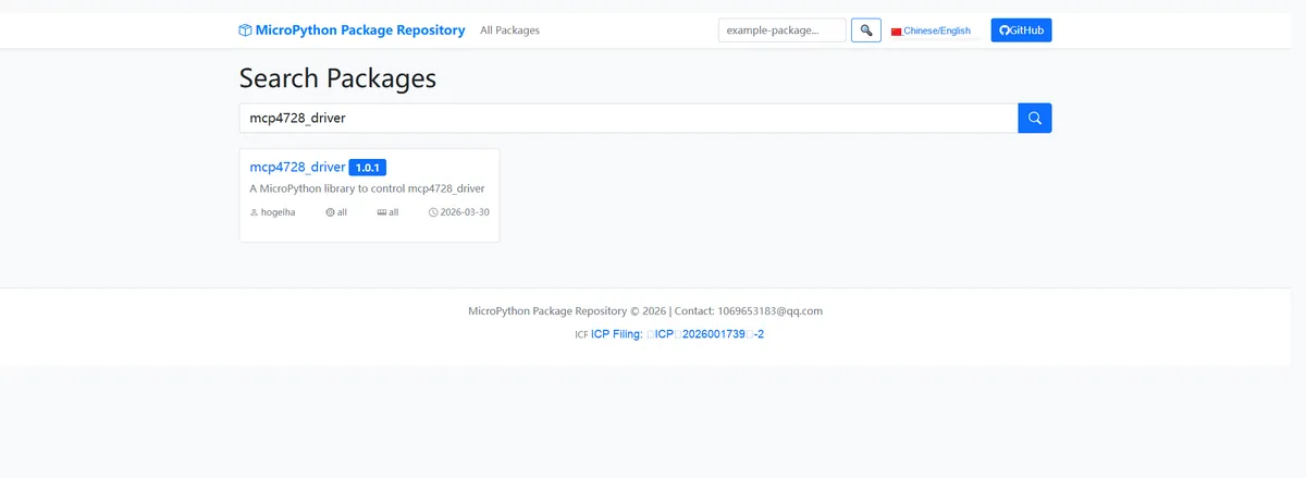
Enter mcp4728_driver to search, and the following will be displayed:
Click to copy the local installation command:
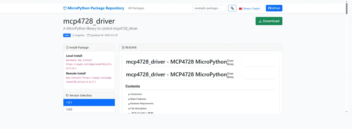
Import the module driver library code via the mip tool. Below are the usage commands for the mpremote tool:
mpremote mip install https://upypi.net/pkgs/mcp4728_driver/1.0.0After importing the MicroPython driver code for the MCP4728 chip-based digital-to-analog conversion module , copy the following main.py code into our project:
# Python env   : MicroPython v1.23.0
# -*- coding: utf-8 -*-
# @Time    : 2026/3/16 2:00 PM
# @Author  : hogeiha
# @File    : main.py
# @Description : Verify the output function of the MCP4728 four-channel DAC module, reading the output voltage of DAC channel B through the ADC to confirm that the value, reference voltage, gain and other parameter settings take effect

# ======================================== Import Modules =========================================

import time
from machine import Pin, I2C, ADC
import mcp4728

# ======================================== Global Variables ============================================
# I2C SCL pin
I2C_SCL_PIN = 5
# I2C SDA pin
I2C_SDA_PIN = 4
# I2C communication frequency
I2C_FREQ = 400000
# MCP4728 target I2C address
TARGET_DAC_ADDR = 0x60

# ======================================== Functions ============================================


def verify_dac_output():
    """
    Verify the output function of DAC channel B by setting different values, reference voltages and gains, reading the ADC value and converting it to the actual voltage
    Args: None

    Raises: None

    Notes: After setting the DAC value, a short delay is needed to ensure the output voltage is stable before reading the ADC value

    ==========================================
    Verify the output function of DAC channel B, set different values, reference voltages and gains, read ADC values and convert to actual voltage
    Args:None

    Raises:None

    Notes:A short delay is required after setting the DAC value to ensure the output voltage is stable before reading the ADC value
    """
    # Example 1: Set channel B to the 12-bit maximum value 4095, corresponding to full-scale output voltage
    dac1.b.value = 4095
    # Delay 0.1 seconds, wait for the DAC output voltage to stabilize
    time.sleep(0.1)
    # Read the ADC value, range 0-65535
    adc_val = adc.read_u16()
    # Convert the ADC value to the actual voltage, assuming the ADC reference voltage is 3.3V
    voltage = (adc_val / 65535) * 3.3
    # Print the DAC setting value, ADC reading and actual voltage (English output)
    print(f"DAC Channel B set to 4095 → ADC reading: {adc_val} → Actual voltage: {voltage:.2f}V")

    # Example 2: Set channel B to the middle value 2048
    dac1.b.value = 2048
    # Delay 0.1 seconds, wait for the DAC output voltage to stabilize
    time.sleep(0.1)
    # Read the ADC value
    adc_val = adc.read_u16()
    # Convert to the actual voltage
    voltage = (adc_val / 65535) * 3.3
    # Print related information (English output)
    print(f"DAC Channel B set to 2048 → ADC reading: {adc_val} → Actual voltage: {voltage:.2f}V")

    # Example 3: Set channel B output using a normalized value (0.0-1.0)
    dac1.b.normalized_value = 0.5
    # Delay 0.1 seconds, wait for the DAC output voltage to stabilize
    time.sleep(0.1)
    # Read the ADC value
    adc_val = adc.read_u16()
    # Convert to the actual voltage
    voltage = (adc_val / 65535) * 3.3
    # Print related information (English output)
    print(f"DAC Channel B set to 0.5 (normalized) → ADC reading: {adc_val} → Actual voltage: {voltage:.2f}V")

    # Example 4: Change the reference voltage and gain of channel B, then verify the output
    # Set the channel B reference voltage to internal 2.048V
    dac1.b.vref = 1
    # Set the channel B gain to 2x (only effective with the internal reference voltage)
    dac1.b.gain = 2
    # Set the channel B value to 4095
    dac1.b.value = 4095
    # Delay 0.1 seconds, wait for the DAC output voltage to stabilize
    time.sleep(0.1)
    # Read the ADC value
    adc_val = adc.read_u16()
    # Convert to the actual voltage
    voltage = (adc_val / 65535) * 3.3
    # Print related information (English output)
    print(f"DAC Channel B (Vref=2.048V, gain=2) → Actual voltage: {voltage:.2f}V")


# ======================================== Custom Classes ============================================

# ======================================== Initialization configuration ===========================================

# System startup delay of 3 seconds to ensure hardware initialization is complete
time.sleep(3)
# Print initialization complete message (English)
print("FreakStudio: MCP4728 DAC output verification via ADC")

# Initialize the I2C bus, with the variable name changed to i2c_bus to match the example code style
i2c_bus = I2C(0, scl=Pin(I2C_SCL_PIN), sda=Pin(I2C_SDA_PIN), freq=I2C_FREQ)

# Added complete I2C scan logic, strictly matching the example code style
# Start scanning for devices on the I2C bus
devices_list: list[int] = i2c_bus.scan()
print("START I2C SCANNER")

# Check the I2C device scan result
if len(devices_list) == 0:
    print("No i2c device !")
    raise SystemExit("I2C scan found no devices, program exited")
else:
    print("i2c devices found:", len(devices_list))

    # Iterate over the address list to initialize the target DAC module
    dac1 = None  # Initialize DAC variable
    for device in devices_list:
        if device == TARGET_DAC_ADDR:
            print("I2c hexadecimal address:", hex(device))
            try:
                # Initialize the MCP4728 DAC module
                dac1 = mcp4728.MCP4728(i2c_bus=i2c_bus, address=TARGET_DAC_ADDR)
                print("Target DAC (MCP4728) initialization successful")
                break
            except Exception as e:
                print(f"DAC Initialization failed: {e}")
                continue
    # Raise an exception when no target DAC address is found
    if dac1 is None:
        raise Exception("No MCP4728 DAC found on I2C bus")

# Initialize the ADC object, specifying pin 26 for reading the analog voltage output by the DAC
adc = ADC(Pin(26))

# ========================================  Main Program  ============================================

# Run the DAC output verification function
verify_dac_output()

# Read and print the power mode, reference voltage and gain parameters of channel B (English output)
print("\nCurrent Channel B power mode: ", dac1.b.pdm)
print("Current Channel B reference voltage: ", dac1.b.vref)
print("Current Channel B gain: ", dac1.b.gain)
In the above code, we use the ADC to acquire the output voltage of DAC Channel B. By configuring different digital values, normalized values, reference voltages and gain parameters, we verify the output function of the DAC, calculate and print the actual output voltage, and finally read and display the operating parameters of Channel B, thus completing a comprehensive verification of the output performance of the MCP4728 module.
Burn the code, open the terminal, and the output is as follows:
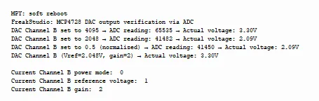
It can be seen that it is working properly.
IV. Drivers
mcp4728_driver-1.0.1.zip 18 KB
5. BOM & Recommended Alternative Parts
None.
6. Revision History
Document Version | Date of Revision | Modifier | Modified Content |
v1.0 | 2026-03-27 | Ling Gaoxing | Initialize the document |
v1.0.1 | 2026-04-05 | Li Zisheng | The homepage photo has not been taken, the production files have not been exported yet, and all other items have been sorted out completely. |
v1.0.2 | 2026-04-21 | Li Zisheng | The production documents have not been exported yet, while all the others have been sorted out completely. |
v1.1 | 2026-04-23 | Xin Ruili | Create an open version of the document, based on the internal document version v1.0.2. |
VII. Relevant Materials
7.1 Chip Datasheet
C478093_DAC Chip_MCP4728T-E-UN_Datasheet_WJ97843.PDF 2.9 MB
7.2 Unique Icons for PCB Silk Screen