Contents
- I. Module Introduction
- II. Introduction to Main Chips
- 2.1 Chip Overview
- 2.2 Pin Definition
- 2.3 Functional Block Diagram
- 2.4 Performance Parameters
- 2.5 Reference Circuit
- 2.6 Chip Configuration
- 2.7 Communication Interfaces and Related Protocols
- 2.8 PCB Routing Precautions
- III. Circuit Engineering
- 3.1 Circuit Source Engineering
- 3.2 Module Usage Instructions
- 3.3 Application Experiment
- IV. Drivers
- 5. BOM & Recommended Alternative Parts
- VI. Revision History
- 7. Relevant Materials
- 7.1 Chip Datasheet
- 7.2 Unique Icons for PCB Silk Screen
I. Module Introduction
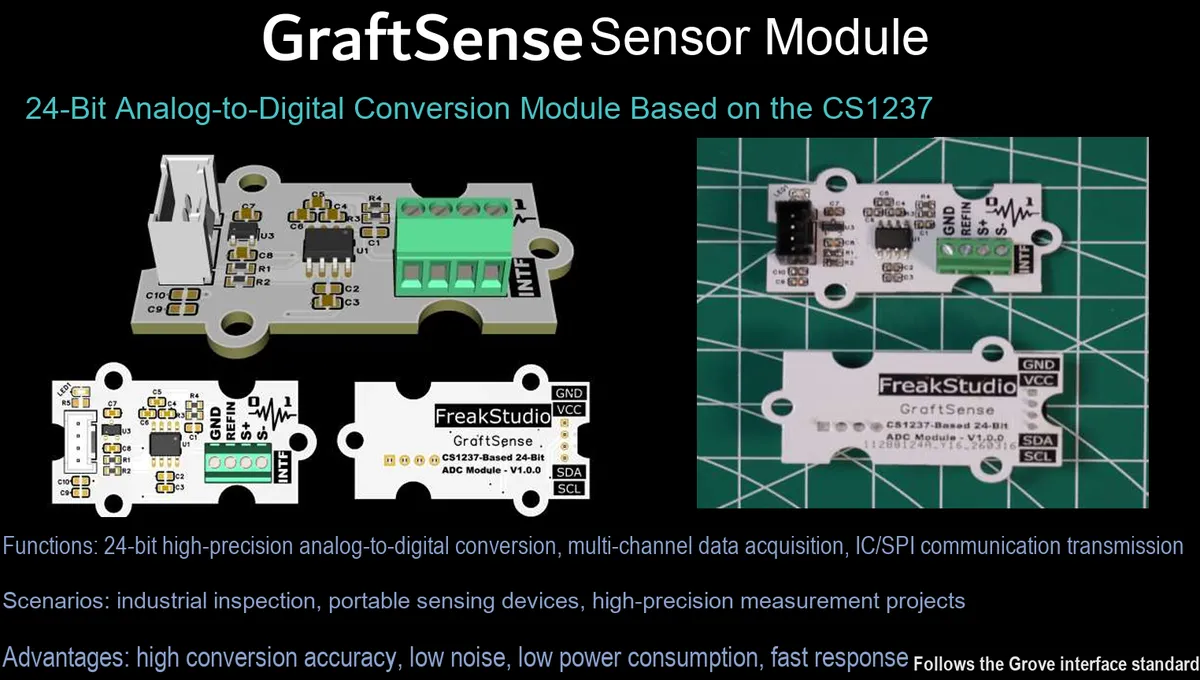
24-bit Analog-to-Digital Conversion Module Based on CS1237, adopting the CS1237 from Chipsea Technologies CS1237 24-bit high-precision Σ-Δ type ADC chip solution, with built-in programmable gain amplifier and on-chip oscillator, supporting differential input, and a maximum sampling rate of 1280 SPS;The communication interface adopts Chipsea's proprietary two-wire protocol (SCLK + DRDY / DOUT), and is equipped with a 5V-to-3.3V LDO voltage regulator circuit and power filter circuit, compatible with 3.3V level. The 24-bit resolution delivers extremely low noise and ultra-high linearity, making it suitable for industrial-grade signal acquisition scenarios such as high-precision weighing and pressure sensing, providing the system with accurate and efficient high-precision analog signal digitization capability.
II. Introduction to Main Chips
CS1237 is a 24-bit Σ-Δ high-precision ADC chip launched by Chipsea Technologies. It integrates a programmable gain amplifier and an on-chip oscillator, supports differential input, operates with a supply voltage of 2.7V to 5.5V, features a maximum sampling rate of 1280 SPS, adopts a proprietary two-wire Communication Protocol, and is suitable for low-noise analog signal acquisition scenarios such as high-precision weighing and pressure sensing.
2.1 Chip Overview
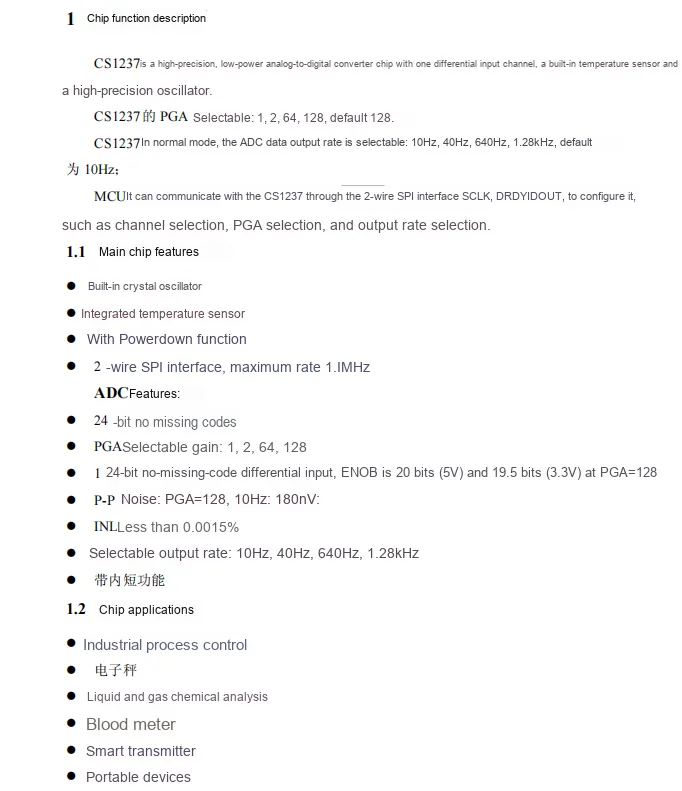
CS1237 is a 24-bit high-precision low-power Σ-Δ type ADC with built-in crystal oscillator, temperature sensor and programmable gain amplifier (PGA optional at 1/2/64/128), supporting 1 differential input channel with selectable sampling rate from 10Hz to 1.28kHz, communicating via 2-wire SPI interface. It features extremely low noise and ultra-high linearity, making it suitable for high-precision signal acquisition scenarios such as electronic scales and industrial control.
2.2 Pin Definition
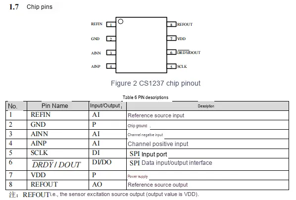
2.3 Functional Block Diagram
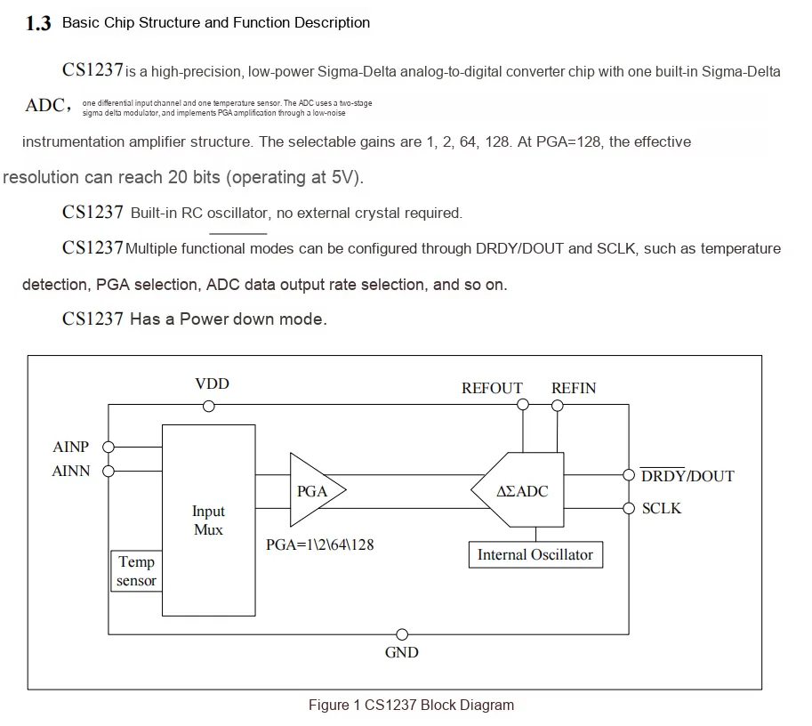
2.4 Performance Parameters
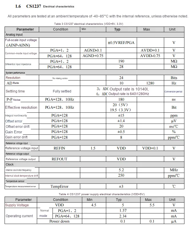

Powered by a single supply of 2.7V~5.5V, compatible with 3.3V/5V, 24-bit no-missing-code resolution, PGA with selectable gain from 1 to 128, sampling rate ranging from 10Hz to 1280SPS, PGA = 128, the peak-to-peak noise is only 180nV at 10Hz, INL < 0.0015%, built-in temperature sensor with ±3℃ error, normal operating current of 1.26mA~2.34mA and power-down current of only 0.1μA, providing stable and reliable performance guarantee for high-precision and low-power signal acquisition.
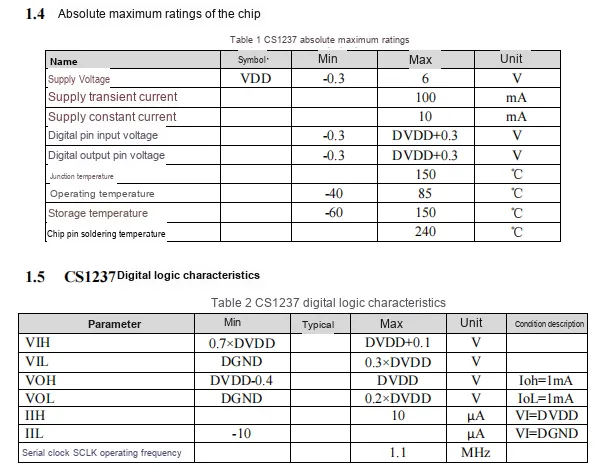
CS1237 's absolute maximum ratings and digital logic characteristics: power supply voltage range - 0.3V~6V, digital pin level is compatible with 0.7× DVDD high level and 0.3× DVDD low level, SCLK maximum operating frequency 1.1MHz, operating temperature -40℃~85℃, which provides safe and reliable electrical boundaries and communication timing guarantee for chip design and application.
2.5 Reference Circuit
None.
2.6 Chip Configuration
None.
2.7 Communication Interfaces and Related Protocols
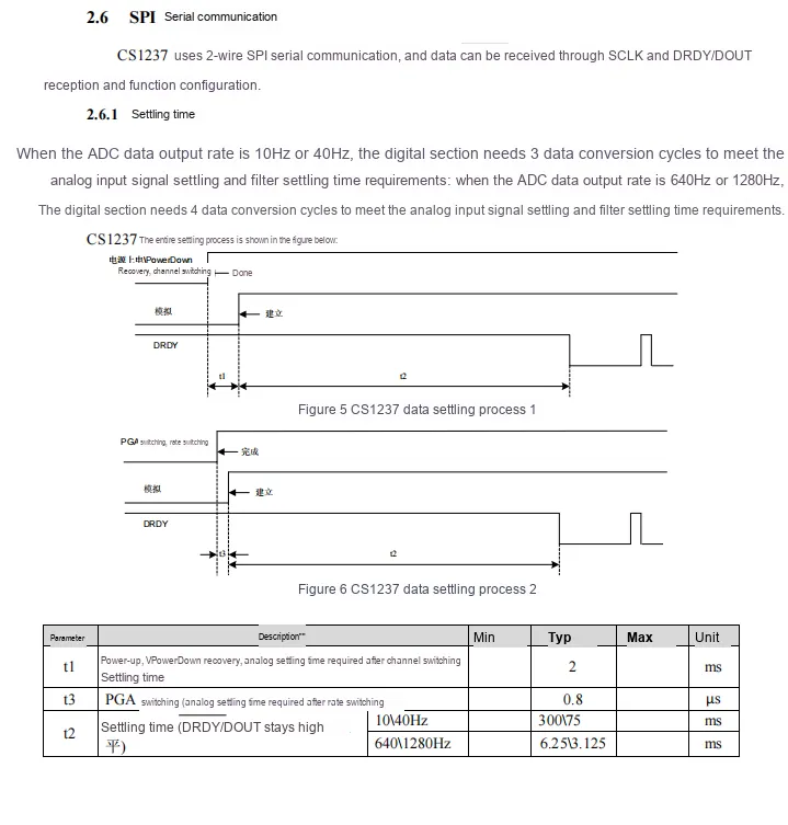
CS1237 adopts 2-wire SPI serial communication (SCLK + DRDY / DOUT). After power-on or channel switching, the analog signal requires a settling time of 2ms; after PGA or rate switching, a settling time of 0.8μs is required. When the data output rate is 10Hz/40Hz, 3 conversion cycles are needed for data settling, while 4 conversion cycles are required at 640Hz/1280Hz, which meets the timing and stability requirements for high-precision acquisition.
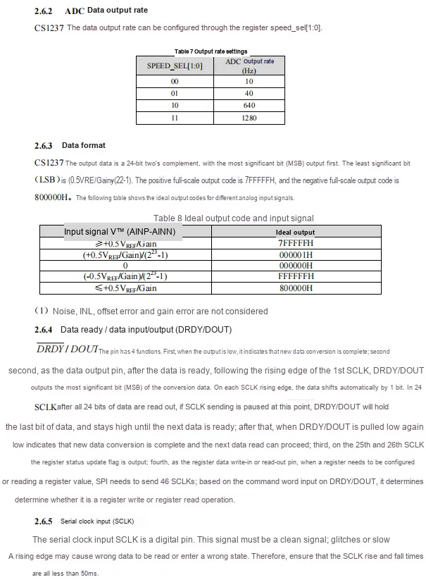
CS1237 configures the speed_sel[1:0]register to set the output rate of the ADC within 10Hz~1280Hz; the output is in 24-bit two's complement format with the most significant bit transmitted first, and it communicates via the two-wire protocol consisting of DRDY/DOUT and SCLK. The DRDY / DOUT pin integrates multiple functions including data ready indication, ADC data output, and register configuration. The SCLK requires clean and fast edges to ensure reliable communication, making it suitable for high-precision, low-noise signal acquisition scenarios.
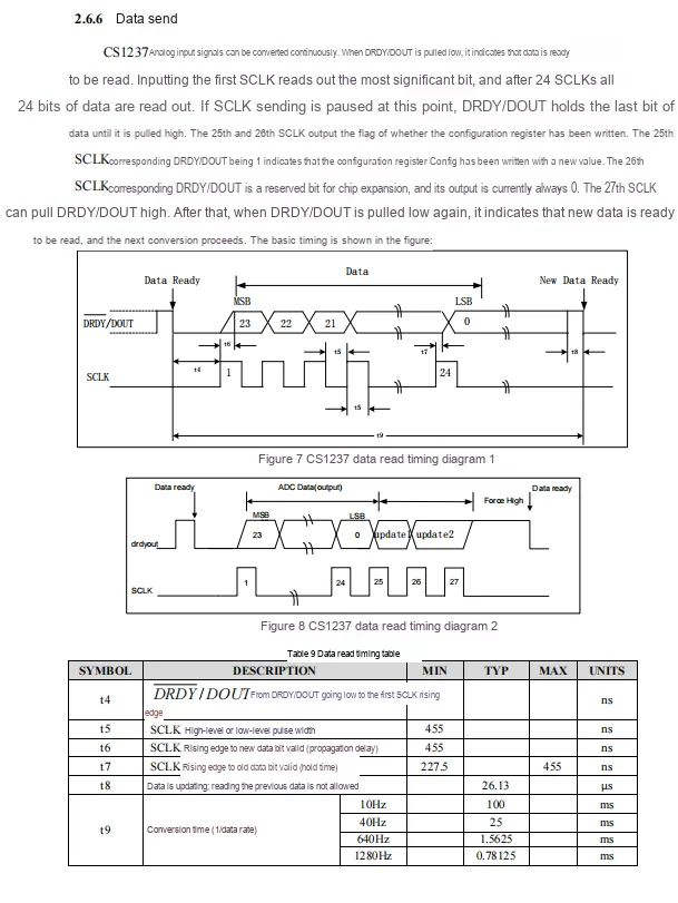
CS1237 adopts DRDY / DOUT and SCLK two-wire timing to complete 24-bit data reading. After DRDY/DOUT is pulled low, two's complement data is output on the 24 rising edges of SCLK, the register update flag is output on the 25th to 26th SCLK, and the transmission ends when the 27th SCLK is pulled high. The timing parameters strictly constrain the data setup and hold time, and the conversion cycle corresponds to 100ms to 0.78ms as the sampling rate ranges from 10Hz to 1280Hz, providing efficient and reliable timing interaction capability for high-precision signal acquisition.
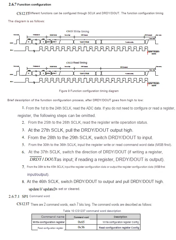
CS1237 implements functional configuration via the two-wire interface consisting of SCLK and DRDY / DOUT. After completing 24-bit ADC data reading, a 7-bit command word (write configuration register 0x65 / read configuration register 0x56) can be sent via the 25th to 46th SCLK to complete register read/write and function mode setting, providing flexible and efficient configuration interaction capability for high-precision acquisition scenarios.
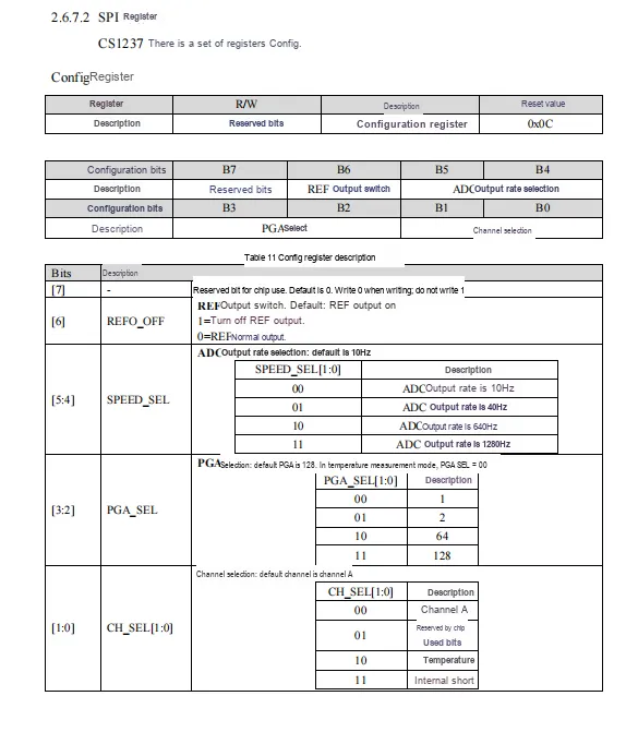
CS1237 's Config register is an 8-bit configuration register with a reset value of 0x0C; bit [7] is a reserved bit that defaults to 0 when written, bit [6] controls the REF output switch, bits [5:4]SPEED_SEL can select a sampling rate of 10Hz/40Hz/640Hz/1280Hz, bits [3:2]PGA_SEL configure a gain of 1/2/64/128, and bits [1:0]CH_SEL select channel A, temperature or internal short detection, enabling precise configuration of the chip' s acquisition parameters.
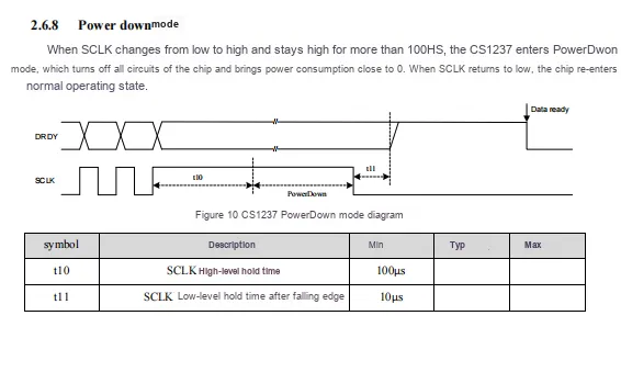
CS1237 Power down mode can be triggered by pulling SCLK high and holding it for more than 100μs; at this point, the chip shuts down all circuits, and the power consumption drops to approximately 0.1μA. When SCLK is pulled low and held for at least 10μs, the chip resumes normal operation mode, providing efficient energy-saving control capability for portable low-power devices.
2.8 PCB Routing Precautions
None.
III. Circuit Engineering
3.1 Circuit Source Engineering
To obtain the source code of the circuit, please follow the official account [Freak Embedded]
3.2 Module Usage Instructions
The schematic diagram of this module is shown below:
SCH_24-bit ADC Module Based on CS1237-V1.0.0_2026-03-27.pdf 2.2 MB
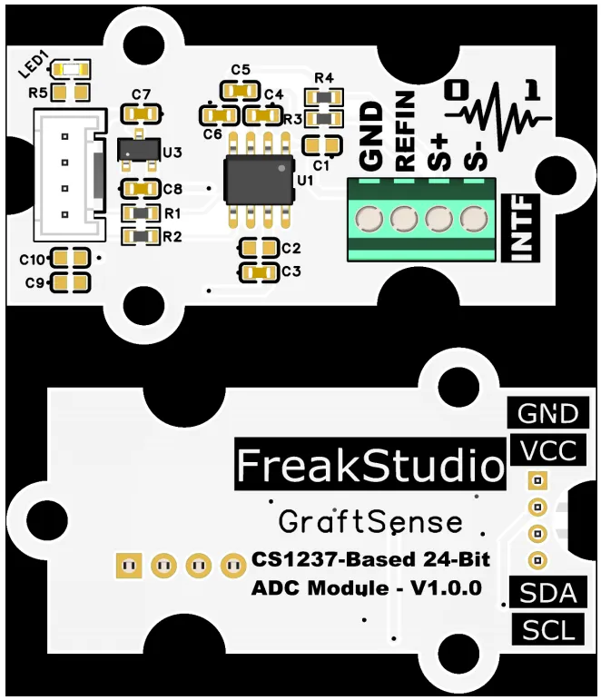
This module provides a proprietary two-wire communication interface of Chipsea that adopts the SCLK + DRDY / DOUT protocol with a maximum communication rate of 1.1MHz. Both DOUT and SCLK are connected in series with a 100Ω resistor for current limiting protection to prevent signal overshoot; it is compatible with 3.3V level, and allows flexible configuration of PGA gain, sampling rate and channel selection through this interface, capable of stably reading 24-bit high-precision ADC data. It is suitable for industrial-grade low-noise signal acquisition scenarios such as high-precision weighing and pressure sensing, providing the system with accurate and efficient analog-to-digital signal interaction capabilities.
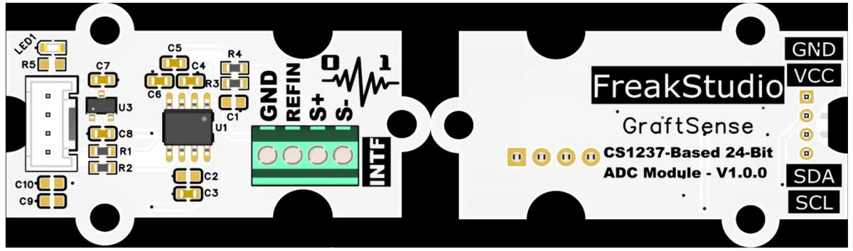
INF The functions of the interface pins are as follows:
| Signal Label | Core Function | Additional notes |
|---|---|---|
| S⁻ | Sensor differential signal negative input | Connects to the negative signal output of the load cell / strain gauge sensor, corresponding to AINN (pin 3) of the CS1237. Provides the negative differential input signal to the ADC to acquire the weak voltage output by the sensor |
| S⁺ | Sensor differential signal positive input | Connects to the positive signal output of the load cell / strain gauge sensor, corresponding to AINP (pin 4) of the CS1237. Provides the positive differential input signal to the ADC and forms a differential input pair with S⁻, which effectively suppresses common-mode interference |
| REFIN | Reference voltage input / output | 1. Can connect an external high-precision reference source to provide a stable reference voltage for the CS1237 ADC and improve measurement accuracy; 2. Can output the CS1237 internal reference (REFOUT) to provide excitation voltage for the sensor bridge; 3. In the schematic, REFIN (pin 1) and REFOUT (pin 8) of the CS1237 are shorted together, so this pin can both input and output |
| GND | Common reference ground (power / signal ground) | Unified potential reference of the module. Connects to the system power ground and sensor ground, provides a common ground reference for the ADC, LDO, sensor and other circuits, and also suppresses common-mode interference to ensure signal integrity |
3.3 Application Experiment
Here, we use the GraftPort-RP2040 development board for testing. The 24-bit analog-to-digital conversion module based on CS1237 uses the I2C interface to communicate with the main controller.
Here, we first use the HY2.0-4P cable to connect the module to the GraftPort-RP2040 development board's I2C0 interface:
The module connections are shown in the following table:
Development Board Pins | Module Pins | Description |
Pin 4 |
|
|
Pin 5 |
|
|
The INF interface terminals of the module are connected as follows:
| Silkscreen Label | Function definition | Current Wiring |
|---|---|---|
| GND | System common ground (power / signal ground) | Connected to DC power supply GND (common ground) |
| REFIN | ADC reference voltage input | Floating (using internal reference) |
| S+ | Differential analog input positive terminal (AIN+) | Connected to DC power supply 1.2V |
| S- | Differential analog input negative terminal (AIN-) | Connected to DC power supply GND |
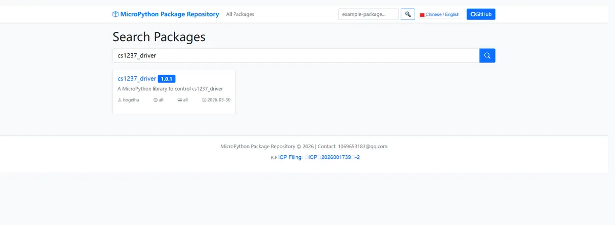
Here, we need to search for the relevant driver packages on uPyPI: https://upypi.net/zh/
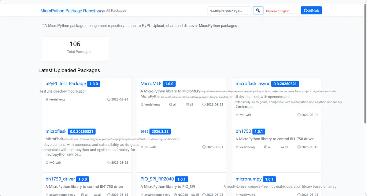
Enter cs1237_driver to search, and the following will be displayed:
Click to copy the local installation command:
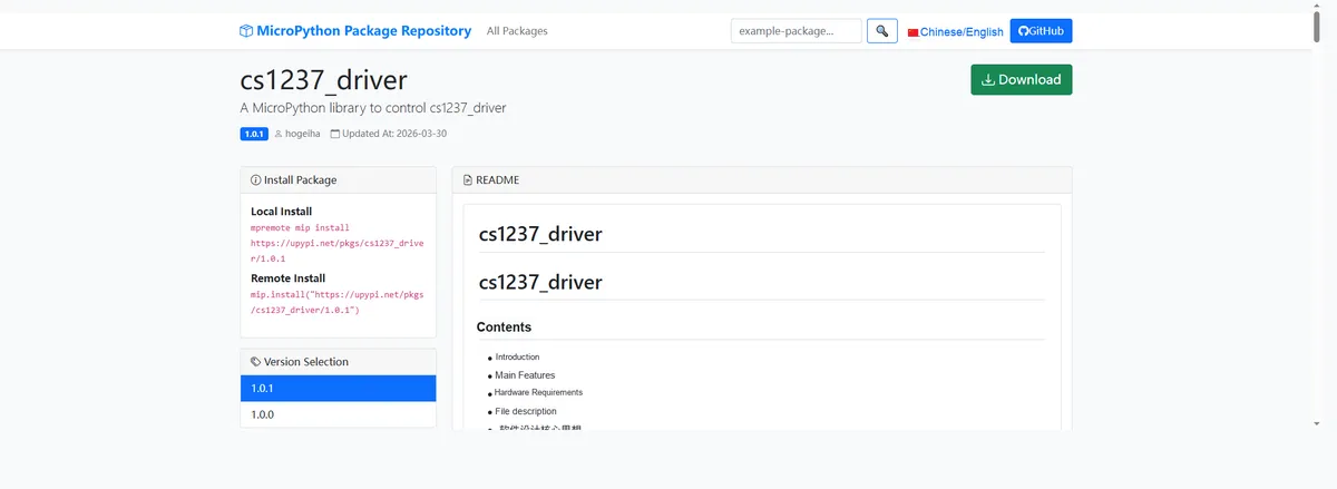
Import the module driver library code via the mip tool. Below are the usage commands for the mpremote tool:
mpremote mip install https://upypi.net/pkgs/cs1237_driver/1.0.0Import the 24-bit analog-to-digital conversion module based on CS1237 - MicroPython driver code, then copy the following main.py code into our project:
# Python env   : MicroPython v1.23.0
# -*- coding: utf-8 -*-
# @Time    : 2026/3/17 4:52 PM
# @Author  : hogeiha
# @File    : main.py
# @Description : Usage example for the CS1237/CS1238 series ADC chip driver, covering basic reading, buffered reading, temperature calibration, power management and other functions

# ======================================== Import Modules =========================================
import array
import time
from machine import Pin
from cs1237 import CS1237

# ======================================== Global variables =========================================

# ======================================== Functions ============================================
def adc_to_voltage(adc_value):
    # At gain=1, full scale 8388607 = 1.25V
    return (adc_value / 8388607) * 1.25

def demo_cs1237_basic():
    print("\n=== CS1237 Basic Read Example ===")
    try:
        # ✅ Fixed gain of 1
        adc = CS1237(clock=CLK_PIN, data=DATA_PIN, gain=1, rate=10, channel=0)
        print(f"Chip initialization configuration: {adc}")

        gain, rate, channel = adc.get_config()
        print(f"Current configuration - Gain: {gain}, Sample rate: {rate}Hz, Channel: {channel}")

        print("Start reading ADC data:")
        for i in range(5):
            try:
                value = adc.read()
                voltage = adc_to_voltage(value)
                print(f"Read {i + 1} times: {value}  →  Voltage: {voltage:.3f} V")
                time.sleep(0.5)
            except OSError as e:
                print(f"Read failed: {e}")

        # ✅ Keep gain at 1 when changing the configuration too
        print("\nModify configuration (Gain 1, Sample rate 40Hz)...")
        adc.config(gain=1, rate=40)
        gain, rate, channel = adc.get_config()
        print(f"Modified configuration - Gain: {gain}, Sample rate: {rate}Hz, Channel: {channel}")

        value = adc.read()
        voltage = adc_to_voltage(value)
        print(f"Read value under new configuration: {value}  →  Voltage: {voltage:.3f} V")

    except (ValueError, TypeError, OSError) as e:
        print(f"Initialization/Read failed: {e}")


def demo_buffered_read():
    print("\n=== Buffered Batch Read Example ===")
    try:
        # ✅ gain=1 must be added here
        adc = CS1237(CLK_PIN, DATA_PIN, gain=1)
        buffer = array.array("i", [0] * 10)

        print("Start buffered reading 10 data...")
        adc.read_buffered(buffer)

        while not adc.data_acquired:
            time.sleep(0.01)

        print("Buffered read results:")
        for idx, val in enumerate(buffer):
            voltage = adc_to_voltage(val)
            print(f"Data {idx + 1}: {val}  →  Voltage: {voltage:.3f} V")

    except (ValueError, TypeError, OSError) as e:
        print(f"Buffered read failed: {e}")


def demo_temperature_calibration():
    print("\n=== Temperature Calibration and Read Example ===")
    try:
        # ✅ gain=1 must be added here
        adc = CS1237(CLK_PIN, DATA_PIN, gain=1)

        print("Start temperature calibration (Current temperature 25℃)...")
        adc.calibrate_temperature(temp=25.0)
        print(f"Calibration reference value: {adc.ref_value}, Reference temperature: {adc.ref_temp}℃")

        print("Read current temperature...")
        for i in range(3):
            try:
                temp = adc.temperature()
                print(f"Temperature read {i + 1} times: {temp:.2f}℃")
                time.sleep(0.5)
            except OSError as e:
                print(f"Temperature read failed: {e}")

    except (ValueError, TypeError, OSError) as e:
        print(f"Temperature function failed: {e}")


def demo_power_management():
    print("\n=== Power Management Example ===")
    try:
        # ✅ gain=1 must be added here
        adc = CS1237(CLK_PIN, DATA_PIN, gain=1)

        value = adc.read()
        voltage = adc_to_voltage(value)
        print(f"Read value before power down: {value}  →  Voltage: {voltage:.3f} V")

        print("Enter power down mode...")
        adc.power_down()
        time.sleep(2)

        print("Wake up chip...")
        adc.power_up()
        time.sleep(0.1)

        value = adc.read()
        voltage = adc_to_voltage(value)
        print(f"Read value after wake up: {value}  →  Voltage: {voltage:.3f} V")

    except (ValueError, TypeError, OSError) as e:
        print(f"Power management failed: {e}")


# ======================================== Initialization configuration ===========================================
time.sleep(3)
print("FreakStudio: CS1237 ADC driver demo")

CLK_PIN = Pin(5, Pin.OUT)
DATA_PIN = Pin(4, Pin.IN)

# ========================================  Main Program  ============================================
if __name__ == "__main__":
    demo_cs1237_basic()
    demo_buffered_read()
    demo_temperature_calibration()
    demo_power_management()
    print("\n=== All examples executed completed ===")
Burn the code, open the terminal, and the output is as follows:
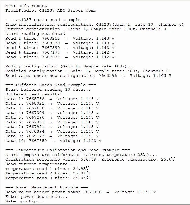
Here, we demonstrate the basic reading, buffering, temperature calibration and power management functions of the module.
IV. Drivers
cs1237_driver-1.0.2.zip 16 KB
5. BOM & Recommended Alternative Parts
None.
VI. Revision History
Document Version | Date Modified | Modifier | Modify Content |
v1.0 | 2026-03-27 | Ling Gaoxing | Initialize the document |
v1.0.1 | 2026-04-21 | Li Zisheng | The production documents have not been exported yet, and all the rest have been sorted out. |
v1.1 | 2026-04-29 | Xin Ruili | Create an open version of the document, based on the internal document version v1.0.1. |
7. Relevant Materials
7.1 Chip Datasheet
CS1237.pdf 599 KB
7.2 Unique Icons for PCB Silk Screen