
Contents
- 1. Hardware Explanation
- 1.1 Basic Structure of PIO Peripherals
- 1.2 Programming Model of PIO and Working Principle of finite-state machine
- 1.3 PIO Assembly Syntax
- 1.4 PIO Instruction Set
- 1.5 Detailed Explanation of PIO Functions and Features
- 1.6 Registers Related to PIO Control on Raspberry Pi Pico
- 2. Software Control Method
- 2.1 Constructor of the rp2.StateMachine Class
- 2.2 Other Methods of the rp2.StateMachine Class
- 2.3 Constructor Method of the rp2.PIO Class
- 2.4 Other Methods of the rp2.PIO Class
- 2.5 Function for Assembling PIO Assembly Programs
- 2.6 PIO Instructions in MicroPython
- 3. Application Examples
- 3.1 Flashing the Onboard LED with PIO Control
- 3.2 PIO Using Interrupts
- 3.3 PIO uses exec to execute instructions in the instr register
- 3.4 PIO Control of WS2182 Colorful Lights
- 3.5 PIO Control of Stepper Motors
- 3.6 Implementing UART Communication with PIO
- 3.7 Implementing SPI Communication with PIO
- References
- Version Record
Mind Map - Instruction Section
1. Hardware Explanation
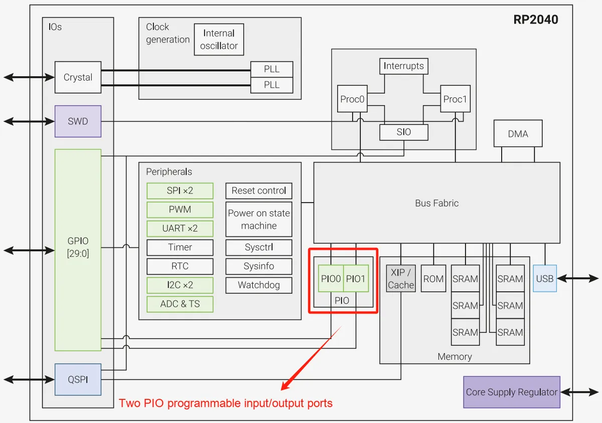
It is not difficult to see that for the RP2040 onboard the Raspberry Pi Pico board, its communication peripheral resources are very limited. When the number of communication peripherals we need to use is greater than the number of communication peripherals available on the Raspberry Pi Pico (for example, requiring four UARTs), or when the Communication Protocol we need is not supported by the hardware on the Raspberry Pi Pico (for example, VGA video output), in addition to using GPIO software to simulate and implement the communication interface, we can also select the PIO programmable input/output interface.
The PIO (Programmable Input/Output) is a dedicated peripheral of the RP2040 microcontroller. The term "programmable input/output" means that it can process data input to or output from specific GPIO pins using preconfigured operations without requiring intervention from the RP2040's CPU.It can implement a variety of different communication interfaces/peripherals. In fact, we can regard PIO as another simple and independent microcontroller inside the RP2040 chip. By writing a simple assembly program into the PIO block, multiple communication interfaces can be implemented. Meanwhile, compared with the GPIO software-emulated Communication Protocol, it hardly occupies CPU resources and features a high operating speed.
Currently, the PIO peripheral can implement the following Communication Protocols: 8080 and 6800 parallel buses, I2C, 3-pin I2S, SDIO, SPI, DSPI, QSPI, UART, DPI or VGA (via a resistive DAC).
1.1 Basic Structure of PIO Peripherals
The RP2040 features two identical PIO peripherals, each of which is independently connected to the AHB lite bus, GPIO pins, and interrupt controller:
- AHB Lite bus: enables high-speed data interaction between PIO and the main CPU of RP2040 as well as on-chip memory;
- GPIO pins: serve as the physical interfaces for the PIO to perform input/output operations with external devices;
- Interrupt controller: Implements the function of the PIO sending interrupt requests to the main CPU to complete event synchronization.
The structural diagram of a single PIO peripheral is shown below:
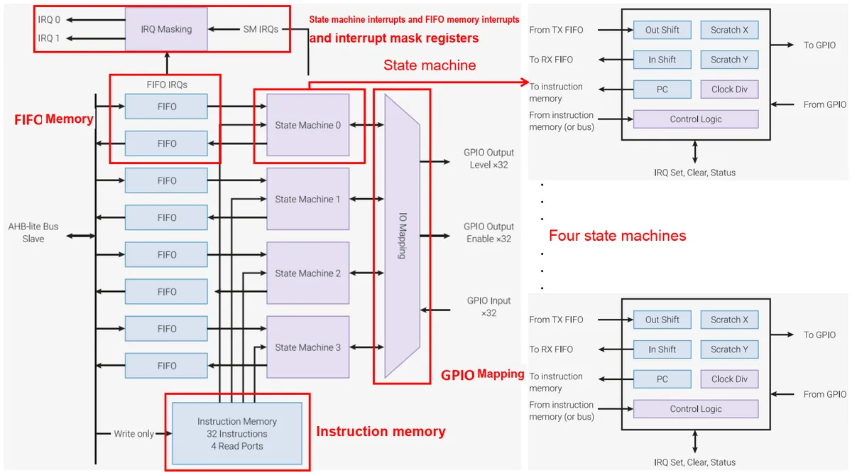
Simply put, the PIO peripheral consists of the following components:
- finite-state machine (State Machine): Each PIO contains 4 independent finite-state machines, which serve as the core execution hardware of the PIO and can be regarded as a lightweight dedicated processor, internally comprising:
- PC (Program Counter): Records the address of the instruction to be executed currently in the instruction memory, and controls the sequential execution of instructions;
- Clock Div (Clock Divider): Independently adjust the operating clock frequency of the finite-state machine to adapt to external I/O protocols with different rates;
- X/Y Erasable Data Register: Temporarily stores operation data and intermediate results;
- Out Shift (Output Shift Register): Shifts the data according to the specified bit width and sequence, then outputs it to the GPIO;
- In Shift (input shift register): Reads data from GPIO and shifts and temporarily stores it according to specified rules;
- The finite-state machine reads assembly instructions in the instruction memory via internal registers, and independently completes operations such as data read/write and GPIO control; meanwhile, it can access units including FIFO, DMA and GPIO, and generate interrupt signals for synchronization between finite-state machines as well as between PIO and the main CPU.
- Instruction Memory: a read-only memory unit with a capacity of 32 instructions, shared by 4 finite-state machines within the same PIO. The PIO-specific assembly instructions written by users will be loaded into this memory for each finite-state machine to read and execute independently;
- GPIO Mapping:
- The input/output signals of the finite-state machine can be mapped to the GPIO pins of the RP2040 (the hardware supports up to 32 GPIOs, while the RP2040 actually leads out 30 available GPIOs);
- All finite-state machines within the same PIO can independently and simultaneously access any GPIO pin, featuring flexible pin allocation capabilities.
- FIFO Memory: The Out Shift and In Shift shift registers of each finite-state machine are respectively connected to a set of "Transmit FIFO (Tx FIFO)" and "Receive FIFO (Rx FIFO)", whose core function is to realize the asynchronous decoupling between "data transmission and reception requests" and "actual execution operations":
- Transmission Scenario: The main CPU first writes the data to be output to the Tx FIFO; when the finite-state machine is ready, it fetches data from the Tx FIFO and outputs it to the GPIO via the Out Shift register.
- Reception Scenario: The finite-state machine temporarily stores the data read from the GPIO into the In Shift register, then writes it to the Rx FIFO; the main CPU can fetch the data from the Rx FIFO at an appropriate time.
- Interrupt and Interrupt Mask Registers: Used to manage the interrupt signals of the PIO:
- Interrupt sources: refer to the raw interrupt signals from components including FIFOs (e. g., FIFO full/empty status) and finite-state machines (e. g., instruction execution completion, specific operation trigger);
- Interrupt Mask Register: It configures the "enable/mask" state of the original interrupt signals, and only unmasked interrupts are sent to the RP2040 interrupt controller to trigger the response of the main CPU.
1.2 Programming Model of PIO and Working Principle of finite-state machine
The programming model of PIO peripherals shares commonalities with general-purpose processors: both implement functions by sequentially executing pre-written programs, can complete data interaction via the DMA/interrupt system, and realize state control by reading and writing control registers. However, unlike general-purpose processors, PIO is a hardware subsystem designed specifically for input and output scenarios, so it features strong timing determinism and high operation accuracy, and is deeply bound to fixed-function hardware such as GPIO and DMA.
The core of PIO's function implementation lies in the 4 independent finite-state machines it contains. Each finite-state machine features a highly integrated hardware structure (corresponding to the finite-state machine structure diagram), and its composition and working principle are as follows:
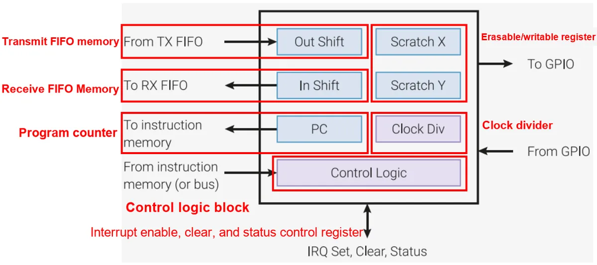
Including:
- Two 32-bit shift registers: corresponding to the "Out Shift (output shift register)" and "In Shift (input shift register)" in the structure diagram, both have a width of 32 bits, and support data shift operations in any direction and with any number of bits:
- Output Shift Register (
OSR): It receives data from the TX FIFO, shifts the data according to the rules configured by instructions, and then outputs the processed data to the GPIO; - Input Shift Register (
ISR): It reads data from GPIO, shifts and temporarily stores the data according to instruction rules, and then writes the data to the RX FIFO. The shift register is the core data path that connects the finite-state machine to the FIFO and GPIO.
- Output Shift Register (
- Two 32-bit erasable registers: corresponding to "Scratch X" and "Scratch Y" in the structure diagram, both with a width of 32 bits, are temporary data storage units for the finite-state machine during program execution, which can be analogized to "variables" in general programming and are used to temporarily store intermediate operation results, configuration parameters, etc. ;
- There are 4x32-bit bus FIFOs in each direction (TX/RX): corresponding to the "TX FIFO" and "RX FIFO" connected to the shift register in the structure diagram, which are the asynchronous data buffer units between the finite-state machine and external devices (CPU/DMA):
- Hardware Specifications: Each finite-state machine is default equipped with 4×32-bit FIFOs in both directions (4 pieces of 32-bit data depth for each of the TX FIFO and RX FIFO), which can be configured via the
SHIFTCTRL_FJOINoption to be combined into an 8×32-bit unidirectional FIFO, suitable for high-bandwidth scenarios such as DPI image display; - Data Interaction:
- TX FIFO: To be written with data to be output by the CPU or DMA for the finite-state machine to read from the Out Shift register;
- RX FIFO: Written by the finite-state machine with data from the In Shift register, for reading by the CPU or DMA.
- Rate Adaptation: The FIFO can generate DREQ request signals (the communication channel between the peripheral device and the DMA), based on which the DMA controller can perceive the storage status of the FIFO (such as full/non-empty/empty) and dynamically adjust the transmission rhythm to achieve rate matching.
- Hardware Specifications: Each finite-state machine is default equipped with 4×32-bit FIFOs in both directions (4 pieces of 32-bit data depth for each of the TX FIFO and RX FIFO), which can be configured via the
- Clock Divider (Clock Div): Corresponding to the "Clock Div" in the block diagram, it is a fractional divider with a 16-bit integer part and an 8-bit fractional part:
- The clock source is the system clock (e. g., 125MHz), which can divide the clock of the finite-state machine down to 1/65536 of the system clock (at 125MHz, the lowest divided clock is approximately 1908Hz);
- Its core function is to set an accurate operating rate for scenarios such as serial communication to ensure timing matching.
- Flexible GPIO Mapping: The finite-state machine supports 4 independent GPIO mapping modes (input mapping, output mapping, set mapping, and side-set mapping), and each finite-state machine can independently map its I/O operations to the GPIO pins of the RP2040 (supporting up to 30 available GPIOs) to achieve flexible pin assignment;
- DMA Interface: The finite-state machine connects to the on-chip DMA controller via the DMA interface, achieving a maximum interaction rate of "1 byte data transfer per system clock cycle" and supporting efficient transfer of large data volumes.
- Interrupt System: Corresponding to "IRQ Set, Clear, Status" in the block diagram, the PIO peripheral contains a total of 8 interrupt flag bits:
- Interrupt sources may come from the FIFO (e. g., FIFO full/empty) or the finite-state machine (e. g., instruction execution completed);
- Synchronization between finite-state machines, as well as between finite-state machines and the main CPU, can be realized by setting, clearing and querying the status of interrupt flags.
- Program Counter (PC): Corresponding to the "PC" module in the structure diagram, it serves as the instruction address pointer of the finite-state machine, which is used to point to the storage location of the PIO assembly instruction to be executed currently in the instruction memory and control the sequential execution flow of instructions;
- Control Logic Block: corresponding to the "Control Logic" module in the structure diagram, it serves as the control center of the finite-state machine. The system can configure other components (shift registers, clock dividers, etc.) of the finite-state machine and control their working states by reading from and writing to the registers within this module.
The PIO finite-state machine cannot directly execute assembly instructions written by humans. It is necessary to use the pioasm compiler (PIO Assembler) to compile the dedicated assembly instructions into corresponding machine codes, which are then loaded into the instruction memory of the PIO for execution by the finite-state machine. PIO provides 9 core pioasm assembly instructions, which cover all related basic operations such as jump, data transfer, GPIO control, and interrupt handling, and are the core syntax for implementing PIO functions. The specific instructions and their functions are as follows:
- JMP: Jump Instruction
- Function: Modify the program counter (PC) value of the finite-state machine to redirect the instruction execution flow to the specified memory address, supporting both unconditional jumps and conditional jumps (e. g., determining whether to jump based on conditions such as register values, pin states, FIFO states, etc.).
- Purpose: It implements logics such as branching, looping, and conditional execution of programs, serving as the fundamental instruction for building complex PIO programs.
- WAIT: Wait Instruction
- Function: Pauses the execution of the finite-state machine, and resumes executing subsequent instructions only after the preset waiting condition is satisfied. Waiting conditions are mainly divided into two categories:
- First, the GPIO pin status condition (e. g., waiting for a certain GPIO pin to be at high level / low level);
- Second, the clock cycle condition (e. g., waiting for a specified number of finite-state machine clock cycles to achieve precise delay).
- Applications: It enables timing synchronization with external devices (e. g., waiting for the ready signal from a sensor) and the generation of precise delay operations, ensuring the timing determinism of PIO operations.
- Function: Pauses the execution of the finite-state machine, and resumes executing subsequent instructions only after the preset waiting condition is satisfied. Waiting conditions are mainly divided into two categories:
- IN: Data Read Instruction
- Function: Read data from the specified source and move it into the input shift register (ISR). The data sources include GPIO pins (to read the level state of a single or multiple GPIOs), FIFO memory, internal registers of the finite-state machine, etc. , and the number of bits to be read can be specified.
- Purpose: It implements the core operation of reading data from external devices (via GPIO) or internal units, and serves as the primary method for PIO input data acquisition.
- OUT: Data Write Command
- Function: This module shifts out the data in the Output Shift Register (OSR) and writes it to a specified target, which includes GPIO pins (to control GPIO output levels), FIFO memory, finite-state machine internal registers, etc. , and supports specifying the number of bits to be written.
- Purpose: It implements the core operation of sending data to external devices (via GPIO) or internal units, and serves as the primary method for PIO to output data.
- PUSH: Data Push Instruction
- Function: This instruction pushes the complete data in the Input Shift Register (ISR) into the RX FIFO. After the push operation, users can choose to clear the ISR or retain the data, and can also configure whether to trigger an interrupt during the push process.
- Purpose: To transfer the data read by the finite-state machine from GPIO to the CPU or DMA (via the RX FIFO), thereby completing the external interaction of PIO input data.
- PULL: Data Pull Instruction
- Function: It pulls data from the TX FIFO and loads it into the Output Shift Register (OSR). After the pull operation, it is configurable whether to wait for new data when the TX FIFO is empty, and meanwhile, users can choose to clear the OSR or retain the original data in it.
- Purpose: To transfer the data written by the CPU or DMA (stored in the TX FIFO) to the finite-state machine, serving as the data source for PIO output.
- MOV: Data Movement Instruction
- Function: It moves or copies data between the internal registers of the finite-state machine. The supported operation objects include the Input Shift Register (ISR), Output Shift Register (OSR), X/Y erasable registers, GPIO pin configuration registers, etc. It can also implement simple operations such as data inversion and clearing.
- Purpose: It implements data processing inside the finite-state machine and data interaction between registers, which is equivalent to the variable assignment operation in general-purpose programming.
- IRQ: Interrupt Write or Clear Instruction
- Function: Operate the interrupt flag bits of PIO, including setting the interrupt flag (triggering an interrupt), clearing the interrupt flag (canceling an interrupt), and waiting for the interrupt flag (pausing execution until the interrupt is triggered); the interrupt flag bits to be operated can be specified (PIO has a total of 8 interrupt flag bits).
- Purpose: It implements synchronization between finite-state machines and event notification between finite-state machines and the main CPU, serving as the core operation instruction of the PIO interrupt mechanism.
- SET: Instruction for configuring mapped GPIO
- Function: Directly set the level state (high level / low level) of the specified GPIO pin, or configure the mapping mode (input / output / set / side setting) of the GPIO; the GPIO to be operated is the pin that has been mapped by the finite-state machine.
- Purpose: To achieve rapid level control over GPIO pins, which is suitable for simple output operations or GPIO mode configuration.
1.2.1 Control Flow of PIO
One of the core features of the PIO finite-state machine is the timing determinism of instruction execution, which is guaranteed by its fixed control flow mechanism. The instruction execution process of the finite-state machine follows strict clock cycle rules and supports flexible instruction fetch and execution modes, with the specific mechanisms as follows.
1.2.1.1 Instruction Execution Cycle of the finite-state machine
Each PIO finite-state machine completes the three stages of fetching, decoding and executing one pioasm assembly instruction within a single system clock cycle (these three stages are finished in one clock cycle without pipeline latency). Only special instructions (such as the WAIT instruction, which requires waiting for the condition to be met before proceeding) will break this rule and cause the finite-state machine to pause execution.
To enable cycle-accurate programming, PIO instructions also support the insertion of delay cycles: users can manually configure 1 to 31 additional clock cycles of delay before the next instruction is executed. This delay configuration is instruction-level, which can precisely match the timing requirements of external devices, such as the clock beats of serial communication and the response time of peripherals.
1.2.1.2 Working Mechanism of Program Counter (PC)
The program counter (PC) is a core component of the finite-state machine that controls the instruction execution sequence, and its operating logic is as follows:
- Default behavior: During the normal execution flow, the value of the PC will be automatically incremented by 1 at each clock cycle automatically incremented by 1, pointing to the address of the next instruction in the instruction memory to realize sequential instruction execution.
- Exception: When executing the
JMP(jump) instruction, the default auto-increment logic of the PC will be overridden.The JMPinstruction explicitly specifies the next value of the PC (i. e., the position of the next instruction to be executed in the instruction memory), thereby implementing control flow logic such as program branching, looping, and conditional jumps.
1.2.1.3 Extended Acquisition Sources of Instructions
By default, the instructions executed by the finite-state machine are fetched from the PIO's instruction memory. However, to enhance flexibility, the PIO also supports fetching and executing instructions from the following special regions, which enable advanced operations such as the "instruction and data stream fusion":
- Special Configuration Register (SMx INSTR)
- Mechanism: When writing an instruction to the
SMx INSTRregister corresponding to the finite-state machine (where x is the finite-state machine number, ranging from 0 to 3), this instruction will immediately interrupt the current instruction execution flow of the finite-state machine and be executed with priority. - Example: Writing a
SMx INSTRwith aJMPinstruction will cause the finite-state machine to immediately abandon the currently executing instruction sequence and start executing new instructions from the address specified byJMP. - Features: It has the highest execution priority and is applicable to emergency instruction intervention or immediate retargeting of the finite-state machine.
- Mechanism: When writing an instruction to the
- MOV EXEC instruction
- Mechanism: Through the
MOV EXECinstruction, the finite-state machine can read and execute instructions from internal registers (instructions are stored in registers in the form of data). - Execution Timing:
The MOV EXECinstruction itself requires 1 clock cycle to execute, and then takes another 1 clock cycle to execute the target instruction read from the register.
- Mechanism: Through the
- OUT EXEC Instruction
- Mechanism: Through the
OUT EXECinstruction, the finite-state machine can read and execute instructions from the Output Shift Register (OSR) — the instructions are embedded as data in the data stream of the shift register. - Execution timing: consistent with
MOV EXEC,the OUT EXECinstruction itself occupies 1 clock cycle, and the target instruction is executed subsequently.
- Mechanism: Through the
1.2.2 Introduction to Internal Registers of the PIO finite-state machine
Each finite-state machine has several internal registers, which are used to store input or output data as well as temporary data such as loop variables.
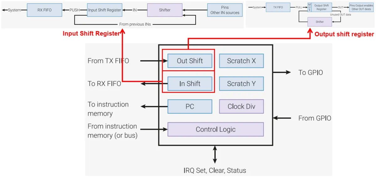
Data flow between multiple registers is realized via the control logic of a finite-state machine: for example the IN instruction shifts GPIO data into the In Shift, after which the data can be copied to the Scratch X temporary storage via the MOV instruction; once processing is complete, the data is written to the Out Shift via the MOV instruction, and finally output to GPIO via the OUT instruction. No intervention from the main CPU is required throughout the entire process, which ensures the independence, high efficiency and timing accuracy of the PIO.
1.2.2.1 Output Shift Register OSR
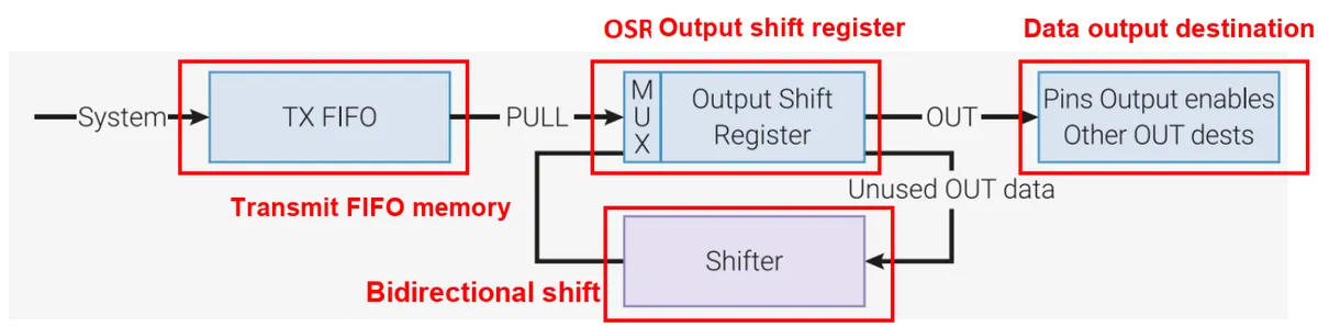
Corresponds to the Output Shift Register module in the output data flow diagram, which is the temporary storage and processing unit for finite-state machine output data. Its hardware connection relationship is: TX FIFO (transmit FIFO memory) → OSR → bidirectional shifter (Shifter) → output destination (such as Pins Output enables).
It is responsible for implementing data storage and shift output between the TX FIFO and GPIO pins (or other output targets such as erasable registers), supporting a maximum of 32 bits of Data Parallelism output in a single operation; unused output data will be recovered by the bidirectional shifter to avoid data loss:
- Data Loading: Pull data from the TX FIFO via the
PULLinstruction and store it in the OSR; when the OSR is empty, data will also be automatically loaded from the TX FIFO. - Data Output: The
OUTinstruction outputs the data in the OSR to the specified target, supporting output of 1 to 32 bits of data in a single operation; upon completion of output, the OSR will be fully filled with 0s. - Auto-loading (autopull): This function can be enabled by configuring the control logic block. When the output shift counter reaches the set threshold, the finite-state machine will automatically execute
PULLinstruction to load data from the TX FIFO. This function eliminates the need to manually execute thePULLinstruction, which saves instruction cycles and improves data throughput.
1.2.2.2 Input Shift Register (ISR)

Corresponding to the Input Shift Register module in the input data flow diagram, it is the temporary storage and processing unit for finite-state machine input data, and its hardware connection relationship is: input source (Pins, etc.) → bidirectional shifter (Shifter) → ISR → RX FIFO (receive FIFO memory).
It is responsible for implementing data storage and shift input between GPIO pins (or other input sources) and the RX FIFO, supporting up to 32 bits of Data Parallelism input in a single operation; unprocessed input data will be temporarily stored by the bidirectional shifter to ensure data continuity:
- Data input: The
INinstruction is used to shift data from the bidirectional shifter into the ISR, with a single input supporting 1 to 32 bits of data. - Data Push: The
PUSHinstruction writes the data in the ISR to the RX FIFO for reading by the CPU or DMA. - Auto-push (
autopush): This function can be enabled by configuring the control logic block. When the input shift counter reaches the set threshold, the finite-state machine will automatically execute thePUSHinstruction to push the data in the ISR to the RX FIFO.
1.2.2.3 Shift Counter Shifter
It is a pair of hardware counters (input shift counter, output shift counter) built into the finite-state machine, which are used to track the number of input data bits of the ISR and the number of output data bits of the OSR, with a counting range of 0 to 32 (inclusive of the boundary values):
- Each time an
INinstruction is executed, the input shift counter increments by the corresponding number of data bits; - Each time an
OUTinstruction is executed, the output shift counter increments by the corresponding number of data bits; - The maximum value of the shift count is 32 (consistent with the width of the shift register).
By configuring the counter via the control logic block, the following operations can be automatically triggered when the counter reaches the specified threshold:
- When the output shift counter reaches the threshold, the system will automatically execute
OUTinstruction to output the OSR data to the target. - When the input shift counter reaches the threshold, the
INinstruction is automatically executed to move the data of the bidirectional shifter into the ISR; - Automatic execution based on counter conditions
PUSH/PULL:- Automatic
PULL(between OSR and TX FIFO): The output shift counter is cleared upon execution; - Automatic
PUSH(between ISR and RX FIFO): The input shift counter is cleared after execution.
- Automatic
When resetting (or enabling CTRL_SM_RESTART): the input shift counter is cleared (indicating no input data in the ISR), and the output shift counter is set to 32 (indicating no output data in the OSR):
MOV OSR, . ..(theMOVinstruction written to OSR): clears the output shift counter;MOV ISR, . ..(theMOVinstruction written to ISR): input shift counter reset to zero;OUT ISR, count: Set the input shift counter tocount.
1.2.2.4 Erasable Register
Each finite-state machine contains two independent 32-bit general-purpose registers (named X and Y) with no fixed function binding, which serve as the "temporary variable carriers" for PIO programs:
- As the source/target address for data operations: it supports data transmission for instructions including
IN/OUT/SET/MOV, etc. - Data sources as branch conditions: support conditional judgment of instructions such as
JMP.
The following is a sample assembly program for operating the erasable and writable registers. In the code below, we generate a sequence of multi-segment long high-level pulses and short low-level pulses to produce the timing signals required for the WS2812, so as to control the WS2812 LED strip:
.program ws2812_led

public entry_point:
    pull ; get the current state of the input pins
    set x, 23 ; initialize register x to 23, used to loop over 24 bits

bitloop:
    set pins, 1 ; drive the output pin high
    out y, 1 [5] ; shift 1 bit out of the output shift register and write it into register y
    jmp !y skip ; check the value of register y to decide whether the extra delay is needed; if y is 0, jump to skip
    nop [5] ; delay 5 clock cycles

skip:
    set pins, 0 [5] ; drive the output pin low
    jmp x-- bitloop ; if register x is non-zero, decrement it and decide from its value whether to keep looping; if non-zero, jump to bitloop
    jmp entry_point ; after the loop ends, jump back to the program entry point
wherein the public entry_point: statement is used to define the program entry point, and the bitloop: statement label defines the start position of the bit loop:
- The function of register X: as a loop counter, its initial value 23 corresponds to 24-bit data (the color data length of a single WS2812 LED bead), and it is decremented via
x--in each loop to realize the control of 24-bit output; - The function of register Y: as a temporary variable, it stores the 1-bit data shifted out from the OSR, and is used for
JMPinstruction condition judgment (to distinguish different delays corresponding to 0 and 1, so as to match the timing requirements of WS2812);
The execution process of the code is as follows:
- The program first acquires the current state of the input pin, and pulls the LED bead data from the TX FIFO;
- Then enter the bit loop, which is controlled by X to run 24 times, and each loop outputs one bit value (0 or 1) to the LED strip;
- Loop 24 times to complete the output of 24 bits, distinguish the bit values via Y and generate the corresponding timing sequence;
- Finally, it jumps back to the program entry point and repeats the above process.
1.2.3 Wait State of the PIO finite-state machine
The instruction execution of the PIO finite-state machine generally follows the rule of being completed in a single cycle, but under specific conditions, the finite-state machine will enter a waiting state (pausing instruction execution). The waiting state is a hardware behavior designed by PIO to adapt to external timing and data interaction rhythm, and its trigger conditions, hardware performance and special processing mechanism are as follows.
1.2.3.1 Trigger Conditions for a finite-state machine to Enter the Waiting State
The core reason why the finite-state machine pauses execution is that the execution conditions of the current instruction are not met, which can be specifically divided into the following five types of scenarios:
- Delay condition of WAIT instruction not met: When executing
WAITdelay instruction, if the preset delay time has not elapsed (or the GPIO pin status or interrupt flag does not meet the waiting condition), the finite-state machine will suspend execution until the condition is satisfied; - Abnormal FIFO status of blocking PULL/PUSH instructions:
- When executing the blocking mode
PULLinstruction, if the TX FIFO is empty (no data available to pull), the finite-state machine will pause until the CPU/DMA writes data to the TX FIFO; - When executing the blocking mode
PUSHinstruction, if the RX FIFO is full (no space to store data), the finite-state machine will pause until the CPU/DMA reads data from the RX FIFO; - The PULL/PUSH instructions of PIO support both blocking and non-blocking modes. The behavior described above corresponds to the blocking mode, and no waiting will be triggered in the non-blocking mode.
- When executing the blocking mode
- The interrupt flag bit of the IRQ WAIT instruction is not cleared: When executing
the IRQ WAITinstruction, if the IRQ interrupt flag bit set in the instruction is not cleared (the interrupt is not released), the finite-state machine will suspend execution until the interrupt flag bit is cleared; - OUT instruction trigger wait under autopull: After the autopull function is enabled, when the OSR reaches the count threshold of the shift counter, the finite-state machine will trigger an automatic
PULLoperation; if the TX FIFO is empty (no data available for loading) at this point, the finite-state machine will pause and wait for the CPU/DMA to write data to the TX FIFO. - IN instruction trigger wait under autopush: After the autopush function is enabled, when the ISR reaches the count threshold of the shift counter, the finite-state machine will trigger an automatic
PUSHoperation; if the RX FIFO is full (no space for storage) at this time, the finite-state machine will pause and wait for the CPU/DMA to read data from the RX FIFO.
1.2.3.2 Program Counter (PC) Behavior in Wait State
When the finite-state machine is in the waiting state, the value of the program counter (PC) remains unchanged, and no increment or jump operation will be performed. The finite-state machine rechecks the waiting condition at every clock cycle: if the condition is still not resolved, it continues to pause; if the condition is resolved, it immediately resumes executing the current instruction, and then restores the normal PC increment or instruction jump logic.
1.2.3.3 Side-set Operations and Side-set Mapping
Side-set is a combination of a special GPIO mapping method and instruction-level operation for the PIO finite-state machine, which is not only one of the four GPIO mapping modes but also a core synchronization tool for handling wait states.
1.2.3.3.1 Side Set Mapping (Hardware Configuration Level)
Side-set mapping is one of the four GPIO mapping modes of PIO, whose core lies in deeply binding specific GPIOs with the instruction execution flow of the finite-state machine, serving as the hardware foundation for side-set operations.
- Core Definition: Pre-configure the "side-set pins"(up to 5 GPIOs) for the finite-state machine, and specify the active level (high/low) of the side-set signal; when the finite-state machine executes any instruction, it can output the preset side-set signal synchronously to control the level of the corresponding pins;
- Key Features: Side-set operations are completed in the same cycle as instruction execution, with no additional clock overhead, enabling extremely precise timing control.
| Mapping Method | Control Timing | Main Purpose |
| Input Mapping | Actively read GPIO level | Receive input signals from external devices |
| Output Mapping | Controlled by the OUT instruction | Send data to external devices |
| Set Mapping | Controlled by the SET instruction | Control GPIO levels individually (set high / low) |
| Side-set Mapping | Control accompanies execution of any instruction | Synchronized timing of instructions and GPIO control (e.g., pin control for communication protocols) |
1.2.3.3.2 Side Set Operation
Side-set operation is an instruction-level behavior based on side-set mapping, and it is the actual implementation approach of the side-set function:
- Number of side-set pins: Configured via the
PIO_SM_CONFIGside_set_bitsfield (1~5 bits, corresponding to 1~5 side-set pins); - Driving mode: Configure the active level (high/low) and driving type (push-pull/open-drain) of the side set pins via the control register.
1.2.3.3.3 Special Functions of Side-set Operations
The wait state of a finite-state machine pauses most instruction-related operations, but Side-set operations are not affected by the wait state:
- Side-set operations are bound to instructions: regardless of whether an instruction enters a waiting state, the side-set operation will be executed in the first clock cycle of the instruction to which it belongs;
- The core value of this feature is that even when the finite-state machine is paused, the level of the specified GPIO pin (such as the control pin of the Communication Protocol) can still be controlled via side-set operations, ensuring that the timing synchronization of external devices will not be interrupted.
The core value of side-set mapping and operations lies in realizing latency-free binding between instructions and GPIO control, which can maintain the timing stability of external devices especially in the wait state, with typical scenarios including:
- Communication Protocol Synchronization: In SPI communication, configure the chip select (CS) pin as a side-set pin, and pull CS low synchronously when
OUTtransmitting data; even if thepullinstruction waits due to an empty TX FIFO, CS remains asserted to prevent communication abnormalities of the slave device; - High-Speed Timing Generation: In the DPI display driver, set the horizontal synchronization (HSYNC) pin as a side-set pin, and execute it synchronously with the data output instruction to ensure precise timing matching between the synchronization signal and the data;
- State retention in the waiting state: When the finite-state machine is waiting due to an interrupt, it outputs a "busy" signal through the side-set pins to prevent external devices from making repeated requests.
1.2.4 GPIO Pin Mapping of PIO
The GPIO pin mapping of PIO is a physical connection configuration mechanism for its interaction with external hardware, which defines the rules for the finite-state machine to control and read GPIO pins, serves as the foundation for PIO to implement external interface functions, and its core logic is as follows:
- GPIO control capability of PIO: PIO supports controlling the output level and direction of up to 32 GPIOs, as well as reading input levels; in the RP2040 hardware, the actual number of user GPIOs that can be mapped is 30.
- GPIO operation limit per clock cycle: Within a single system clock cycle, each finite-state machine can perform a maximum of 2 GPIO operations, and the supported operation combinations include:
- Instruction-based operations: Modify the level/direction of GPIO via
OUT/SETinstructions, or read the GPIO level viaINinstructions; - Side-set operations: Modify the GPIO level/direction via side-set operations;
- Each cycle can perform "zero, one (either an instruction or a side set), or two (an instruction + a side set)" operation (s).
- Instruction-based operations: Modify the level/direction of GPIO via
The operation range of the finite-state machine for GPIO is determined by its PINCTRL register:
- Each operation (
OUT/SET/IN/side-set) can specify a consecutive block of 4 GPIOs, and the starting pin number of this GPIO block is configured via thePINCTRLregister; - The GPIO coverage of a single operation can be extended to any number of GPIOs within the PIO block (30 user GPIOs in the RP2040);
- The GPIO ranges for different operations (such as
OUTand side-set) can overlap, allowing the same set of GPIOs to be controlled by multiple operations.
When multiple operations write to the same GPIO within the same clock cycle, the PIO applies the operation results according to the following priority rules:
- finite-state machine priority: starting from the finite-state machine with the largest number, apply its write operations in sequence;
- Operation priority for the same finite-state machine: When the same finite-state machine simultaneously performs
SET/OUTand side-set operations on the same GPIO, the result of the side-set operation takes effect first; - Retention rule without write operation: If no finite-state machine performs a write operation on a certain GPIO, the level/direction of this GPIO will maintain the state of the previous cycle.
In practical use, the output operations of each finite-state machine are usually mapped to different GPIO groups, so that a single PIO block can drive multiple independent external interfaces simultaneously (for example, one finite-state machine maps GPIO0~3 to implement UART, and another finite-state machine maps GPIO4~7 to implement SPI), thus maximizing the utilization of PIO hardware resources.
1.2.5 IRQ Interrupt Flag Bit of PIO
The IRQ interrupt mechanism of PIO is the core approach for synchronization between finite-state machines and communication between finite-state machines and the main CPU, which consists primarily of the "IRQ interrupt flag bits" and "interrupt enable registers (IRQ0_INTE, IRQ1_INTE)".
The IRQ interrupt flag bits of PIO are status bits that can be set / cleared by a finite-state machine or the system, and are used to indicate the occurrence of specific events. There are 12 flag bits in total (corresponding to the register bit definitions), which are divided into three categories:
- SMx flag bits (x= 0~3): system-level interrupt flag bits, which are actively set by a finite-state machine or the system for synchronization between finite-state machines or triggering interrupts to the main CPU;
- SMx_TXNFULL flag (x= 0~3): This is the TX FIFO non-full flag of finite-state machine x, which is triggered when there is free space in the TX FIFO;
- SMx_RXNEMPTY flag bits (x= 0~3): These are the RX FIFO non-empty flag bits for finite-state machine x, which are triggered when there is data in the RX FIFO.
The status of these flag bits can be read through the PIO's INTR (interrupt status register) and INTS (interrupt raw status register).
IRQ0_INTE and IRQ1_INTE are interrupt enable configuration registers of the PIO, used to control which IRQ flag bits can trigger interrupt requests (corresponding to the irq0 and irq1 interrupt lines of the RP2040 respectively); the two have completely identical structures, and only differ in the interrupt lines they correspond to.
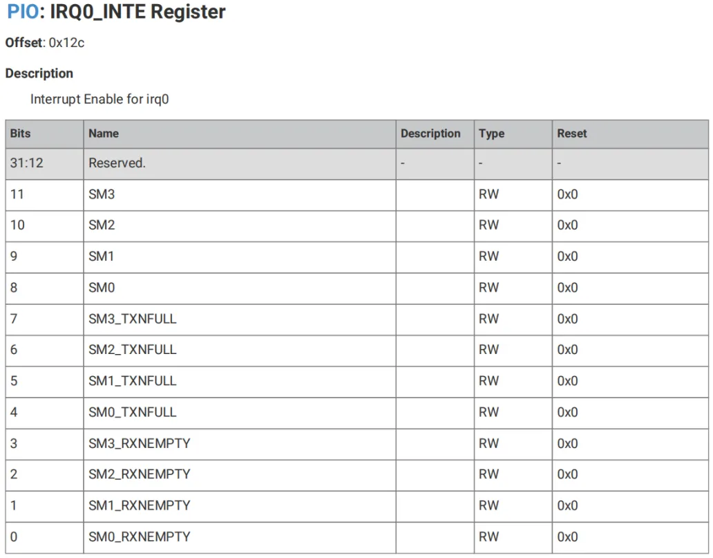
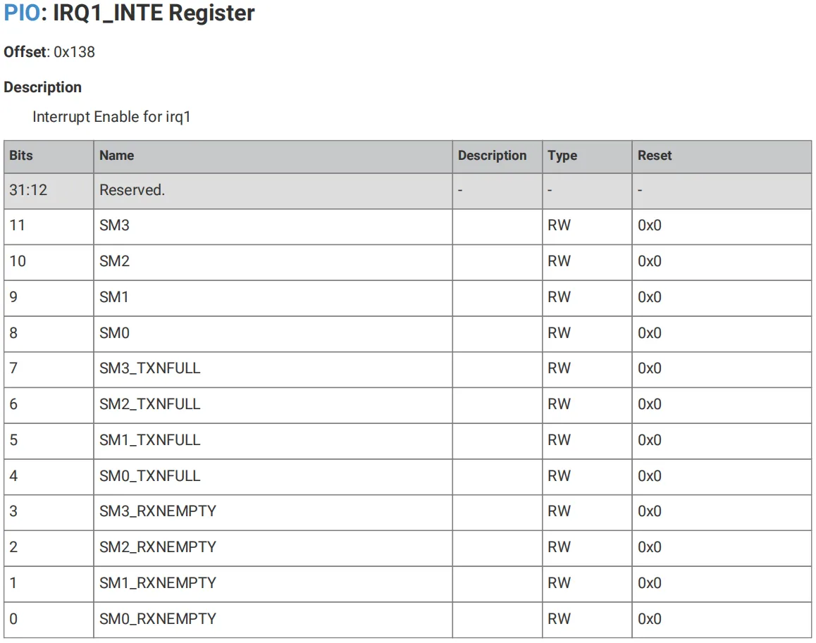
IRQ0_INTE IRQ1_INTE The low 12 bits of the register (Bit0~ Bit11) correspond to various IRQ interrupt flags of PIO (including 4 system-level SMx flags, 4 TX FIFO non-full flags, and 4 RX FIFO non-empty flags), and the high bits (Bit12~ Bit31) are reserved bits reserved by the chip (no function, no need to worry):
- Enable Configuration: Write
1to the corresponding bit of the register to enable this flag bit to trigger the corresponding irq (irq0 or irq1); writing0will mask the interrupt request of this flag bit; - Reset State: The reset value of all bits in the register is
0x0, meaning that after PIO initialization, all interrupts corresponding to the IRQ flag bits are in a masked state by default; - Interrupt Triggering: When a flag bit is set and the corresponding enable bit is
1, the PIO will send an irq0/irq1 request to the interrupt controller of the RP2040, triggering the interrupt handling process of the main CPU.
IRQ flags are mainly used for the following purposes:
- Event handling within a finite-state machine program: A finite-state machine can implement conditional execution logic within the program via
IRQinstructions (set/clear flag bits) andWAITinstructions (wait for flag bit states); - Synchronization between finite-state machines: Multiple finite-state machines can synchronize their execution timings by sharing IRQ flags (e. g., finite-state machine A sets a flag after completing an operation, and finite-state machine B starts after waiting for this flag);
- Communication with the main CPU: By enabling the interrupt of the flag bit, the finite-state machine can notify the main CPU of events (such as TX FIFO being empty and RX FIFO having data) to trigger the subsequent processing of the CPU.
1.2.6 Synchronization of PIO finite-state machine
The 4 finite-state machines of the PIO feature parallel execution and independent operation, and support precise clock-cycle-level synchronization via IRQ interrupt flags, which is the core capability that enables the PIO to handle multiple interfaces or complex timing tasks simultaneously. The 4 finite-state machines of the PIO share the instruction memory but operate in full parallel at the execution level. Multiple finite-state machines can read and execute the same instruction (or different instructions) from the instruction memory within the same system clock cycle without waiting for each other:
- Multiple finite-state machines execute the same program:
- Scenario: It is required to drive multiple identical external devices at the same time (such as multiple sets of WS2812 LED strips, multiple identical SPI slave devices).
- Advantages: Only one PIO assembly program needs to be written, and multiple finite-state machines execute in parallel, which reduces program development workload and ensures the consistency of device control logic.
- Multiple finite-state machines execute different programs:
- Scenario: It is required to implement multiple distinct Communication Protocols or I/O functions simultaneously (e. g., one finite-state machine for UART transmission, one for SPI reception, and one for GPIO pulse detection).
- Advantages: A single PIO block can simultaneously process multiple independent I/O tasks, maximizing the utilization of PIO hardware resources and avoiding occupying the computing power of the main CPU.
- Multiple finite-state machines execute different units of the same interface in a divided manner:
- Scenario: Functional decomposition of complex interfaces, where different timing tasks are assigned to respective finite-state machines.
- Example:
- UART communication: one finite-state machine is responsible for the TX (transmit) terminal, and the other is responsible for the RX (receive) terminal;
- DPI image shows: one finite-state machine is responsible for clock / horizontal synchronization signal generation, and the other is responsible for pixel data output.
- Advantages: It splits complex timing sequences into simple subtasks, reduces the difficulty of writing a single program, and ensures the timing synchronization of each unit of the interface at the same time.
Data cannot be directly communicated between the finite-state machines of PIO, but precise synchronization can be achieved via the IRQ interrupt flag, with the synchronization accuracy reaching a single clock cycle. The specific implementation method is as follows:
- The core tool for synchronization: The 8 IRQ interrupt flags of PIO (system-level SMx flags, FIFO status flags) serve as the "synchronization signal carriers" between finite-state machines, and all finite-state machines can read, set, and clear these flags.
- Synchronized instruction support:
IRQinstruction: Any finite-state machine can use this instruction to set or clear any IRQ flag bit (for example, after finite-state machine 0 completes data transmission, the SM0 flag bit is set);WAIT IRQInstruction: The finite-state machine can use this instruction to wait for a certain IRQ flag bit to be set or cleared (for example, finite-state machine 1 starts data reception after waiting for the SM0 flag to be set).
- Synchronous implementation logic: Through the process of "finite-state machine A sets/clears the flag bit → finite-state machine B waits for the flag bit state change before executing operations", the execution rhythm alignment of multiple finite-state machines is achieved, attaining the synchronization effect at the clock cycle level.
1.3 PIO Assembly Syntax
The PIO assembler (pioasm) is a tool that converts PIO assembly source files into executable machine code, and the assembly code it outputs can be integrated into applications for the RP2040 (including C/C++ programs built with the SDK and MicroPython programs); one of the core components of the PIO assembly syntax is identifiers, which are used to define program structures, constants, configuration parameters, etc. , and serve as the foundation for writing PIO assembly programs.
1.3.1 Identifiers
An identifier is a special instruction in PIO assembly used to define constants, program names, memory offsets, and configuration parameters. It is unrelated to register operations and only serves to control the structure and compile behavior of the program. The following are the syntax, functions, and usage rules for each identifier:
| Directive | Syntax | Core Meaning and Usage | Constraints / Notes |
| .define | .define (PUBLIC) <symbol> <value> | Defines integer symbol <symbol> with value <value>: 1. Global definition: appears before the first .program and applies to all programs; 2. Local definition: inside a .program and applies only to the current program; 3. With PUBLIC: the symbol is output to the assembled result for use by user code. | <symbol> must follow naming rules (letters, digits, underscores, not starting with a digit); <value> must be an integer. |
| .program | .program <name> | Starts a new PIO program named <name>; the program ends at the next .program or the end of the source file. All PIO instructions must be written inside a .program block. | <name> follows the same naming rules as above; PIO instructions cannot appear outside a .program. |
| .origin | .origin <offset> | Specifies the offset address <offset> (integer) in PIO instruction memory at which the program is loaded; commonly used to load the program at offset 0 (to suit the absolute addresses of JMP instructions). | Valid only inside a .program; in most cases it does not need to be specified manually, as the system allocates it automatically. |
| .side_set | .side_set <count> (opt) (pindirs) | Parameters for configuring side-set: 1. <count>: number of side-set data bits (1~5); 2. opt: optional, makes the side-set parameter optional for instructions (uses 1 extra delay bit); 3. pindirs: optional, makes side-set act on the GPIO direction register (PINDIR) rather than the level register (PIN). | Can only appear before the first instruction of a .program; it is a global configuration for side-set operations. |
| .wrap_target | .wrap_target (placed before an instruction) | Marks the start position of program wrap-around: when the program wraps, execution continues from the instruction after this directive. | Valid only inside a .program; can be used only once per program; If not specified, wraps to the beginning of the program. |
| .wrap | .wrap (placed after an instruction) | Marks the trigger position of program wrap-around: after the instruction before this directive is executed, the program wraps to the position marked by .wrap_target. | Valid only inside a .program; Can be used only once per program; If not specified, the wrap point is after the last instruction of the program. |
| .lang_opt | .lang_opt <lang> <name> <option> | Specifies language-generator-specific options for the program (e.g., parameters for the C generator, configuration for the MicroPython generator). | Valid only inside a .program; <lang> is the language type (e.g., c, python). |
| .word | .word <value> | Stores the 16-bit integer <value> as an instruction in PIO instruction memory (used to manually insert machine code). | Valid only inside a .program; <value> is a 16-bit integer (in the machine-code format of PIO instructions). |
1.3.2 Data Types
The data types in PIO assembly are primarily used to define integer constants and specify the target addresses for branch conditions, and they support multiple numerical representation formats and custom symbols. The specific types and their descriptions are as follows:
Data Type | Description | Example | Typical Use |
| Decimal integer value, supporting both positive and negative numbers |
| Define the delay period and the initial value of the counter |
| Hexadecimal value starting with |
| Indicates hardware register addresses and bitmasks |
| A binary value starting with |
| Indicates GPIO pin combinations and bit operation values |
| Symbols (constants) defined by | First | Improve code readability to facilitate unified modification |
| The labels in the program correspond to the offsets of the instructions in memory |
| Branch target address of the JMP instruction |
| Evaluable expression with parentheses (parentheses are mandatory) |
| Complex Numerical Calculation |
1.3.3 Expressions
Expressions are used to perform arithmetic and bitwise operations in combination with pioasm values; the operation result is an integer and can be used as the value of a data type. The specifically supported operations and their descriptions are as follows:
Expression Syntax | Description | Example | Operation Result |
| The sum (addition) of two expressions |
| 8, 0x5 |
| The difference (subtraction) between two expressions |
| 6, 4 |
| The product (multiplication) of two expressions |
| 24, 6 |
| The quotient of two expressions (integer division, with the fractional part discarded) |
| 3, 3 |
| Negative value (negation) of an expression |
| -5, -5 |
| Bitwise NOT of an expression (note the use of two colons) |
| 0b0110 |
| Any valid value (as the basis of the expression) |
| Corresponding value |
1.3.4 Notes
Comments are used to add descriptive text to the code and will not be compiled by the assembler. PIO assembly supports three comment formats to meet different commenting needs:
| Comment Style | Syntax | Description | Example |
| Line comment (//) | // comment text | Everything from // to the end of the line is a comment; compatible with C/C++ style | set x, 23 // initialize loop counter |
| Line comment (;) | ; comment text | Everything from ; to the end of the line is a comment; compatible with traditional assembly style | pull ; Pull data from the TX FIFO |
| Block comment (/* */) | /* multi-line comment text */ | A comment spanning multiple lines, starting with /* and ending with */; compatible with C style | /* This is a multi-line comment<br>used to describe the timing logic of WS2812 */ |
1.3.5 Tags
A label is essentially an automatic. define, with its value set to the offset of the current program instruction.
The format of the tag is as follows:<symbol>: or PUBLIC <symbol>:.
The tag must start at the beginning of a line.
Labels defined as PUBLIC can be accessed from user code in the same manner as PUBLIC. define directives.
.program example
PUBLIC entry_point: ; public label, accessible to external code
    set x, 10       ; instruction offset 0
loop:               ; normal label, corresponds to offset 1
    jmp x-- loop    ; jump to the loop label
    jmp entry_point ; jump to the entry_point label
In the above example, entry_point has a value of 0 (corresponding to the first instruction), and loop has a value of 1 (corresponding to the second instruction).
1.3.6 Instructions
All PIO assembly instructions follow a unified syntax format, support side-set and delay configuration, and serve as the standard specification for PIO instruction programming:
<instruction> (side <side_set_value>) ([<delay_value>])The meanings of the respective parameters are as follows:
| Parameter | Meaning and Constraints |
| <instruction> | PIO assembly instruction and its operands (such as pull, out y, 1, jmp loop); the core part of the instruction. |
| side <side_set_value> | Optional / required parameter: 1. Prerequisite: the number of side-set bits must first be configured with .side_set, otherwise this parameter is invalid; 2. Optionality: optional if .side_set specifies opt, required if not; 3. Value: the number of bits of side_set_value must match the number of bits configured by .side_set. |
| [<delay_value>] | Optional parameters: 1. Value range: 0~31 by default (5 bits); if side-set is enabled, the number of bits is reduced (the bits used by side-set are deducted from the delay bits); 2. Function: number of clock cycles to delay after the instruction completes; if not specified, there is no delay. |
Examples are as follows:
.program example
.side_set 1 ; configure 1-bit side-set (required parameter)
    pull side 0       ; side-set value 0, no delay
    out y, 1 side 1 [5] ; side-set value 1, delay 5 cycles
    jmp loop [3]      ; no side-set (error, because .side_set does not specify opt, so side-set is required)
    jmp loop side 0 [2] ; side-set value 0, delay 2 cycles
loop:
    nop side 1 [0]    ; no operation, side-set value 1, no delay
1.3.7 Pseudo-instructions
Pseudo-instructions are syntactic sugar provided by pioasm. They are not natively supported by PIO hardware, but are converted by the assembler into equivalent native instructions to simplify programming. Currently, pioasm provides only one pseudo-instruction:
nopPseudo-instruction: The assembler will convertnopinto a native instructionmov y, y(assigns the value of the Y register to itself, with no side effects).
It can be applied in the following scenarios:
- Side set coordination operation: When no core instruction needs to be executed,
nopis used to trigger the side set to control GPIO; - Add delay: Executing the
nopinstruction takes up 1 clock cycle, which can be used to fine-tune the timing; - Placeholder: Fill the instruction memory and adjust the program offset.
.program example
.side_set 1
    nop side 1 [5] ; no operation, side-set value 1, delay 5 cycles (6 cycles in total: 1 instruction cycle + 5 delay cycles)
    nop [3]        ; no operation, no side-set (error if .side_set does not specify opt), delay 3 cycles
1.4 PIO Instruction Set
The PIO instruction set contains a total of 9 instructions, each of which is 16 bits in length and is divided into 3 fixed fields according to their functions (corresponding to the instruction encoding table):
- Instruction Encoding Field (Bit15~13): 3 bits, used to distinguish different instructions (e. g., JMP corresponds to
000, WAIT corresponds to001); - Side Set / Delay Period (Bit12~8): 5 bits, used to store the side set operation value and delay cycle count; the specific allocation rule depends on the finite-state machine's
SIDESET_COUNTconfiguration (up to 5 bits, of whichSIDESET_COUNTbits are allocated for side set, and the remaining bits are used for delay); - Instruction Parameter Field (Bit 7 to 0): 8 bits, used to store specific parameters of the instruction such as conditions, addresses, source/destination, and bit length.
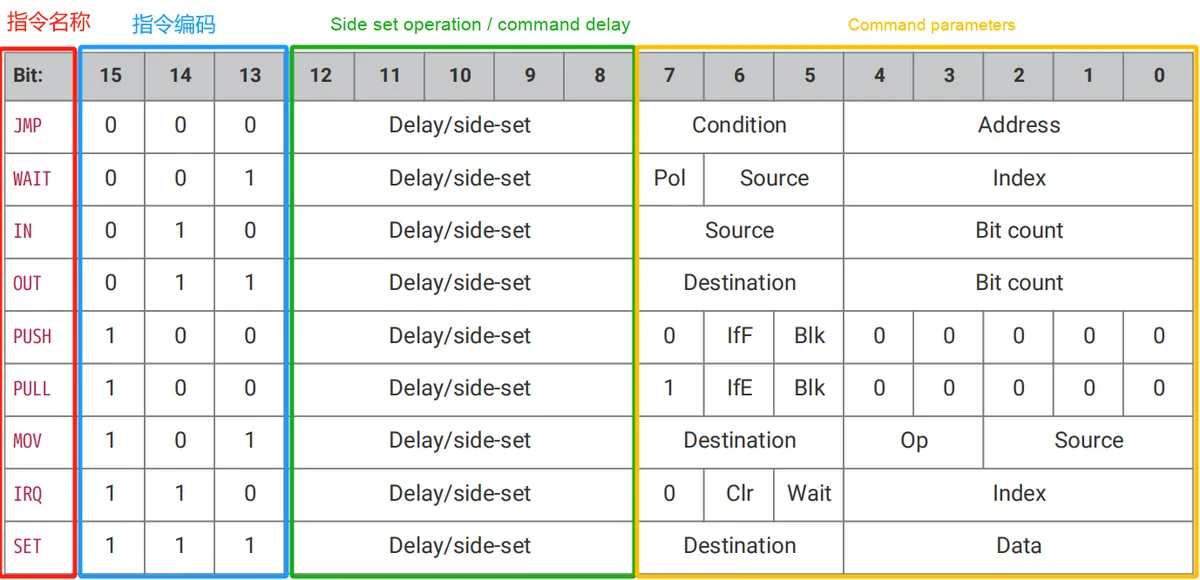
All PIO instructions have an execution time of one clock cycle.
The meaning of the 5-bit Delay/side-set field depends on the SIDESET_COUNT configuration of the finite-state machine:
- The maximum of 5 LSB bits (with a bit length of 5 - SIDESET_COUNT) represent the number of Delay cycles inserted between the current instruction and the next instruction.
- Up to 5 MSB bits (with a bit length of SIDESET_COUNT) are used for side-set operations, which can set certain GPIO pins to a specific constant while the instruction is being executed
Here, the delay operation can be applied when we require precise timing and/or signal synchronization, while the side-set operation allows us to additionally set pins while executing an instruction. This is very useful for control signals such as clocks and enables: the side-set operation is used to control pins, whereas instructions like OUT and MOV are used to process data.
The specific meaning of each instruction is introduced as follows.
1.4.1 JMP Jump Instruction
The JMP jump instruction is used to determine whether to execute an instruction jump according to a condition, so as to change the sequential execution flow of the current program.

Determine whether to modify the Program Counter (PC) according to the Condition: if the condition is true, set the PC to the instruction address corresponding to Address; otherwise, keep the PC incrementing automatically. Regardless of whether the condition is satisfied, the instruction consumes 1 clock cycle, and the delay is executed after the condition evaluation.
When the JMP instruction is executed, it always consumes one clock cycle regardless of whether the Condition is true. The Delay occurs after the Condition is evaluated and the program counter is updated.
The parameters are defined as follows:
Condition: Condition is a 3-bit binary value (corresponding to 000 to 111) that determines "when the jump occurs". You can think of it as a "switch for whether to jump", and each switch corresponds to a different judgment rule;Address: Address is a 5-bit binary value corresponding to an integer ranging from 0 to 31, which represents the absolute address of the target instruction in the PIO instruction memory (can be understood as the "instruction number").
Condition The values and their corresponding meanings are as follows:
| Binary value | Short name | Plain explanation (beginner version) | Key notes (must-read for beginners) |
| 0 | None | Always jump, no matter what (like a "forced turn") | The most commonly used jump, e.g. jumping straight back to the start of a loop |
| 1 | !X | Jump if the value in register X is 0 | Jump if X=0, no jump if X≠0 |
| 10 | X-- | Jump if the value in register X is not 0, and decrement X by 1 after the jump | ① First check the initial value of X (jump if non-zero), then decrement X by 1; ② Even if X is 1, it becomes 0 after the jump (beginners easily overlook this rule) |
| 11 | !Y | Jump if the value in register Y is 0 | Exactly the same rule as !X, just using the Y register |
| 100 | Y-- | Jump if the value in register Y is not 0, and decrement Y by 1 after the jump | Exactly the same rule as X--, just using the Y register |
| 101 | X!=Y | Jump if the values in registers X and Y are different | Compare the values of two "variables"; jump if they differ |
| 110 | PIN | Check the level of the specified GPIO pin; jump if it is high | ① This GPIO is configured through EXECCTRL_JMP_PIN (just pick one GPIO); ② It is independent of the state machine's other GPIO mappings and is chosen separately |
| 111 | !OSRE | Jump if the output shift register (OSR) still has data | ① The OSR is the PIO register that holds output data; the PULL instruction loads data into it; ② The condition is "whether the number of bits shifted out has not reached the threshold (SHIFTCTRL_PULL_THRESH)"; put simply, "jump if the OSR is not empty" |
Address The values and their meanings are as follows:
- The instruction memory of PIO can store up to 32 instructions, so the address can only range from 0 (the first instruction) to 31 (the last instruction);
- You don't need to calculate this address manually; just use a label (such as loop) as a substitute when writing the program, and the SDK will automatically convert the label into an absolute address. Beginners don't need to concern themselves with the conversion process – just remember to use labels.
The assembly syntax is: jmp (<cond>) <target>
Wherein:
<cond>is the optional condition listed in the previous section. If no condition is specified, the jump will always be executed.< Target >is a program tag or value that represents the instruction offset within the program (the offset of the first instruction is 0).- Note that since the PIO JMP instruction uses an absolute address within the PIO instruction memory, the JMP instruction needs to be adjusted according to the program's load offset at runtime.
- This step is handled by the SDK when the program is loaded, but this point needs to be noted when encoding JMP instructions for use by
OUT EXEC.
1.4.2 WAIT Delay Instruction
The WAIT delay instruction is used to wait for various events, such as pin status changes or the occurrence of an interrupt.

The WAIT delay instruction waits continuously Source for the specified event to be satisfied Pol polarity condition, and the finite-state machine pauses execution until the condition is met; the Delay delay is executed after the waiting is completed.
The parameters are defined as follows:
Polarity: Polarity is a 1-bit binary value (only 0 or 1) that determines "what state the waited-for event must be in to satisfy the condition", which can be understood as "whether we are waiting for a 0 or a 1".Source: Source is a 2-bit binary value (ranging from 00 to 11) that determines "what type of event we need to wait for", and it serves as the core selection parameter for the WAIT instruction.Index: Index is a 5-bit binary value corresponding to an integer ranging from 0 to 31, which indicates "the specific target object among the selected event types".
Polarity The optional values are as follows:
| Polarity value | Plain explanation (beginner version) | Example scenario |
| 0 | Wait for the event state to be 0 (low level / flag cleared) | Wait for a GPIO pin to go low, wait for an IRQ flag to be cleared |
| 1 | Wait for the event state to be 1 (high level / flag set) | Wait for a GPIO pin to go high, wait for an IRQ flag to be set |
Source The optional values are as follows:
| Binary value | Short name | Plain explanation (beginner version) | Key notes (must-read for beginners) |
| 0 | GPIO | Wait for the level of an absolute GPIO pin (e.g. GPIO5) | ① The index is the actual GPIO number (e.g. 5, 10); ② Not affected by the state machine's input IO mapping (it waits on whichever GPIO you select) |
| 1 | PIN | Wait for the level of a pin after the state machine's input mapping (e.g. input pin 2) | ① The index is the mapped pin number (0, 1, 2...); ② Actual GPIO number = PINCTRL_IN_BASE (mapping start GPIO) + Index (modulo 32); ③ Depends on the state machine's input IO mapping configuration |
| 10 | IRQ | Wait for the state of a PIO IRQ flag (e.g. IRQ3) | ① The index is the IRQ flag number (0~7); ② When the polarity is 1, the IRQ flag is cleared automatically once the condition is met; ③ Supports the rel parameter (relative index), which makes multi-state-machine synchronization easier |
| 11 | Reserved | No actual function, do not use | - |
Index The optional values are as follows:
| Source type | Meaning of Index | Value range (commonly used by beginners) |
| GPIO | Actual GPIO pin number (e.g. 0, 5, 10) | 0~29 (user GPIOs of the RP2040) |
| PIN | Pin number after the state machine's input mapping (e.g. 0, 1, 2) | 0~3 (commonly used by beginners, corresponding to the 4 mapped pins) |
| IRQ | IRQ flag number (e.g. 0, 3, 7) | 0~7 (PIO has only 8 IRQ flags) |
The assembly syntax is as follows:
wait <polarity> gpio <gpio_num>wait <polarity> pin <pin_num>wait <polarity> irq <irq_num> (rel)
Wherein:
<polarity>is a value that specifies the polarity (0 or 1);<pin_num>is a value that specifies the number of the input pin (the number in the input pin mapping of the finite-state machine);<gpio_num>is a value that specifies the actual GPIO pin number;<irq_num>(rel)is a value that specifies the IRQ number (0 to 7) to wait for. Ifrelis set, the actual IRQ number is calculated by replacing the least significant two bits of the IRQ number (irq_num(10)) with the least significant two bits of the sum (irq_num(10) +sm_num(10)), wheresm_num(10) is the finite-state machine number;
1.4.3 IN Data Read Instruction
The IN data read instruction is used to transfer data from data input sources such as pin inputs, X or Y scratch registers into the ISR.

Shift Source by Bit count data bits (up to 32) into the Input Shift Register (ISR). The shift direction is determined by the SHIFTCTRL_IN_SHIFTDIR of each finite-state machine.
The parameters are defined as follows:
Source::The source address from which data is extracted; Source is a 3-bit binary value corresponding to different data sources;Bit count: Bit count is a 5-bit binary value, which corresponds to the number of bits to be fetched from the data source. The rule is straightforward:- Value range:
1~32bits (e. g., 1 bit, 8 bits, 32 bits); - Special code: The binary corresponding to 32 bits is
00000(since 5 bits can represent a maximum of 31,0 is used to denote 32).
- Value range:
Source The optional values are as follows:
| Binary value | Short name | Plain explanation (beginner version) | Typical use |
| 0 | PINS | Take data from GPIO pins (using the state machine's input mapping) | Read input from external devices (e.g. sensor data) |
| 1 | X | Take data from scratch register X | Read temporary variables you stored yourself |
| 10 | Y | Take data from scratch register Y | Same as above (X/Y are PIO's "variables") |
| 11 | NULL | Take "all-zero" data (not really "taking" anything; it fills the ISR with 0) | Adjust the position of data in the ISR (e.g. after serial data is misaligned, use 0 to "push" the data to the correct bit position) |
| 110 | ISR | Take data from the ISR itself (equivalent to copying the ISR contents) | Reuse the data in the ISR |
| 111 | OSR | Take data from the output shift register OSR | Read the output data back (advanced usage) |
If auto-push (autopush) is enabled, you can think of autopush as the "auto-save" feature of ISR:
- First, set a "save threshold" for the ISR (
SHIFTCTRL_PUSH_THRES, e. g., 8 bits); - Each time an IN instruction is executed, the number of data bits in the ISR accumulates, and when the threshold is reached, the ISR automatically "pushes" the data to the RX FIFO (for reading by the CPU/DMA);
- After the push operation is completed, the ISR will be cleared to 0, and data reception will be suspended at the same time (until there is free space in the FIFO);
- If the FIFO is full, the finite-state machine will "wait"(pause execution) until there is space available in the FIFO.
IN always uses the lowest Bit count data bits of the source data. For example, if PINCTRL_IN_BASE is set to 5 (the finite-state machine input mapping starts at GPIO5), then the instruction IN 3, PINS will read pins 5,6 and 7 (not the highest bits), and shift these values into the ISR; first, the ISR will shift left or right to make space for the new input data, then copy the input data into the vacated space. Note that the bit order of the input data is independent of the shift direction.
The assembly syntax is as follows: in <source>, <bit_count>
Wherein:
<source>is one of the aforementioned sources;<bit_count>is a value that specifies the number of bits of data to be shifted (valid values range from 1 to 32).
1.4.4 OUT Data Write Command
The OUT data write instruction is used to shift data bits from the OSR to a data destination, such as a pin input or the X or Y scratch registers.

Shift Bit count pieces of data out of the input shift register (OSR) and write them to Destination. In addition, the output shift counter will be incremented by Bit count until it reaches the maximum value of 32.
The parameters are defined as follows:
Destination: the destination address where data is written.Destinationis a 3-bit binary value (000~111), which determines the final destination of the data.Bit count: Bit count is a 5-bit binary value, and its rules are completely identical to those of the IN instruction:- Value range:
1 to 32bits (e. g., shift out 1 bit, 8 bits, 32 bits). - Special code: The binary corresponding to 32 bits is
00000(since 5 bits can represent a maximum of 31,0 is used to denote 32).
- Value range:
Destination The optional values are as follows:
| Binary value | Short name | Plain explanation (beginner version) | Typical use | Key notes (must-read for beginners) |
| 0 | PINS | Write data to GPIO pins (using OUT's pin mapping) | Send data to external devices (e.g. LEDs, sensors) | PINS uses OUT's pin mapping (which may differ from IN's PINS mapping) |
| 1 | X | Write data to scratch register X | Assign a value to a PIO "variable" | Overwrite the original value of X, keeping only the specified number of bits from the OSR |
| 10 | Y | Write data to scratch register Y | Same as above (X/Y are PIO's temporary variables) | Overwrite the original value of Y |
| 11 | NULL | Write data to "null" (equivalent to discarding the data) | Consume data from the OSR (e.g. skip unneeded bits) | The data is not saved; used only to shift the OSR |
| 100 | PINDIRS | Write data to the GPIO direction register (set pins as input / output) | Dynamically configure GPIO direction (e.g. change a pin from input to output) | PINDIRS also uses the OUT pin mapping; data bit 1 = output, 0 = input |
| 101 | PC | Use the data as an address and jump unconditionally to that address | Dynamic jump (advanced usage) | Equivalent to "jump unconditionally to the instruction address corresponding to the value shifted out of the OSR" |
| 110 | ISR | Write data to the ISR (input shift register) and set the ISR shift counter | Pass data between the ISR/OSR (advanced) | Also sets the ISR shift counter to Bit count |
| 111 | EXEC | Execute the data shifted out of the OSR as a PIO instruction | Dynamically execute instructions (advanced usage) | ① OUT itself takes 1 cycle, and the new instruction executes in the next cycle; ② OUT's delay cycles are ignored, and the new instruction can delay normally |
Write a 32-bit value to Destination: the 32-bit value to be written to the destination; by default, the lower Bit count bits of OSR are taken, the upper Bit count bits are taken when right shifting, and the remaining bits are 0
If auto-loading (autopull) is enabled, autopull should be understood as the "automatic replenishment" function of OSR, which forms a complementary mechanism with the autopush of the IN instruction:
- Set a threshold: First, set a "restock threshold" for OSR (
SHIFTCTRL_PULL_THRESH, e. g., 8 bits). - Automatic replenishment: Each time an OUT instruction is executed, the output shift counter increments. When the threshold is reached, the OSR automatically loads new 32-bit data from the TX FIFO (the buffer where the CPU/DMA sends data to the PIO), and the output shift counter is cleared at the same time.
- Wait mechanism: If the TX FIFO is empty (no data to fill), the state machine pauses execution (until there is data in the TX FIFO), but the execution time of the OUT instruction remains 1 clock cycle.
The assembly syntax is as follows: out <destination>, <bit_count>
Wherein:
<destination>is one of the aforementioned data destinations.<bit_count>is a value that specifies the number of data bits to be shifted (valid values range from 1 to 32)
1.4.5 PUSH Data Push Instruction
The PUSH data push instruction is used to push the 32-bit data of the ISR into the RX FIFO, and meanwhile clear the ISR, with a fixed execution time of 1 clock cycle.

Push the content of the ISR into the RX FIFO as a 32-bit word, and simultaneously clear the ISR to all zeros.
The parameters are defined as follows:
IfFull: IfFull is a 1-bit binary value (0 or 1) that determines "whether to wait until the number of data bits in the ISR reaches the threshold (SHIFTCTRL_PUSH_THRESH) before pushing data";Block: Block is a 1-bit binary value (0 or 1) that determines whether to pause and wait or directly discard data when the "RX FIFO is full".
IfFull is defined with the following meaning and parameters:
| IfFull value | Assembly syntax | Plain explanation (beginner version) | Typical scenario |
| 0 | No iffull | Push the current data to the RX FIFO directly, regardless of how much the ISR has loaded | Data needs to be sent immediately, whether or not the ISR is full. |
| 1 | With iffull | Push only when the number of data bits in the ISR reaches the threshold; otherwise "do nothing" | Used with autopush to avoid pushing before the ISR is full, which would make the main program receive incomplete data. |
Block has the following meaning and parameters:
| Block value | Assembly syntax | Plain explanation (beginner version) | Data safety |
| 1 (default) | Write block or omit | If the RX FIFO is full, "pause and wait" (the state machine does not execute subsequent instructions) until the FIFO has free space | Safe, no data is lost (use this by default) |
| 0 | With nonblock | If the RX FIFO is full, "skip" and continue to the next instruction, while clearing the ISR (data is lost) | For cases where losing data does not matter and only keeping the program from stalling does (rarely used) |
The assembly syntax is as follows:
push (iffull)push (iffull) blockpush (iffull) nonblock
Wherein:
iffullis equivalent to the aforementionedIfFull == 1; that is, if not specified, the default value isIfFull == 0;blockis equivalent to the aforementionedBlock == 1; if neitherblocknornoblockis specified, this value will be used as the default.noblockis equivalent to the aforementionedBlock == 0.
| Example syntax | Corresponding parameters | Plain meaning | Recommendation for beginners |
| push | IfFull=0, Block=1 | Push the ISR data directly; wait if the FIFO is full (default syntax) | ✅ Most commonly used |
| push iffull | IfFull=1, Block=1 | Wait until the ISR is full before pushing; wait if the FIFO is full | ✅ Use with autopush |
| push nonblock | IfFull=0, Block=0 | Push ISR data directly; if the FIFO is full, data is dropped | ❌ Use with caution as a beginner |
| push iffull nonblock | IfFull=1, Block=0 | Wait until the ISR is full before pushing; if the FIFO is full, data is dropped | ❌ For advanced scenarios |
1.4.6 PULL Data Loading Instruction
The PULL data load instruction is used to fetch one 32-bit data from the TX FIFO, load it into the OSR, and clear the OSR at the same time, with a fixed execution time of 1 clock cycle.

Load a 32-bit word from the TX FIFO into the OSR.
The parameters are defined as follows:
IfEmpty: IfEmpty is used to control the execution timing of the PULL instruction, and the data loading operation is performed only when the output shift counter reaches the configured threshold (SHIFTCTRL_PULL_THRESH, which is consistent with the threshold of the auto-loadingautopull);Block: Block is used to define the behavior of the finite-state machine when the TX FIFO is empty, and determines whether to suspend execution to wait for data.
IfEmpty has the following meaning and parameters:
| IfEmpty value | Assembly syntax | Function definition | Typical application scenarios |
| 0 (default) | ifempty not specified | Ignores the output shift counter state, loads data directly from the TX FIFO and clears the OSR | Scenarios where OSR data must be updated immediately, without waiting for the OSR data to shift out |
| 1 | ifempty specified | Loads data from the TX FIFO only when the output shift counter has reached the threshold; if the threshold has not been reached, the instruction does nothing | Used together with autopull to avoid reloading while the OSR still holds data that has not been output, ensuring continuous data output |
Block has the following meaning and parameters:
| Block value | Assembly syntax | Function definition | Typical application scenarios |
| 1 (default) | block/nonblock not specified | If the TX FIFO is empty, the state machine stalls until data is written to the TX FIFO, then resumes | Serial communication scenarios such as UART and SPI that must strictly wait for data, ensuring no data is lost |
| 0 | nonblock specified | If the TX FIFO is empty, execution does not stall; the contents of scratch register X are copied directly to the OSR (equivalent to executing MOV OSR, X) | Scenarios such as I2S that need continuous data output; register X is preset with a default value (such as placeholder data) to avoid output interruption |
Note that when auto-load is enabled, any PULL instruction is an erroneous operation when the OSR is full (i. e., the OSR still stores complete 32-bit data that has not been moved out by the OUT instruction), which will directly overwrite the new data from the TX FIFO into the OSR, resulting in the loss of the original unoutput data in the OSR. This kind of operation is an erroneous operation at the hardware level, which will damage the continuity and integrity of data output.
The "barrier" feature of the PULL instruction essentially leverages the controllability of its execution timing (via the ifempty parameter) to prevent misoperations:
- When the
pull ifemptyis configured, the PULL instruction is executed only when the output shift counter reaches the threshold (i. e., most of the data in the OSR has been shifted out and it is nearly empty); - This is equivalent to establishing a "barrier" between the "full" and "empty" states of the OSR, ensuring that the manual PULL operation is only triggered after the OSR data has been fully output, thus preventing erroneous loading when the OSR is full.
The assembly syntax is as follows:
pull (ifempty)pull (ifempty) blockpull (ifempty) noblock
Wherein:
ifemptyis equivalent to the aforementionedIfEmpty == 1, meaning that if not specified, the default value will beIfEmpty == 0blockis equivalent to the aforementionedBlock == 1. If neitherblocknornoblockis specified, this value will be used as the defaultnoblockis equivalent to the aforementionedBlock == 0
| Syntax variant | Corresponding configuration bit values | Execution logic | Usage priority |
| pull | IfEmpty=0, Block=1 | Loads data directly from the TX FIFO; stalls and waits when the TX FIFO is empty | 🌟🌟🌟 (most common) |
| pull ifempty | IfEmpty=1, Block=1 | Loads data only when the threshold is reached; stalls and waits when the TX FIFO is empty | 🌟🌟 (used with autopull) |
| pull noblock | IfEmpty=0, Block=0 | Loads data directly; when the TX FIFO is empty, fills the OSR with the value of register X | 🌟 (non-blocking scenarios) |
| pull ifempty noblock | IfEmpty=1, Block=0 | Load data only when threshold is reached; when TX FIFO is empty, fill OSR with the X register value | 🌟 (advanced combined scenarios) |
| pull block | IfEmpty=0, Block=1 | Equivalent to pull (explicitly specifies block, for better readability) | 🌟 (explicit configuration) |
| pull ifempty block | IfEmpty=1, Block=1 | Equivalent to pull ifempty (explicitly specifies block) | 🌟 (explicit configuration) |
1.4.7 MOV Data Movement Instruction
The MOV data movement instruction is used to move data from a source address to a destination address. Registers and pins can be used as the source address and destination address for data movement, as well as several locations with special functions.

Copy data from Source to Destination.
The parameters are defined as follows:
Destination:Destinationis a 3-bit configuration bit that specifies the hardware unit to which the data is ultimately written, and some destinations feature special functions;Operation:Operationis a 2-bit configuration bit, which is used to preprocess the source data before copying it;Source:Sourceis a 3-bit configuration field that specifies the source of data, whereSTATUSis a special status source.
Destination has the following meaning and parameters:
| Binary value | Identifier | Function definition | Special notes |
| 0 | PINS | Writes to GPIO pins, using the same pin mapping as the OUT instruction | - |
| 1 | X | Writes to scratch register X | - |
| 10 | Y | Writes to scratch register Y | - |
| 11 | Reserved | No actual function | - |
| 100 | EXEC | Executes the data as a PIO instruction (equivalent to OUT EXEC) | MOV itself takes 1 cycle, and the target instruction executes in the next cycle; the delay cycles of the MOV are ignored, and the target instruction may carry a delay |
| 101 | PC | Uses the data as an instruction address and triggers an unconditional jump | Equivalent to "jmp <address corresponding to the data>" |
| 110 | ISR | Writes to the input shift register ISR | Resets the input shift counter to 0 (indicating the ISR is empty) |
| 111 | OSR | Writes to the output shift register OSR | Resets the output shift counter to 0 (indicating the OSR is full) |
Operation has the following meanings and parameters:
| Binary value | Assembly identifier | Function definition |
| 0 | None | Copies the source data directly, with no operation applied |
| 1 | !/~ | Bitwise invert: inverts every bit of the source data (1→0, 0→1) |
| 10 | :: | Bit-reverse: swaps the most significant bit (MSB) and least significant bit (LSB) of the source data, reversing all bits in turn |
| 11 | Reserved | No actual function |
Source has the following meanings and parameters:
| Binary value | Identifier | Function definition | Special notes |
| 0 | PINS | Reads GPIO pins, using the same pin mapping as the IN instruction | - |
| 1 | X | Reads scratch register X | - |
| 10 | Y | Reads scratch register Y | - |
| 11 | NULL | Reads all-zero data | - |
| 100 | Reserved | No actual function | - |
| 101 | STATUS | Reads the status flag (all 1s or all 0s) | The status is configured by EXECCTRL_STATUS_SEL (such as FIFO full/empty, shift counter state, etc.) |
| 110 | ISR | Reads the input shift register ISR | - |
| 111 | OSR | Reads the output shift register OSR | - |
The assembly syntax is as follows: mov <destination>, (op) <source>
Wherein:
<destination>is one of the aforementioned data migration destinations.<op>If it exists, it shall be one of the following values:!or~denotes NOT::indicates reversing the order of data bits
<source>is one of the aforementioned sources
1.4.8 IRQ Interrupt Write or Clear Instruction
The IRQ interrupt write or clear instruction is used to trigger an interrupt or clear a triggered interrupt.

The parameters are defined as follows:
Clear:Clearis a 1-bit configuration bit that determines whether to perform a "clear" or "set" operation on the IRQ flag bit, and has the highest priority (ifClear= 1, theWaitparameter is ignored);Wait:Waitis a 1-bit configuration bit, which takes effect only whenClear= 0(IRQ is set), and determines whether to wait for the flag bit to be cleared;Index:Indexis a 5-bit configuration field, where the least significant 3 bits (LSB) specify the IRQ index (0~7), and the most significant bit (MSB) controls whether relative addressing (modulo-4 operation) is enabled:- Base Index: The lowest 3 bits directly correspond to IRQ indices 0 to 7, specifying the IRQ flag bit to be operated on;
- Relative Addressing (MSB= 1): Add the finite-state machine ID (0~3) to the least significant two bits of the IRQ index, perform modulo 4 on the result, replace the least significant two bits of the original index with the outcome, and keep the third LSB bit unchanged.
modulo 4 operation
Here, "modulo 4" refers to the modulo operation, which is essentially the remainder operation.
In computer programs, the modulo operation is used to obtain the remainder after one number is divided by another. Specifically:
- The value range of the finite-state machine ID is 0 to 3, which corresponds to 4 finite-state machines in total.
- Adding the finite-state machine ID to the IRQ index via modulo 4 operation means dividing the finite-state machine ID by 4 and taking the remainder as the final IRQ index.
For example:
- The finite-state machine with ID 0 yields a result of 0 when modulo 4 operation is performed
- The finite-state machine with ID 1 yields a result of 1 when modulo 4 is applied
- The finite-state machine ID is 2, and the result after modulo 4 operation is 2
- The finite-state machine ID is 3, and the result after modulo 4 operation is 3
The advantage of this approach is that it can map the IDs of 4 finite-state machines to the 4 IRQ indices ranging from 0 to 3, facilitating the differentiation and dispatching of interrupt processing. Modulo-4 arithmetic enables "relative addressing" for IRQ and WAIT instructions, which is used for synchronization between different finite-state machines running the same program. Note that the third LSB data bit is not affected by this addition.
Clear The parameters are defined as follows:
| Clear value | Operation type | Function definition |
| 0 (default) | Set (set to 1) | Sets the specified IRQ flag to 1, triggering an interrupt/synchronization signal |
| 1 | Clear (set to 0) | Clears the specified IRQ flag to 0, ending the interrupt/synchronization signal |
Wait The parameters are defined as follows:
| Wait value | Function definition | Delay execution rule |
| 0 (default) | No wait | After the set operation, the next instruction executes immediately, and the Delay takes effect at the same time |
| 1 | Wait | After the set operation, execution stalls until the specified IRQ flag is cleared to 0; only after the wait ends does the next instruction execute, and the Delay takes effect after the wait ends |
The assembly syntax is as follows:
irq <op> <irq_num> (_rel)Wherein:
<op>: Optional operation identifier that determines the instruction behavior (set / clear / wait);<irq_num>: IRQ number (0~7), corresponding to the least significant 3 bits of Index;_rel: Optional. Enables relative addressing (corresponding to MSB of Index = 1). The actual IRQ number is calculated as "(the least significant two bits of irq_num + finite-state machine ID) % 4"(the third LSB bit remains unchanged).
| Operation identifier | Corresponding Clear/Wait values | Instruction behavior | Priority / notes |
| None /set/nowait | Clear=0, Wait=0 | Sets the specified IRQ flag, without waiting for it to be cleared | All three are equivalent; nowait is an explicit identifier for no wait |
| wait | Clear=0, Wait=1 | Sets the specified IRQ flag, and continues after the flag is cleared | - |
| clear | Clear=1, Wait = ignored | Clears the specified IRQ flag | Clear has the highest priority; the Wait parameter is ignored |
Common usages are as follows:
| Syntax variant | Instruction behavior | Usage scenario |
| irq <irq_num> | Set IRQ<irq_num>, no wait | Basic interrupt trigger |
| irq <irq_num> _rel | Set IRQ with relative addressing, no wait | Multi-state-machine synchronization trigger |
| irq clear <irq_num> | Clear IRQ<irq_num> | Clear the flag after interrupt handling is complete |
| irq wait <irq_num> | Set IRQ<irq_num>, wait for clear | Need to wait synchronously for interrupt handling to complete |
| irq set <irq_num> | Equivalent to irq <irq_num>, sets the IRQ | Explicitly marks the set operation, for better readability |
| irq nowait <irq_num> | Equivalent to irq <irq_num>, sets the IRQ without waiting | Explicitly marks no wait, for better readability |
The raw interrupt output status can be viewed in the INTR register:
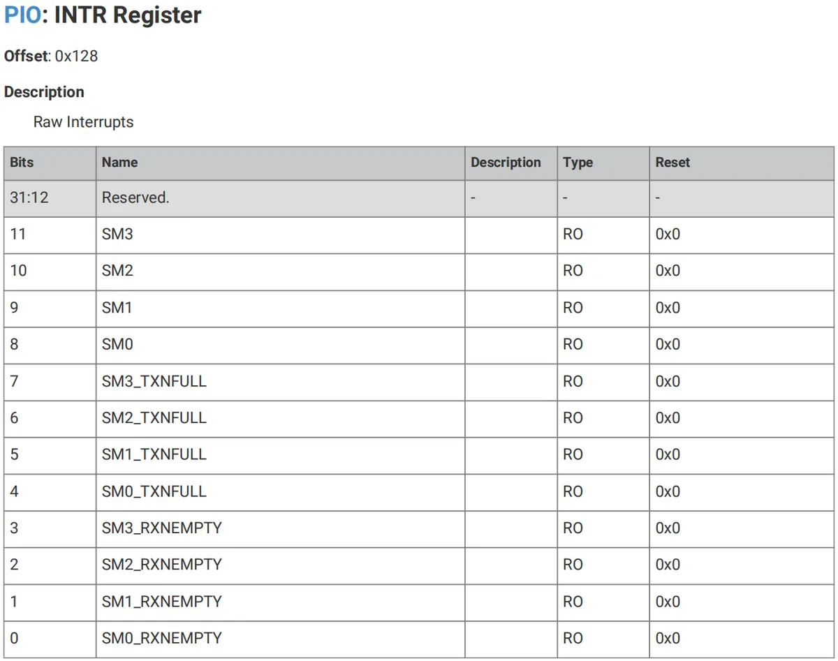
You can check the masked interrupt output status via the INTS register:
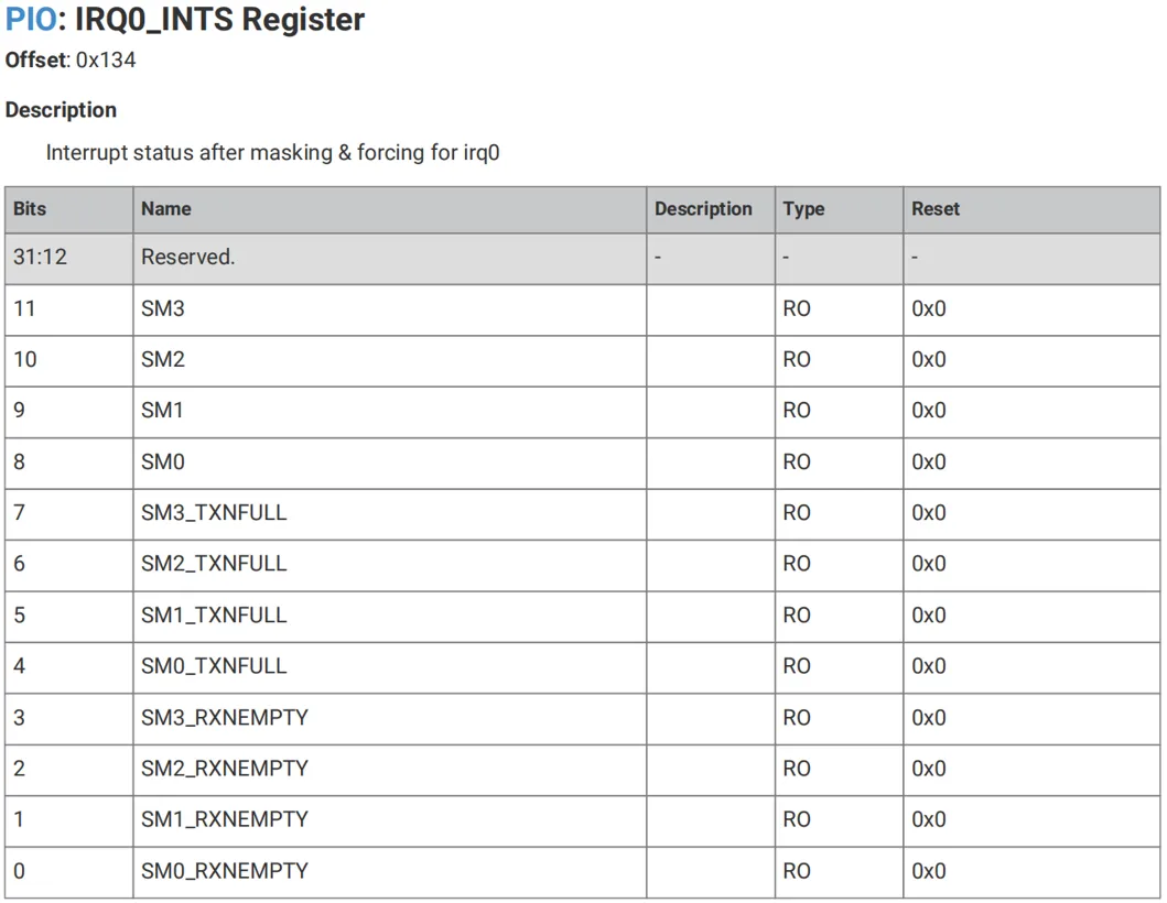
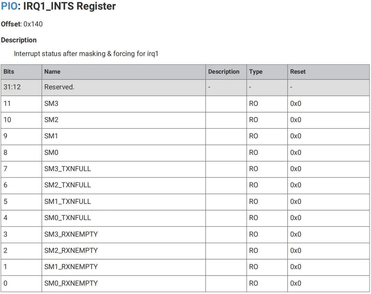
1.4.9 SET Instruction for Mapping GPIO Configuration
The SET mapping GPIO instruction is used to write data to GPIO pins (i. e., control high and low levels), and can also write data to X\Y registers.

Write the immediate value Data to Destination.
The parameters are defined as follows:
- Destination:
Destinationis a 3-bit configuration bit that specifies the write target of the 5-bit immediate operand; - Data:
Dataconsists of 5 configuration bits, which are fixed values written directly to the target, with a value range of 0 to 31 (the maximum value of 5-bit binary):- If the target is
PINS/PINDIRS: each bit of Data corresponds to one GPIO in the SET pin mapping, and a bit value of 1/0 corresponds to the high/low level (for PINS) or output/input direction (for PINDIRS) of the GPIO; - If the target is
X/Y: Data is directly used as the lower 5 bits of the register, and the upper 27 bits are cleared to 0. Therefore, the maximum value that can be initialized for X/Y via SET is 31 (suitable for short-period loop counting).
- If the target is
This instruction is used to set control signals, such as clock or chip select, or to initialize a loop counter. Since Data has only 5 data bits, the value that the erasable register can be SET to ranges from 0 to 31, allowing a maximum of 32 loops.
The pin mappings of SET and OUT are configured independently. They can be mapped to different positions — for example, one pin for clock signals and the other for data — and their pin ranges can also overlap: a UART transmission routine can use SET to set the start and stop bits, and use the OUT instruction to shift out FIFO data on the same pin.
The assembly syntax is as follows: set <destination>, <value>
Wherein:
<destination>is the destination for the aforementioned data operation;<value>is the value to be set, and its valid range is 0 to 31.
1.5 Detailed Explanation of PIO Functions and Features
1.5.1 Side-set Characteristics
The side-set feature is designed to simultaneously modify the level (by default) or direction of a specified GPIO while the main instruction is being executed, thus enabling parallel implementation of the main operation and GPIO control — for example, synchronizing "data output" with "clock toggling" in SPI, and "data transmission" with "SCL clock" in I2C.
| Advantage | Description | Typical scenario |
| Timing accuracy | The main instruction and GPIO control complete in the same clock cycle with no instruction delay, avoiding the timing skew caused by a separate SET instruction | Clock and data synchronization for SPI/I2C, timing control of high-speed serial communication |
| Compact code | No extra SET/OUT instructions are needed to control GPIO, which reduces the program instruction count and the state machine program memory used | High-frequency data transfer scenarios (such as SPI_TX_FAST) |
| Higher frequency | Fewer instruction execution cycles raise the maximum operating frequency the peripheral supports (for example, SPI can reach a higher clock frequency) | High-speed data transfer (such as SPI high-speed mode) |
| Mapping flexibility | The Side-set GPIO mapping is independent of the SET and OUT mappings and can overlap or be separate, supporting complex peripheral control logic | Independent control of I2C SDA/SCL, parallel output of multiple signals |
The behavior of Side-set is determined by the underlying hardware mechanism, which is the core difference between it and the SET/OUT instructions, as detailed below:
- Encoding location: the Delay/side-set
- Each instruction of PIO contains a 16-bit encoding, in which bits 12 to 8 (5 bits) serve as the
Delay/side-setmultiplexing field: - If configured as Delay: this field indicates the number of delay cycles (0~31) after the instruction is executed;
- If configured as Side-set: this field indicates the side-set data to be written to the GPIO (0~31, corresponding to up to 5 GPIOs);
- Field allocation is controlled by
PINCTRL_SIDESET_COUNT: if set to 1, it occupies 1 bit, leaving 4 bits available for delay; if set to 5, all 5 bits are used for sideset and delay is unavailable.
- Each instruction of PIO contains a 16-bit encoding, in which bits 12 to 8 (5 bits) serve as the
- Pin Mapping: Independent of SET/OUT, supports overlapping
- Side-set has a dedicated GPIO mapping configuration (
PINCTRL_SIDESET_BASE), which specifies the starting GPIO number for sideset control and is independent ofPINCTRL_SET_BASEfor SET andPINCTRL_OUT_BASEfor OUT; - The side-set GPIO mapping can overlap with the SET/OUT mapping (e. g., the same GPIO is used by OUT for data output and by side-set for clock control). In such cases, side-set takes priority over SET/OUT (if written simultaneously, the data from side-set shall prevail).
- Side-set has a dedicated GPIO mapping configuration (
- Effective Timing: Takes effect immediately, independent of the instruction pending status
- Regardless of whether the main instruction enters a waiting state (e. g., a PULL instruction waiting for data in the TX FIFO, or a PUSH instruction waiting for an empty space in the RX FIFO), the side-set data takes effect immediately in the first clock cycle of instruction execution;
- This ensures that the timing of GPIO control will not be delayed by the waiting of main instructions, which is the key to timing stability in high-speed communication.
- Compatibility: Supports all PIO instructions; any PIO instruction (OUT, IN, JMP, MOV, SET, PULL, PUSH, etc.) can be used in combination with Side-set, and the side-set data is specified via the
side <value>identifier following the instruction.
To use Side-set, you need to set 4 key options via the PIO configuration register to determine the bit count, activation rule, GPIO mapping and control type of the side-set, details are as follows:
| Configuration item | Corresponding register field | Function definition | Value / Description |
| 1. Side-set bit count | PINCTRL_SIDESET_COUNT | Defines the number of bits in the Delay/side-set field used for side-set (the remaining bits are used for delay) | 0~5: - 0: Side-set disabled; - 1~5: Number of bits used by side-set (e.g., 1 means 1-bit side-set, controlling at most 1 GPIO; 5 means 5-bit side-set, leaving no bits for delay) |
| 2. Enable bit | EXECCTRL_SIDE_EN | Determines whether Side-set requires the enable bit to take effect | - False (default): As long as SIDESET_COUNT>0, Side-set takes effect for all instructions; - True: Side-set takes effect only when the instruction sets the enable bit (used to enable side-set selectively) |
| 3. Starting GPIO number | PINCTRL_SIDESET_BASE | Defines the lowest GPIO number controlled by Side-set (bit 0 of side-set corresponds to this GPIO, bit n corresponds to SIDESET_BASE+n) | 0 to the maximum GPIO number (e.g., if set to 6, side-set bit 0 controls GPIO6 and bit 1 controls GPIO7) |
| 4. Control type (level / direction) | EXECCTRL_SIDE_PINDIR | Determines whether Side-set changes the GPIO level or the GPIO direction (input / output) |
The following is a line-by-line analysis of the spi_tx_fast program, combined with the configuration instructions for the practical use of Side-set:
.program spi_tx_fast ; defines a program named spi_tx_fast
.side_set 1 ; set the side-set data width to 1 bit

loop:
    out pins, 1 side 0 ; transfer 1 data bit to GPIO pin 1, and at the same time use the side-set operation to set it low
    jmp loop side 1 ; this instruction jumps back to the loop label, and at the same time the side-set operation sets it high
Combined with the program's. side_set 1, the 4 configuration items of this example are set as follows:
| Configuration item | Set value | Reason / Function |
| PINCTRL_SIDESET_COUNT | 1 | The program specifies a side-set width of 1 bit, controlling 1 GPIO (the SPI clock, CLK) |
| EXECCTRL_SIDE_EN | False | All instructions execute Side-set; no enable-bit filtering is needed |
| PINCTRL_SIDESET_BASE | Clock GPIO number (e.g., 6) | The GPIO controlled by side-set is the SPI CLK pin (GPIO6) |
| EXECCTRL_SIDE_PINDIR | False | It controls the level of the CLK pin (high / low), not the direction |
spi_tx_fast Example:
- Execution Timing: Each instruction occupies 1 system clock cycle.
out pins, 1 side 0During execution, data output is completed synchronously with the CLK going low.jmp loop side 1During execution, the jump is completed synchronously with the CLK going high. The entire loop takes only 2 clock cycles to output 1 bit of SPI data, enabling high-frequency data transmission. - Advantages: No additional SET instructions are required to control the CLK pin, leading to streamlined code; data and clock operate synchronously with zero timing deviation, and the maximum SPI frequency is significantly increased.
spi_tx_fast This example demonstrates two advantages of side-set: more precise alignment between data and clock, and faster overall program execution — in this case, one data bit can be output every two system clock cycles, while the program itself also takes up less space.
In I2C communication, the GPIO mapping and division of labor for Side-set, OUT, and SET are as follows, which reflects the flexibility of side-set:
- Side-set: SCL clock pin of I2C (responsible for clock flipping and synchronous data transmission);
- OUT: SDA data pin of I2C (responsible for shifting out data bits);
- SET: I2C's SDA data pin (responsible for generating pulses of special sequences such as Start/Stop); through this mapping division of labor, the finite-state machine can flexibly control the data output or special pulses of SDA while SCL provides the clock, and SDA/SCL can be mapped to any GPIO without being restricted by hardware pins.
Please note the following when using it:
- Resource contention between Delay and Side-set:
The Delay/side-setfields are multiplexed: the more bits occupied by the side-set, the fewer bits available for delay (e. g., if the side-set occupies 5 bits, delay cannot be used at all; if it occupies 1 bit, the maximum delay is 15 (4 bits)). - Priority Rule: If Side-set and SET/OUT write to the same GPIO at the same time, the data of Side-set will overwrite the data of SET/OUT. Therefore, the GPIO mapping needs to be reasonably planned according to the business scenario.
- Usage scenario of valid bits:
When EXECCTRL_SIDE_ENis set to true, only the Side-set of some instructions takes effect, which is applicable to scenarios requiring selective GPIO control (e. g., toggle the clock only during data transmission and perform no operation when idle). - Use of Direction Control:
When EXECCTRL_SIDE_PINDIRis set to true, Side-set modifies the GPIO direction, which is suitable for scenarios requiring dynamic switching of GPIO input/output (such as bidirectional communication on the SDA pin of I2C).
1.5.2 Program Wrap
Program Wrap is a hardware-level looping mechanism of the PIO finite-state machine, which essentially works by configuring dedicated registers (EXECCTRL_WRAP_BOTTOM and EXECCTRL_WRAP_TOP) to make the program counter (PC) automatically jump to the preset start address (WRAP_BOTTOM) instead of executing a software-level JMP jump instruction when it reaches the specified address (WRAP_TOP).This feature specifically addresses the instruction memory occupancy and execution cycle overhead caused by traditional JMP loops, and serves as a core hardware optimization method to improve the execution efficiency of PIO programs and save instruction memory.
If a PIO program uses the JMP instruction to implement outer loops (such as the repetitive steps for square wave generation or data transmission), it will have the following two notable drawbacks, which are also the core pain points that the program's loop-back feature is designed to address:
| Problem | Description | Impact |
| Wasted instruction memory | The JMP instruction occupies 1 separate instruction memory slot that could otherwise be used for other program logic | Reduces utilization of the limited PIO instruction memory (at most 32 instructions) |
| Execution cycle overhead | The JMP instruction itself consumes 1 clock cycle and breaks the continuity of instruction execution | Reduces the maximum execution speed of the program (e.g., the square-wave frequency is halved due to the cycle overhead of JMP) |
Taking the output of a square wave signal as an example, the code is as follows:
.program squarewave
    set pindirs, 1 ; step 1: set the pin to output mode (1 cycle)
again:
    set pins, 1 [1] ; step 2: set the pin high, delay 1 cycle (2 cycles in total: 1 for the instruction + 1 for the delay)
    set pins, 0 ; step 3: set the pin low (1 cycle)
    jmp again ; step 4: jump back to again (1 cycle)
This code implements a simple square wave signal generator. It generates a square wave by switching between high and low logic levels with an added delay. jmp jump instruction itself takes one clock cycle, and each set instruction also takes one cycle, so to ensure that the high and low level signals are held for the same duration, the set pins, 1 instruction adds a one-cycle delay, making the finite-state machine wait for one cycle before executing the set pins, 0 instruction. Each loop takes a total of 4 clock cycles.
Here, there are two issues:
JMPoccupies instruction memory that could otherwise be used by other programs- The additional cycles required to execute
JMPreduce the maximum output speed by half.
Since the program counter (PC) automatically wraps around to 0 when it exceeds 31, filling the entire instruction memory with set pins, 1 and set pins, 0 will solve the second problem, but this approach wastes a significant amount of memory.
The PIO assembler (pioasm) provides two dedicated assembler directives to mark the start and end positions of a loopback, which will eventually be mapped to the hardware registers (EXECCTRL control register), thus solving both of these problems:
| Assembler directive | Corresponding hardware register | Function definition |
| .wrap_target | EXECCTRL_WRAP_BOTTOM | Marks the start address of the program wrap (the PC jump target) |
| .wrap | EXECCTRL_WRAP_TOP | Marks the end address of the program wrap (the location where the PC triggers the wrap) |
Here is the upgraded version:
.program squarewave_wrap ; square wave program with wrap
    set pindirs, 1 ; initialization: set the pin to output mode (1 cycle)
.wrap_target ; marks the wrap start address (WRAP_BOTTOM = 1)
    set pins, 1 [1] ; Set pin high, delay 1 cycle (2 cycles total)
    set pins, 0 [1] ; set the pin low, delay 1 cycle (2 cycles in total)
.wrap ; marks the wrap end address (WRAP_TOP = 2)
The above code can remove the delay cycle, so that the output speed will be twice as fast as before, while maintaining equal durations for the high level and the low level:
- Execute
set pins, 1 [1](PC= 1). Upon completion, PC increments by 1 (PC= 2); - Execute
set pins, 0 [1](PC= 2). Upon completion, PC equalsWRAP_TOP(2), and the program automatically jumps toWRAP_BOTTOM(1) instead of incrementing PC by 1;
After executing an instruction in the program memory, the state machine updates the program counter using the following logic PC:
- If the current instruction is
JMPandConditionis true, setPCtoTarget - Otherwise, if
PCis equal toEXECCTRL_WRAP_TOP, setPCtoEXECCTRL_WRAP_BOTTOM - Otherwise,
PCis incremented by 1; however, if the current value is 31, it is set to 0
The . wrap_target and . wrap assembler directives in pioasm are effectively labels. They export constants to be written to WRAP_BOTTOM and WRAP_TOP respectively.
The sample code above, after being processed by the PIO assembler pioasm compile, will generate the following files:
// -------------------------------------------------- //
// This file is autogenerated by pioasm; do not edit! //
// -------------------------------------------------- //

#pragma once

# If PICO_NO_HARDWARE is not defined, the hardware/pio.h header file is included, which defines the PIO-related data structures and functions
#if !PICO_NO_HARDWARE
#include "hardware/pio.h"
#endif

// --------------- //
// squarewave_wrap //
// --------------- //

# The two macros define the positions of the .wrap_target and .wrap instructions in the program
#define squarewave_wrap_wrap_target 1
#define squarewave_wrap_wrap 2

# The array contains the instruction sequence of the squarewave_wrap program
static const uint16_t squarewave_wrap_program_instructions[] = {
    0xe081, // 0: set pindirs, 1
    // .wrap_target
    0xe101, // 1: set pins, 1 [1]
    0xe100, // 2: set pins, 0 [1]
    // .wrap
 };

# If PICO_NO_HARDWARE is not defined
#if !PICO_NO_HARDWARE
# Define a squarewave_wrap_program structure, which contains the program's instruction sequence, length, and other information
static const struct pio_program squarewave_wrap_program = {
    .instructions = squarewave_wrap_program_instructions,
    .length = 3,
    .origin = -1,
};

# Return a default state machine configuration, in which the positions of .wrap_target and .wrap are set
static inline pio_sm_config squarewave_wrap_program_get_default_config(uint offset) {
    pio_sm_config c = pio_get_default_sm_config();
    sm_config_set_wrap(&c, offset + squarewave_wrap_wrap_target, offset +
    squarewave_wrap_wrap);
    return c;
 }
#endif
We can see that the PIO assembler (pioasm) will convert. wrap_target and. wrap into constants and generate corresponding configuration functions, specifically including:
- Define
xxx_wrap_targetandxxx_wrapmacros to store the relative return address; - Generate
the pio_programstructure, which contains information such as the instruction sequence and its length; - Generate
xxx_program_get_default_configfunction, which automatically writes the return address topio_sm_config(by calling thesm_config_set_wrapfunction).
When using the program loopback feature, please note the following:
- Address Absoluteness:
WRAP_BOTTOMandWRAP_TOPare absolute addresses of the PIO instruction memory, not relative addresses; - Offset Adjustment: If the program is loaded to a non-zero offset position in the instruction memory (e. g., offset= 5), the relative address of the return branch shall be added with the offset to obtain the absolute address before being written into the register;
- Direct register configuration: If the default configuration function is not used, you can directly use the
pio_sm_set_wrapfunction or modify theEXECCTRLregister'sWRAP_BOTTOM/WRAP_TOPfields to configure the wrap address.
It is also necessary to note that:
- Range restriction for wrap-around addresses:
WRAP_BOTTOMmust be less than or equal toWRAP_TOP, and neither of them may exceed the maximum address (31) of the PIO instruction memory; otherwise, the wrap-around logic will fail. - Compatibility with JMP Instructions: The program loopback mechanism does not affect the execution of JMP instructions (as JMP has a higher priority), so JMP can be used inside a loopback loop to implement conditional branching, balancing loop efficiency and logical flexibility.
- Priority of natural wrap-around: If program wrap-around is not configured (
WRAP_BOTTOM= 0 andWRAP_TOP= 31), the PC will automatically reset to 0 when it reaches 31. This is the natural wrap-around feature of the PIO instruction memory, which can be regarded as the default case of program wrap-around. - Compatibility of Delay and Side Sets: The loopback logic only affects the update of the PC, and does not affect the instruction delay (
[n]) or side set (side n) features; both the delay and side set will still take effect normally.
1.5.3 FIFO Merge
The default FIFO of each PIO finite-state machine is "bidirectional double buffer":
| FIFO type | Data direction | Depth | State machine instruction |
| TX FIFO | System → state machine | 4 words | PULL (read) |
| RX FIFO | State machine → system | 4 words | PUSH (write) |
| This structure suits bidirectional data transfer, but if a program only needs one-way transfer (e.g., send-only UART-TX or receive-only UART-RX), the other FIFO sits idle, wasting resources. |
However, many programs do not require bidirectional data transmission between the system and the finite-state machine, while a longer FIFO is very useful, especially in high-bandwidth interfaces such as DPI image transmission. In these cases, you can use the SHIFTCTRL_FJOIN option to combine two 4-word-long FIFOs into one 8-word-long FIFO.
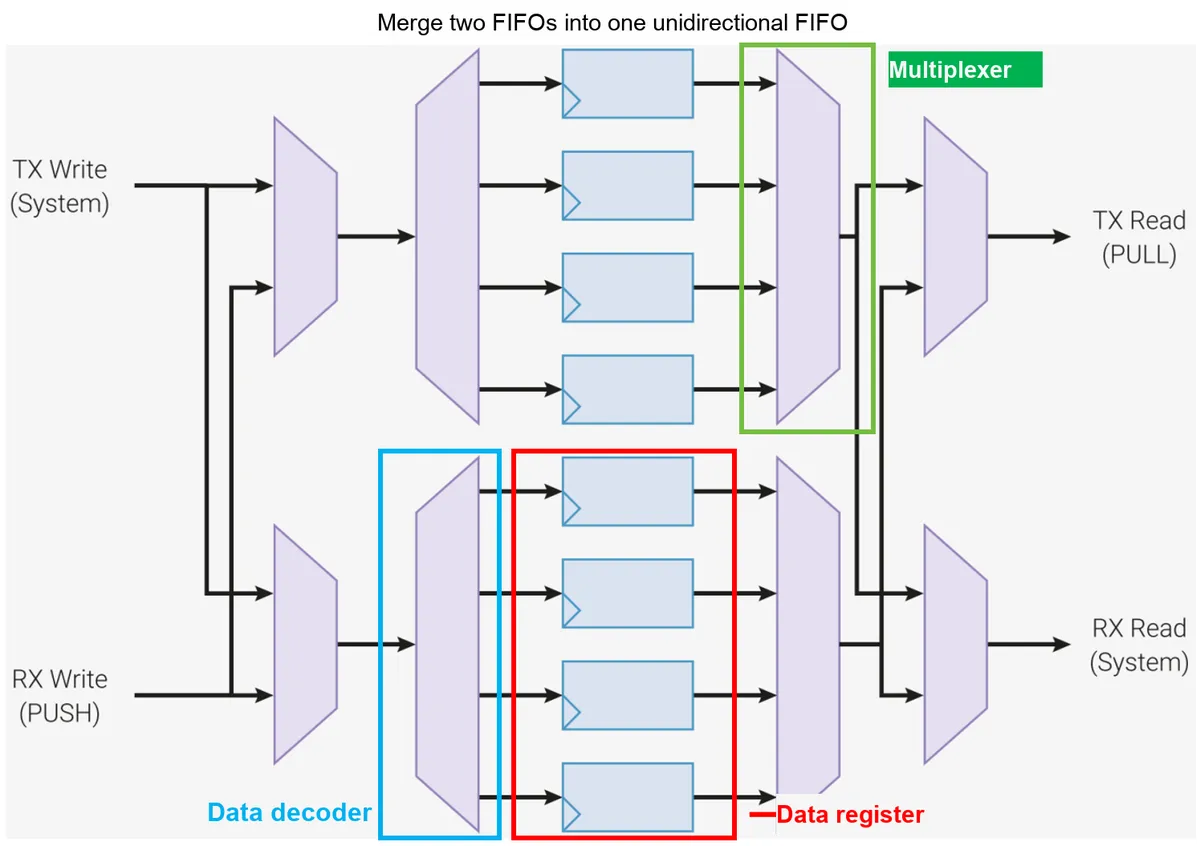
The essence of FIFO merging is to integrate two 4-word FIFO resources into one 8-word unidirectional FIFO, which has two core values:
- Increase FIFO depth: Increasing it from 4 words to 8 words allows more data to be buffered temporarily, reducing the frequency of system interrupts (for example, during UART reception, a deeper FIFO eliminates the need to frequently trigger interrupts to fetch data);
- Avoid resource waste: In unidirectional transmission scenarios, idle FIFO resources can be fully utilized (for example, when only the TX finite-state machine is used, the RX FIFO can also be converted to a TX FIFO).
The hardware structure of FIFO merging consists of a data decoder and a multiplexer (corresponding to the diagram you provided titled "Merge Two FIFOs into a Unidirectional FIFO"), and its working process is as follows:
- Data Writing: When the system writes data to the FIFO via "TX Write" or "RX Write", the data decoder will allocate the data to the corresponding original FIFO (the original TX or RX FIFO);
- Data Read: The merged FIFO passes through a multiplexer, which "merges" the data from the original TX FIFO and original RX FIFO into a single data stream for the finite-state machine to access via
PULLread operations (when merged as a TX FIFO), or for system read operations (when merged as an RX FIFO); - Unidirectional Multiplexing: After merging, only the "all-TX" or "all-RX" mode can be selected; in this case, the FIFO resources in the other direction will be multiplexed as the buffer for the current direction, ultimately forming an 8-word unidirectional FIFO.
The merged FIFO provides a 1:4 data decoder and a 4:1 multiplexer, enabling us to perform write and read operations between the TX and RX channels of the FIFO, so that all 32-bit × 8-word data can be accessed from both ports.
UART is a typical scenario of "unidirectional finite-state machine implementation"(the TX and RX channels use independent finite-state machines respectively):
- Default case: The TX finite-state machine uses its own 4-word TX FIFO, the RX finite-state machine uses its own 4-word RX FIFO, and the other FIFO of both sides is idle;
- After merging:
- The TX finite-state machine can combine its own TX+ RX FIFO into an 8-word TX FIFO, which can temporarily store more data to be transmitted and reduce the number of interrupts for the system to write to the FIFO;
- The RX finite-state machine can merge its own RX+ TX FIFO into an 8-word RX FIFO, which can temporarily store more received data and eliminates the need for the system to frequently interrupt to fetch data; ultimately, the UART with an 8-word FIFO handles interruptions at only half the frequency of that with a 4-word FIFO, improving system efficiency.
After merging the FIFOs, the FIFO of the finite-state machine will become a structure of "unidirectional 8 words + 0 words", and the corresponding states and instruction behaviors will change:
- FIFO Status: The FIFO status is indicated by the
FSTAT register(the second figure you provided). After merging, the "unused FIFO" will be in both the FULL and EMPTY states simultaneously:- If combined as TX FIFO (8 words):
- TX FIFO works properly,
FSTAT.TXEMPTY/TXFULLindicates the actual status; - RX FIFO is disabled,
FSTAT.RXEMPTYandRXFULLwill be set to 1 simultaneously (indicating that the RX FIFO is both full and empty and thus unavailable);
- TX FIFO works properly,
- If combined into RX FIFO (8 words):
- RX FIFO operates normally,
FSTAT.RXEMPTY/RXFULLindicates the actual status; - When TX FIFO is disabled,
FSTAT.TXEMPTYandTXFULLwill be set to 1 simultaneously.
- RX FIFO operates normally,
- If combined as TX FIFO (8 words):
- Impact of finite-state machine instructions: After merging, the instructions corresponding to the disabled FIFO will fall into a permanent waiting state:
- When merged into TX FIFO: the finite-state machine executes the
PUSHinstruction (writing data to the RX FIFO) and keeps waiting (since the depth of the RX FIFO is 0, writing is impossible); - When merged into the RX FIFO: the finite-state machine executes
the PULLinstruction (to read data from the TX FIFO) and keeps waiting (since the depth of the TX FIFO is 0, there is no data available to read).
- When merged into TX FIFO: the finite-state machine executes the
It should be noted that when merging FIFOs or splitting merged FIFOs, all data in the FIFO of the current finite-state machine will be discarded. If the data cannot be recovered, the FIFO queue must be emptied in advance.
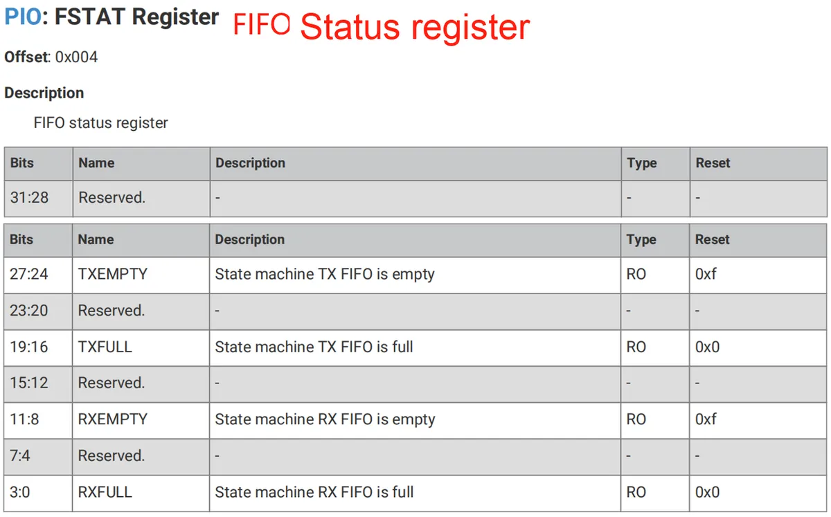
An 8-word deep FIFO is sufficient to work with the RP2040's DMA to achieve the high transfer rate of "1 byte per clock cycle"(as long as the DMA is not blocked by other tasks).
1.5.4 Automatic Ejection and Automatic Loading
First, let's review the "shift and data replenishment" logic of the two core registers:
- OSR (Output Shift Register): The finite-state machine shifts out data via the OUT instruction. After the data is shifted out, the OSR will become "empty" and needs to be replenished with new data from the TX FIFO (the buffer from the system to the finite-state machine) manually using the PULL instruction;
- ISR (Input Shift Register): The finite-state machine shifts data in via the IN instruction; after the shifting operation completes, the ISR becomes "full", and the data needs to be pushed to the RX FIFO (the buffer from the finite-state machine to the system) manually using the PUSH instruction.
The core of automatic push/load is to let the hardware automatically complete the operations of "supplementing OSR data" and "pushing ISR data" without manually writing PULL/PUSH instructions, which not only saves instruction memory but also improves data transmission efficiency.
First, let's look at a sample program for manually loading OSR data and analyze its drawbacks:
.program manual_pull
.side_set 1 opt ; set the Side-set width to 1 bit; opt makes specifying side <value> optional for instructions

.wrap_target ; marks the target position of the .wrap instruction
    set x, 2 ; initialize register x to 2; this register is used to control the number of loops
    pull side 1 [1] ; perform a manual pull; if there is no TX data, it waits here
bitloop: ; a label is defined here, used to loop over outputting data bits
    out pins, 1 side 0 [1] ; shift 1 data bit out to the GPIO pin, and at the same time set Side-set to 0, used to control the clock
    jmp x-- bitloop side 1 [1] ; decrement register x; if it is not 0, jump back to the bitloop label
    out pins, 1 side 0 ; output the last data bit, with Side-set set to 0
.wrap ; unconditionally jump back to the position marked by .wrap_target
This program shifts out 4 data bits from each FIFO word at a rate of 1 data bit per 4 clock cycles, while outputting a clock signal. When the TX FIFO is empty, the program pauses at the high level of the clock (note that the side-set remains active during the cycle in which the instruction is paused).
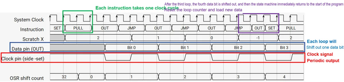
This program has a number of limitations:
- High instruction slot occupancy: only 2 out of 5 instruction slots are used for actual data output, while the rest are reserved for counter initialization, manual PULL operations and jumps;
- Low throughput: only 1 bit of data can be shifted out every 4 system clock cycles, and the speed is limited by the cycle overhead of manual instructions;
- Poor flexibility: The number of bits to be shifted out is fixed (depending on the X counter), so it cannot be dynamically adapted to different data lengths.
At this point, we can enable the autopush data auto-push and autopull data auto-load functions:
- The core of automatic loading is: the hardware tracks the "shift counter" of the OSR. When the number of shifted-out bits reaches the configured threshold, data is automatically loaded from the TX FIFO to the OSR without manual
PULL; - The logic of automatic push is symmetrical to that of automatic loading: the hardware tracks the "shift counter" of the ISR, and when the number of shifted-in bits reaches the configured threshold, it automatically pushes the ISR data to the RX FIFO without manual
PUSH.
Enable autopush data auto-push: when the count threshold of the set shift counter is reached, the finite-state machine will automatically execute the IN instruction to load data from the ISR register and push it to the RX FIFO, and meanwhile clear the corresponding data in the ISR register:
- The finite-state machine executes
OUTinstruction, and the OSR shift counter accumulates the number of bits shifted out; - When the counter reaches
SHIFTCTRL_PULL_THRESH(the configured threshold), the hardware automatically triggersPULL; - Read one 32-bit data from the TX FIFO (Transmit FIFO Memory) and load it into the OSR output shift register;
- The OSR shift counter is cleared and waits for the next round of shifting out.

After enabling automatic rollout, the code is as follows:
.program autopull
.side_set 1 ; side-set width is 1 bit

.wrap_target
    out pins, 1 side 0 [1] ; shift out 1 data bit, set side-set clock to 0
    nop side 1 [1] ; no operation, set side-set clock to 1 (replaces a manual jump)
.wrap
Advantages of this program:
- More streamlined instructions: only 2 instructions, with no counter or jump logic involved;
- 2x speedup: eliminates the periodic overhead caused by manual PULL operations and jumps; if latency is removed, the throughput can reach "1 bit shifted out per 2 system clock cycles";
- High flexibility: The number of shift bits is controlled by the hardware threshold (rather than code) and can be dynamically configured as 16/32 bits.
Enable autopull data auto-loading: when the count threshold of the set shift counter is reached, the finite-state machine will automatically execute the OUT instruction to load data from the FIFO. By enabling data auto-loading, compared with manually executing the OUT instruction, it can save the time for loading the OUT instruction and achieve higher data throughput at the same time:
- The finite-state machine executes
INinstructions, and the ISR shift counter accumulates the number of bits shifted in; - When the counter reaches
SHIFTCTRL_PUSH_THRESH(the configured threshold), the hardware automatically triggersPUSH; - The 32-bit data of the ISR input shift register is pushed into the RX FIFO (receive FIFO memory);
- The ISR shift counter is cleared and waits for the next round of shifting-in.
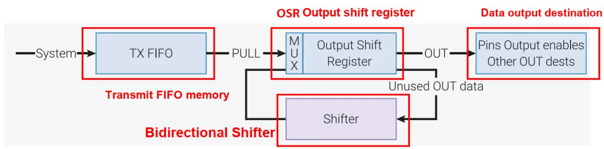
By using the autopull feature, manual_pull the example can be rewritten as follows:
.program autopull
.side_set 1

.wrap_target
    out pins, 1    side 0      [1]
    nop            side 1      [1]
.wrap
This program is shorter and simpler than the original version, and runs twice as fast when the delay is removed, because automatically loading the OSR via hardware does not consume clock cycles during instruction execution. Note that the program does not know how many data bits need to be shifted before the next load; the hardware will automatically load once the configured threshold (SHIFTCTRL_PULL_THRESH) is reached, so the example program can also shift out 16 data bits or 32 data bits from each FIFO word.
Finally, note that the above program is not completely identical to the original one: it will pause when the clock signal (note that this is not the system clock, but the communication clock) is low, rather than when it is high. This behavior is mainly caused by the design feature of the PIO finite-state machine, which executes instructions based on clock pulse edges. In the out pins, 1 side 0 [1]instruction, data output occurs on the falling edge of the clock signal, while the nop side 1 [1]instruction is executed on the rising edge of the clock signal.Therefore, when the TX FIFO is empty, the finite-state machine pauses during the low level phase of the clock signal, and resumes execution only after new data enters the TX FIFO.
We can adjust the pause position via the PULL IFEMPTY instruction, which uses the same configurable threshold as autopull; after using this instruction, it can simplify certain programs to control where the pause occurs, just like autopull does. When both the OSR and TX FIFO are empty, the finite-state machine will enter a paused state while executing OUT.
.program somewhat_manual_pull
.side_set 1

.wrap_target
    out pins, 1    side 0      [1]
    pull ifempty   side 1      [1]
.wrap
Below is a complete example, including a PIO program and a C program that loads and runs it, demonstrating how to enable both autopull and autopush simultaneously on the same finite-state machine. The function of finite-state machine 0 is to transfer data from the TX FIFO to the RX FIFO, with a throughput of one byte every two clock cycles.
The PIO program is as follows:
.program auto_push_pull ; defines a program named auto_push_pull

.wrap_target
    out x, 32 ; automatically push (auto-push) 32 bits of data from register x to the TX FIFO
    in x, 32 ; automatically pull (auto-pull) 32 bits of data from the RX FIFO into register x
.wrap
A C program for loading and running PIO programs
#include "tb.h" // TODO this is built against existing sw tree, so that we get printf etc

#include "platform.h"
#include "pio_regs.h"
#include "system.h"
#include "hardware.h"

#include "auto_push_pull.pio.h"

int main()
{
    // Used to initialize the test environment
    tb_init();

    // Load and configure PIO state machine 0 to run the auto_push_pull program
    // Load the instructions in the auto_push_pull_program array into PIO instruction memory
    for (int i = 0; i < count_of(auto_push_pull_program); ++i)
        mm_pio->instr_mem[i] = auto_push_pull_program[i];

    // Configure the SHIFTCTRL register of state machine 0
    // Enable auto-push and auto-pull, and set the push and pull thresholds to 32
    mm_pio->sm[0].shiftctrl =
            (1u << PIO_SM0_SHIFTCTRL_AUTOPUSH_LSB) |
            (1u << PIO_SM0_SHIFTCTRL_AUTOPULL_LSB) |
            (0u << PIO_SM0_SHIFTCTRL_PUSH_THRESH_LSB) |
            (0u << PIO_SM0_SHIFTCTRL_PULL_THRESH_LSB);

    // Configure the EXECCTRL register of state machine 0, and set the positions of the .wrap_target and .wrap instructions
    mm_pio->sm[0].execctrl =
            (auto_push_pull_wrap_target << PIO_SM0_EXECCTRL_WRAP_BOTTOM_LSB) |
            (auto_push_pull_wrap << PIO_SM0_EXECCTRL_WRAP_TOP_LSB);

    // Start state machine 0
    hw_set_bits(&mm_pio->ctrl, 1u << (PIO_CTRL_SM_ENABLE_LSB + 0));

    // Write 5 data items to the TX FIFO, and read and print 5 data items from the RX FIFO
    for (int i = 0; i < 5; ++i)
        mm_pio->txf[0] = i;
    for (int i = 0; i < 5; ++i)
        printf("%d\n", mm_pio->rxf[0]);

    return 0;
}
The following figure shows the entire execution process of the finite-state machine:
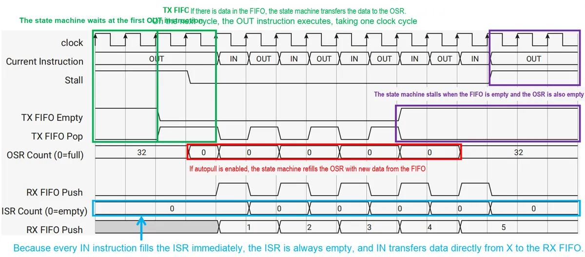
To trigger auto-expansion or auto-load at the correct time, the finite-state machine uses a pair of 6-bit shift counters to track the total number of shifts for ISR and OSR:
- After a reset, or when
CTRL_SM_RESTARTis triggered, the ISR shift counter is set to 0 (no data has been shifted in yet), and the OSR shift counter is set to 32 (no data is pending to be shifted out); OUTinstruction increments the OSR shift counter byBit count;INinstruction increments the shift counter of the ISR byBit count;PULLinstruction or automatic loading will clear the OSR counter to 0;The PUSHinstruction or an automatic pop operation will clear the ISR counter to 0;MOV OSR, xorMOV ISR, xwill clear the OSR or ISR shift counter to 0;OUT ISR, ninstruction sets the ISR shift counter ton.
When executing any OUT or IN instruction, the finite-state machine compares the shift counter with SHIFTCTRL_PULL_THRESH and SHIFTCTRL_PUSH_THRESH to determine whether to take action. Auto-pull and auto-push are enabled by the SHIFTCTRL_AUTOPULL and SHIFTCTRL_AUTOPUSH fields respectively.
1.5.4.1 Detailed Explanation of Auto Push (autopush)
Below is the pseudocode for the IN instruction with autopush enabled:
// Read the data and shift it into the isr shift register using the in instruction
isr = shift_in(isr, input())
// Update the value of the isr shift counter; it increases by one for each data item read
// When isr count is greater than 32, it is set to 0
isr count = saturate(isr count + in count)

// Check whether the received bit count rx count has reached the preset threshold
if rx count >= threshold:
    // If the RX FIFO is full, stall program execution (stall)
    if rx fifo is full:
        stall
    // If the RX FIFO is not full
    else:
        // Push the data in isr out to the RX FIFO
        push(isr)
        // Reset isr and isr count to 0, ready to receive the next data packet
        isr = 0
        isr count = 0
Note that the hardware platform only requires one machine clock cycle to execute the above steps (unless the finite-state machine pauses).
1.5.4.2 Detailed Explanation of Auto-loading: autopull
During cycles in which no OUT instruction is executed, the hardware executes the following pseudocode:
// If a MOV or PULL instruction was executed
if MOV or PULL:
    // Reset the bit count osr count of the output shift register (OSR) to 0
    osr count = 0

// Check whether the OSR bit count osr count has reached the preset threshold
if osr count >= threshold:
    // If the TX FIFO is not empty
    if tx fifo not empty:
        // Pull (PULL) data from the TX FIFO into the OSR
        osr = pull()
        // Reset osr count to 0, ready for the next transmission
        osr count = 0
Therefore, auto-loading can occur at any point between two OUT instructions, depending on when the data arrives at the FIFO.
During the cycle of executing the OUT instruction, the steps are slightly different:
// Check whether the bit count osr count of the output shift register (OSR) has reached the preset threshold
if osr count >= threshold:
    // If the TX FIFO is not empty
    if tx fifo not empty:
        // Pull (PULL) data from the TX FIFO into the OSR
        osr = pull()
        // Reset osr count to 0, ready for the next transmission
        osr count = 0
    // Whether or not the TX FIFO is empty, stall program execution once the preset threshold is reached
    stall
// If osr count has not reached the threshold
else:
    // Output the data in the OSR
    output(osr)
    // Shift the OSR left by out count bits, and fill the low bits with new data
    osr = shift(osr, out count)
    // Update osr count; when osr count is greater than 32, it is set to 0
    osr count = saturate(osr count + out count)

    // Check again whether osr count has reached the threshold
    if osr count >= threshold:
        // If the TX FIFO is not empty
        if tx fifo not empty:
            // Pull data from the TX FIFO into the OSR, and reset osr count to 0
            osr = pull()
            osr count = 0
Hardware can fill the OSR while shifting out all data, as these two operations can be executed in parallel. However, hardware cannot perform both OSR filling and 'OUT' of the same data in the same cycle, as this would result in an excessively long logic chain. It can be considered that for the program, the filling operation is asynchronous, but 'OUT' acts as a data barrier: the finite-state machine must never OUT data that has not yet been written to the FIFO.
Note that when auto-loading is enabled, the operation of copying data from the OSR 'MOV' is undefined; depending on the competition status with the system DMA, you may read residual data that has not yet been moved out, or new data from the FIFO. Similarly, the 'MOV' operation to the OSR may overwrite the data that has just been automatically loaded. However, the data 'MOV' into the OSR will never be overwritten, because 'MOV' updates the shift counter.
If you do need to read the content of the OSR, you should explicitly perform some kind of 'PULL'. The indeterminacy described above is the cost of automatic loading by hardware. Enabling automatic loading changes the behavior of 'PULL': if the OSR is full, a PULL is an invalid operation. This is done to avoid race conflicts with system DMA. It acts like a barrier: either the automatic loading has already started executing, in which case the 'PULL' operation is invalid; or the program will wait at the 'PULL' instruction until there is data in the FIFO.
1.5.5 PIO-specific clock divider
PIO operates based on the system clock, but for the vast majority of interfaces, the system clock runs too fast, and the number of insertable Delay cycles is limited. For devices such as UART that require precise control and adjustment of signal rates, it is ideal that multiple finite-state machines running the same program can also adjust their rates independently. Therefore, each finite-state machine is equipped with a clock divider.
The clock divider does not reduce the system clock rate; instead, it defines how many system clock cycles correspond to "one cycle" of executing a PIO program. It generates a clock enable signal that can pause or resume execution in each system clock cycle. The essence of the clock divider is to generate a "Clock Enable signal" to control the execution rhythm of the finite-state machine:
- When Clock Enable is high, the finite-state machine executes one instruction;
- When Clock Enable is low, the finite-state machine pauses execution (while the system can still access its FIFO and modify the configuration).
A clock divider can simplify the interface between the finite-state machine and the system, reduce latency, and occupy a very small chip area. When the clock enable signal is at a low level, the finite-state machine is completely in an idle state, but the system can still access the FIFO of the finite-state machine and change its configuration.
The clock divider supports division with 16 integer data bits and 8 fractional data bits, and the fractional divider adopts a first-order delta-sigma structure. The clock division ratio can be adjusted in increments of 1/256 within the range of 1 to 65536.
If the clock division ratio is set to 1, the finite-state machine will execute in every clock cycle, that is, run at full speed:

Typically, using only an integer frequency divider causes the finite-state machine to execute at a rate where n clock cycles equal 1 execution cycle, resulting in an effective clock rate of f (sys) / n.
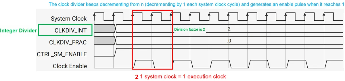
When a more precise rate (e. g., 2.5x frequency division) is required, integers alone are insufficient; in this case, fractional frequency division is adopted, which realizes the mapping of "a non-integer number of system clocks to one execution cycle" through the combination of "integer part + fractional part", and the value of the fractional frequency divider equals n + f / 256, where n and f are the integer and fractional parts of the CLKDIV register of this finite-state machine. It selectively extends a certain division period between n cycles and n+ 1 cycles.
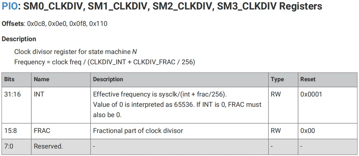
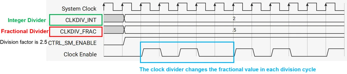
We can see that:
- The actual frequency division ratio of the frequency divider = integer part (
INT) + fractional part (FRAC/256)(FRACis 8-bit, ranging from 0 to 255, corresponding to a decimal between 0 and 1); - Adopt the "first-order integral-differential (delta-sigma)" algorithm: use n system clocks in most cycles and occasionally n+ 1 system clocks, so as to realize a fractional division ratio on average.
- In the figure:
- The integer part INT = 2, and the fractional part FRAC = 128 (since 0.5 = 128/256);
- The frequency divider generates enable pulses alternately using 2 and 3 system clocks, which averages out to 2.5 system clocks per execution cycle;
When the integer division value n is small, the jitter caused by the fractional division ratio may be unacceptable. However, when the integer division value n is very large, the jitter is almost negligible.
It should be noted that for high-speed asynchronous serial ports, it is recommended to use an even frequency division ratio or an integer multiple of 1 Mbaud rate instead of the traditional multiple of 300 to avoid unnecessary jitter.
1.5.6 GPIO Mapping
GPIO mapping refers to the hardware connection rules between PIO finite-state machines and external GPIO pins, which are categorized into two types: "output mapping (finite-state machine → GPIO)" and "input mapping (GPIO → finite-state machine)". It determines the specific GPIO pins controlled or read by finite-state machine instructions (OUT/SET/side-set/IN), and serves as a core flexible feature for PIO to adapt to the pin layouts of different peripherals.
Internally, the PIO has a 32-bit register that represents the output level of each GPIO pin it can drive, and another register that indicates the enable state (high or low impedance) for each output;During each system clock cycle, each finite-state machine can write to some or all of the GPIOs in these registers.
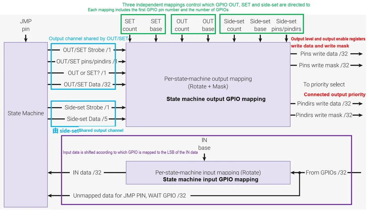
The write data and write mask of the output level and output enable register come from the following sources:
- An
OUTinstruction can write up to 32 data bits. Depending on theDestinationfield of the instruction, the instruction can be applied to the pin or pin direction. The lowest bit of theOUTdata maps to thePINCTRL_OUT_BASE, sequentially mapsPINCTRL_OUT_COUNTdata bits backward, and returns after reaching GPIO31. - A single
SETinstruction can hold a maximum of 5 data bits. Depending on theDestinationfield, this instruction can be applied to either the pin state or the pin direction.The least significant bit of theSETdata is mapped toPINCTRL_SET_BASE, with the subsequent bits mapped sequentially for a total ofPINCTRL_SET_COUNT bits, wrapping around after reaching GPIO31. - A single
side-setoperation can write a maximum of 5 data bits. Depending on the value of theEXECCTRL_SIDE_PINDIRregister field, this operation can be applied to either pin values or pin directions. The least significant bit of the side-set data maps toPINCTRL_SIDESET_BASE, with subsequent bits mapping backward in sequence for a total ofPINCTRL_SIDESET_COUNTdata bits, wrapping around after reaching GPIO31.
Each OUT / SET /side-set operation writes to a consecutive pin range, but each range has its own independent size and location within the 32-data-bit GPIO space. This is already sufficiently flexible for most applications. For example, if one finite-state machine implements an interface such as SPI on one set of pins, another finite-state machine can run the same program, mapped to a different set of pins, to provide a second SPI interface.
During any clock cycle, a finite-state machine can execute one OUT or SET, and can simultaneously execute one side-set. The pin mapping logic generates a write mask of 32 data bits, and writes the output level and output enable registers to the data bus according to the request content and pin mapping configuration.
If the side-set operation of the same finite-state machine within the same clock cycle overlaps with the OUT / SET operation, side-set takes precedence in the overlapping region.
1.5.6.1 Output Priority
Output Mapping Control OUT / SET / side-set instructions correspond to the GPIO pins, and the core rules are as follows:
- Independent mapping interval configuration:
OUT/SET/side-seteach configure their mapping ranges via dedicated registers:OUT: Determined byPINCTRL_OUT_BASE(starting GPIO number) andPINCTRL_OUT_COUNT(number of pins). The least significant bit of the data corresponds toOUT_BASE, and subsequent GPIOs are mapped in sequence (wrapping around after GPIO31);SET: determined byPINCTRL_SET_BASEandPINCTRL_SET_COUNT, following the same rule as OUT;side-set: determined byPINCTRL_SIDESET_BASEandPINCTRL_SIDESET_COUNT, following the same rules as OUT;
- Operation priority in the same cycle: If a finite-state machine executes
side-setandOUT/SETwithin the same clock cycle, and the GPIO pins mapped by the two overlap, the side-set operation takes effect first (overwriting the corresponding pin values of OUT/SET); - Write Data and Mask: Each output operation generates 32-bit "write data" and "write mask"; only the GPIOs covered by the mask will be modified, while the GPIOs not covered will retain their original state.
1.5.6.2 Output Priority
Each finite-state machine selects the priority via a write mask for each GPIO. For each GPIO, the write levels and directions from the four finite-state machines are considered, and then the values from the finite-state machine with the highest number are applied.
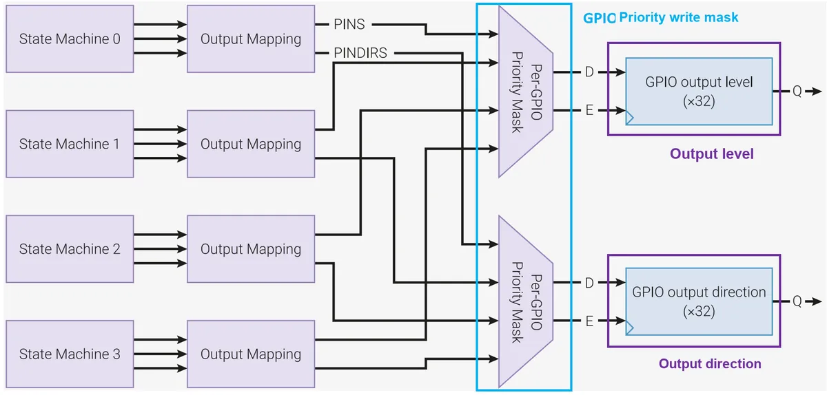
Each finite-state machine executes once per cycle via its pin mapping hardware OUT / SET and side-set. In this way, each finite-state machine generates 32 data bits of write data and a write mask for the GPIO output level and output enable registers.
For each GPIO, the PIO accounts for write operations from all four finite-state machines, then applies the write operation from the finite-state machine with the highest number. This step is performed separately for the output level and output value, so it is possible for a single finite-state machine to change both the level and direction of the same pin within the same cycle (for example via simultaneously issued SET and side-set), or for one finite-state machine to change the GPIO direction while another finite-state machine changes the level of the same GPIO. If no finite-state machine writes to the level or direction of a GPIO, the value remains unchanged.
1.5.6.3 Input Mapping
IN The way the instruction receives data is that the LSB is mapped to the GPIO set by PINCTRL_IN_BASE, subsequent higher bits come from GPIOs with sequentially higher numbers, and the sequence wraps around when reaching bit 31.
In other words, the IN bus is the result of right-shifting the GPIO input values by the value specified in PINCTRL_IN_BASE. If there are fewer than 32 GPIOs, the PIO input will be padded with 0s at the corresponding positions to make up the full 32 data bits.
Instructions such as like WAIT GPIO use the absolute GPIO numbering instead of the index in the IN data bus, and no right shift is performed in this case.
1.5.6.4 Input Synchronizer
To ensure the stability of PIO, each GPIO input is equipped with two standard 2-flip-flop synchronizers, which results in a two-cycle delay in input sampling; however, the advantage is that the finite-state machine can execute IN PINS at any time, and only sees clean high and low levels without intermediate values that may interfere with the finite-state machine circuit. This is particularly critical for asynchronous interfaces such as UART RX.
Sometimes, certain GPIOs may need to bypass the synchronizer. This reduces latency, but the user must ensure on their own that the finite-state machine does not sample at the wrong time. Typically, only synchronous interfaces such as SPI can achieve this. Set the INPUT_SYNC_BYPASS corresponding data bit to bypass the synchronizer.
Note that sampling unstable inputs will lead to unpredictable finite-state machine behavior, and this situation should be avoided.
We can configure or read the synchronizer by reading from and writing to the INPUT_SYNC_BYPASS register:
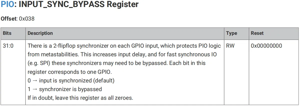
1.5.7 Instruction Execution
In addition to the instruction memory, the finite-state machine can also execute instructions from three other sources:
MOV EXECcan execute instructions from a register specified bySource:MOV EXEC, <source>takesthe 16-bit data from source(e. g., X/Y/ISR/OSR) and executes it as an instruction;- The MOV instruction consumes 1 cycle, and the instruction in the register is executed in the next cycle.
OUT EXECcan execute the data migrated by OSR:OUT EXEC, <bit_count>Executes the 16-bit data shifted out from the OSR as an instruction;- The OUT instruction consumes 1 cycle, and this instruction will be executed in the next cycle.
- Execute instructions from the
SMx_INSTRcontrol register; the system can directly write instructions to this register for immediate execution:- Fetch: Obtain the instruction pointed to by the current program counter (PC);
- Write: Write a 16-bit instruction to the register, and the finite-state machine will execute the instruction immediately.
In the following example program, we load 32 data bits from the TX FIFO in a loop, then execute the lower 16 data bits as an instruction (since a 32-bit instruction will be written to the INSTR register, and only the lower 16 bits of the INSTR register are accessible).
The PIO program is as follows:
.program exec_example

hang:
    jmp hang ; defines a label hang, and forms an infinite loop jump here
execute:
    out exec, 32
    jmp execute ; defines another label execute, where the 32-bit data in the register is output and executed in an infinite loop

.program instructions_to_push

    out x, 32 ; output 32 bits of data from register x
    in x, 32 ; load 32 bits of data from the input port into register x
    push ; push the data in register x to the TX FIFO
The C language program for calling the PIO program is as follows, and this program will output "12345678" when running:
#include "tb.h" // TODO this is built against existing sw tree, so that we get printf etc

#include "platform.h"
#include "pio_regs.h"
#include "system.h"
#include "hardware.h"

#include "exec_example.pio.h"

int main()
{
    tb_init();

    // Load the instructions in the exec_example_program array into PIO instruction memory
    for (int i = 0; i < count_of(exec_example_program); ++i)
        mm_pio->instr_mem[i] = exec_example_program[i];

    // Configure the SHIFTCTRL register of state machine 0, enable autopull, and set the pull threshold to 32
    mm_pio->sm[0].shiftctrl = (1u << PIO_SM0_SHIFTCTRL_AUTOPULL_LSB);

    // Start state machine 0 so that it enters the hang infinite loop
    hw_set_bits(&mm_pio->ctrl, 1u << (PIO_CTRL_SM_ENABLE_LSB + 0));

    // Force the state machine to jump to the execute label and start executing the out exec, 32 instruction
    mm_pio->sm[0].instr = 0x0000 | 0x1; // jmp execute

    // Write the instructions in instructions_to_push_program to the TX FIFO
    // Write some data (12345678) to the TX FIFO
    mm_pio->txf[0] = instructions_to_push_program[0]; // out x, 32
    mm_pio->txf[0] = 12345678;                        // data to be OUTed
    mm_pio->txf[0] = instructions_to_push_program[1]; // in x, 32
    mm_pio->txf[0] = instructions_to_push_program[2]; // push

    // Wait until data is available in the RX FIFO, then print it
    while (mm_pio->fstat & (1u << PIO_FSTAT_RXEMPTY_LSB))
        ;

    printf("%d\n", mm_pio->rxf[0]);

    return 0;
}
The C program sets the finite-state machine to the running state, and then enters a hang loop. While the finite-state machine is executing, the C program enforces a jmp instruction to make the finite-state machine jump out of the loop.
When an instruction is written to the INSTR register, the finite-state machine immediately decodes and executes that instruction instead of executing the instruction fetched from PIO instruction memory. The program counter does not increment, so in the next cycle (assuming the instruction enforced by the INSTR register does not trigger a wait state) the finite-state machine will resume executing the current program from the original position, unless the written instruction modifies PC.
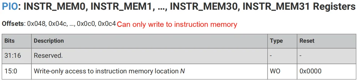
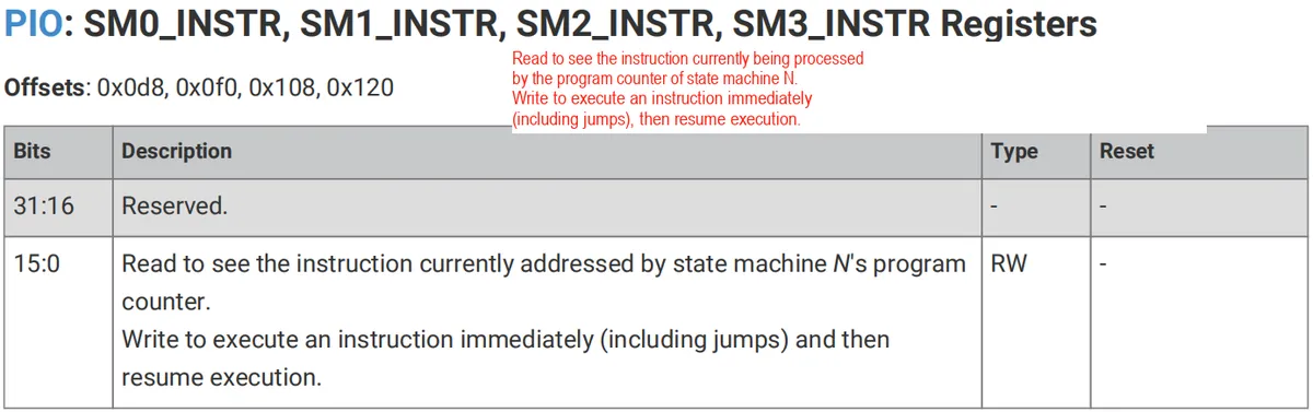
Write to the INSTR register: the delay cycles in the written instruction will be ignored and the instruction will be executed immediately, regardless of the setting of the clock divider of the finite-state machine. This interface is used to perform initialization or change process control, so the instruction will be executed as soon as possible regardless of the configuration of the finite-state machine.
Writing to INSTR with an instruction may enter a wait state, during which the finite-state machine will lock the instruction until it completes. When this occurs, the EXECCTRL_EXEC_STALLED flag will be set. Restarting the finite-state machine or writing INSTR with NOP can clear this flag.
The second stage of the PIO program for the finite-state machine in the above example uses the OUT EXEC instruction. OUT itself requires one execution cycle, and the instruction executed by OUT is carried out in the next execution cycle. Note that one of the instructions being executed is also OUT — the finite-state machine can only execute one OUT instruction per cycle.
OUT EXEC writes the data shifted out by OUT into the internal instruction register. In the next cycle, the finite-state machine knows that it should not execute the instruction memory, but instead execute the content of this latch, and also knows that it should not increment PC at this point.
Note that if an instruction written to INSTR causes a wait state, this instruction will be written to the same instruction register used by OUT EXEC and MOV EXEC, overwriting the instruction stored therein. Therefore, if the EXEC instruction is used, the instruction written to INSTR must not cause a wait state.
1.6 Registers Related to PIO Control on Raspberry Pi Pico
The base addresses of the PIO0 and PIO1 registers are 0x502000000 and 0x503000000 respectively.
We can perform operations such as resetting the clock division signal, resetting or enabling the finite-state machine, etc. , by reading from and writing to the CTRL control register:
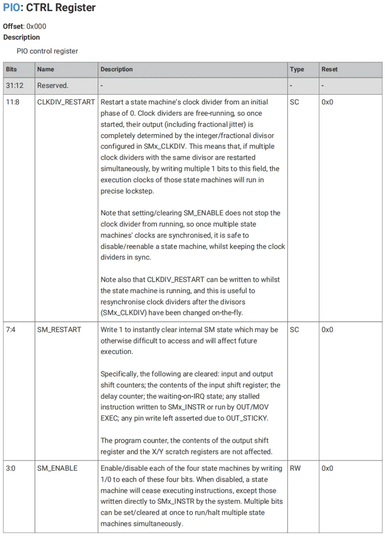
The FIFO status can be obtained by reading the FSTAT register:
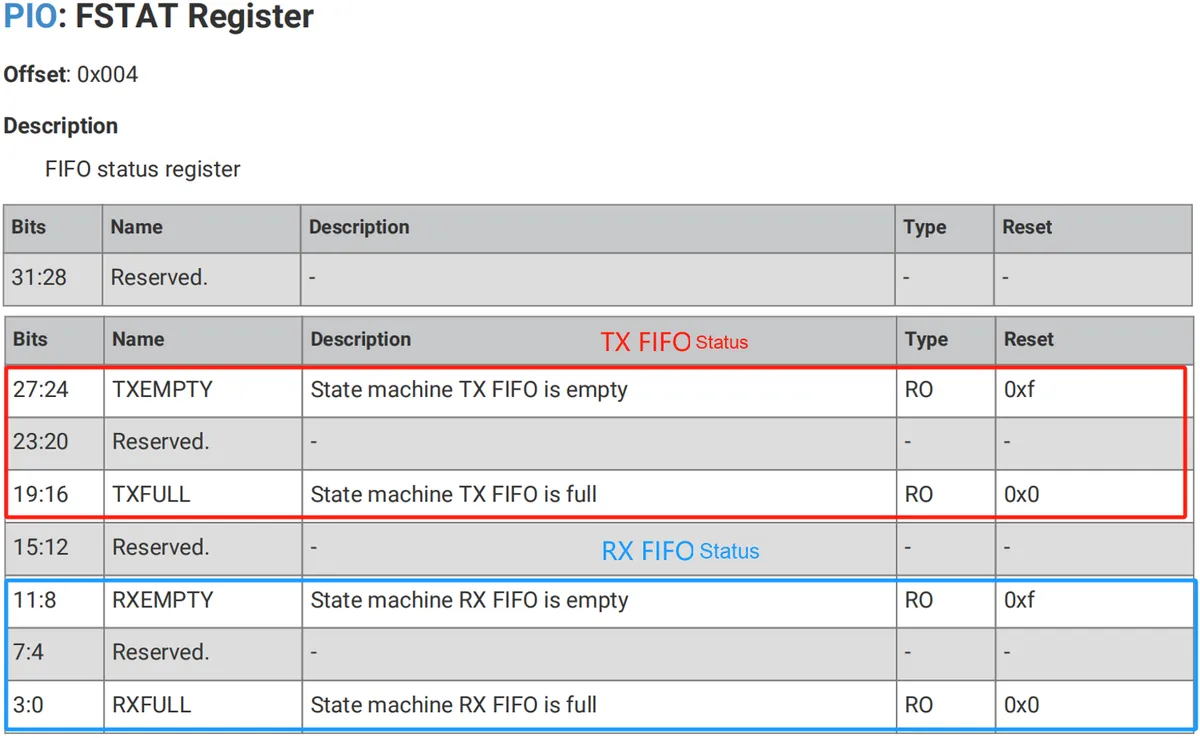
We can debug the FIFO by configuring the FDEBUG register to set the TX FIFO pause and overflow, as well as the RX FIFO empty read and pause:
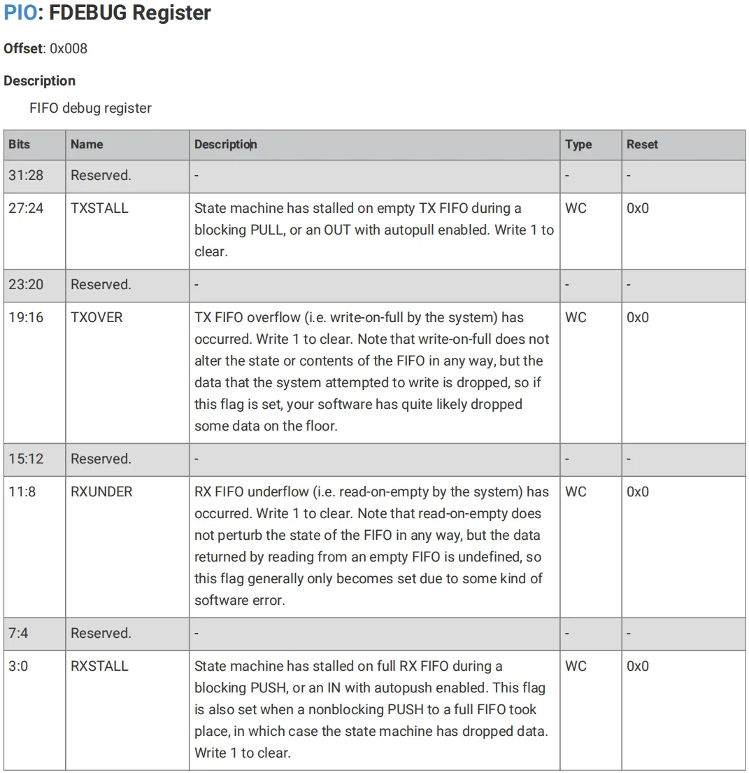
We can read the FIFO levels via the FLEVEL register:
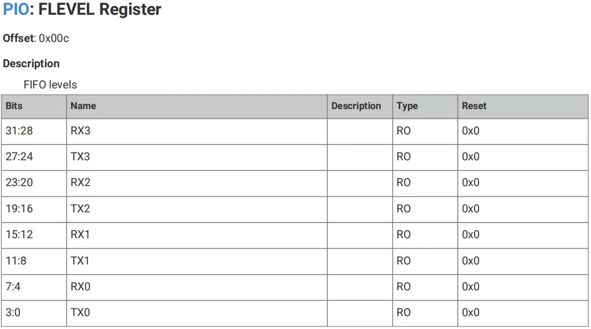
We can directly read and write the FIFO (x= 0~3) via the TXFx registers and RXFx registers:
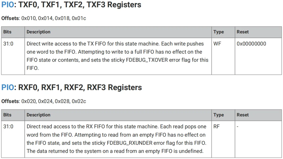
We can write 1 to the IRQ register to clear the interrupt flag bit of the finite-state machine:
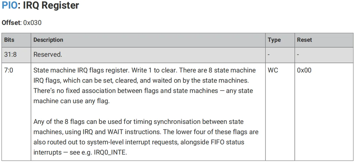
We can write 1 to the IRQ_FORCE register to forcefully assert the corresponding IRQ:
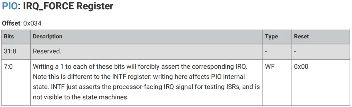
We can read the size of the instruction memory, the number of finite-state machines, and the depth of the TX/RX FIFOs by reading the DBG_CFGINFO register:
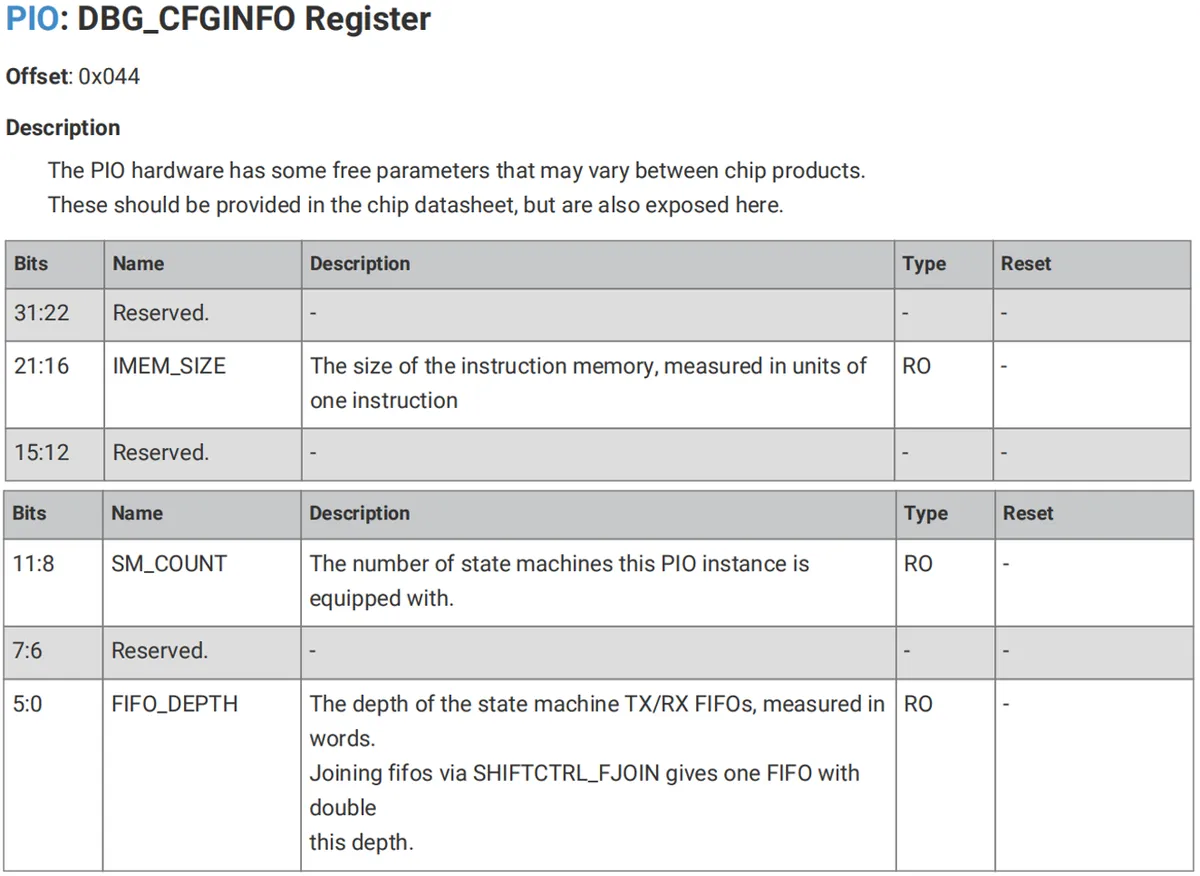
We can control the behavior of the finite-state machine via the EXECCTRL register, including enabling Side-set operations, jumping to Pin pins, WRAP folding-back, and other functions:
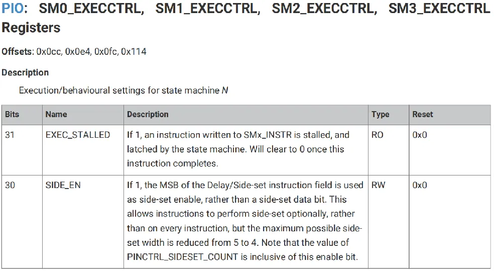
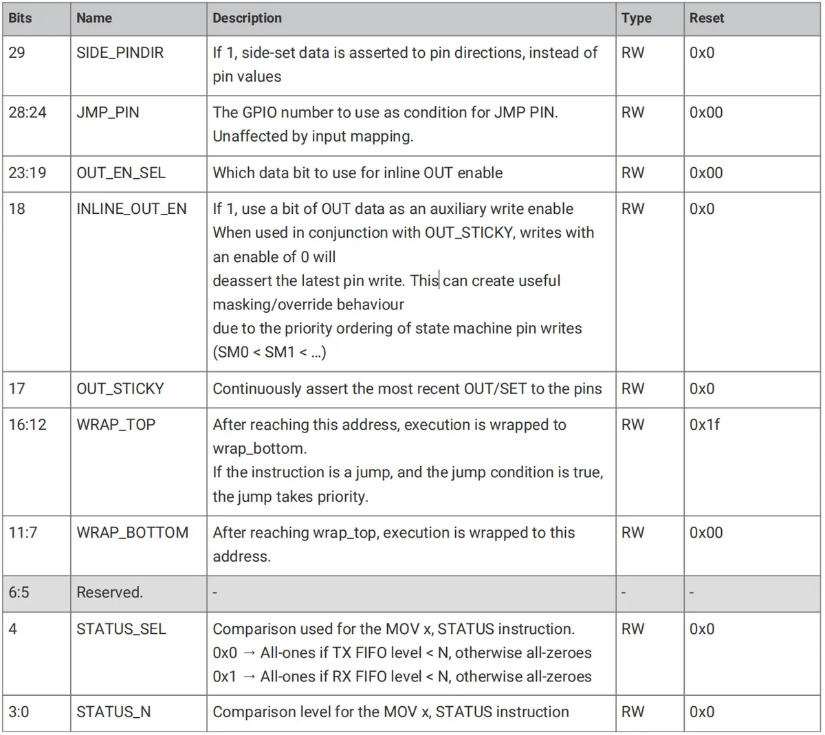
We can control the behavior of the OSR and ISR shifters via the SHIFTCTRL register, including operations such as FIFO merging, PUSH and PULL, and setting counter thresholds for auto-loading and auto-push:
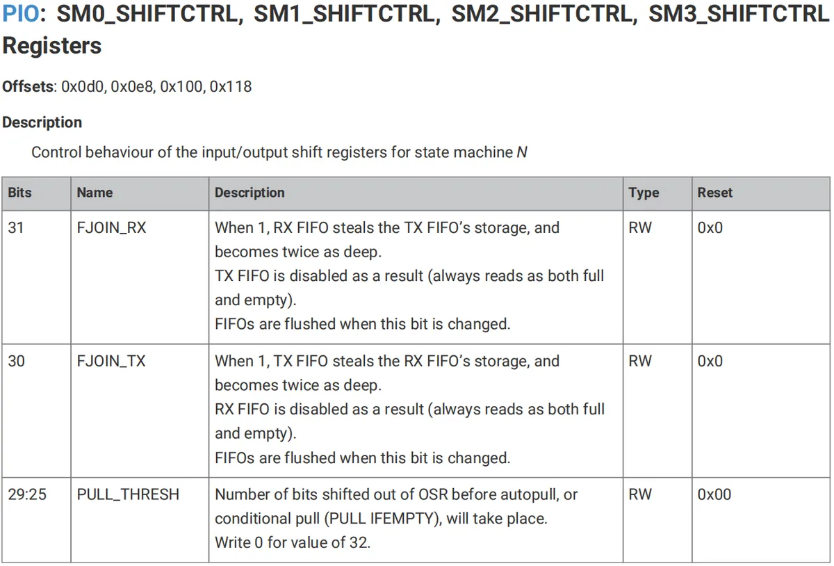
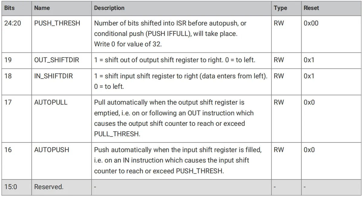
We can control pins via PINCTRL, including SET and OUT operation counting, as well as read/write operations on the pin base address for four types of operations:
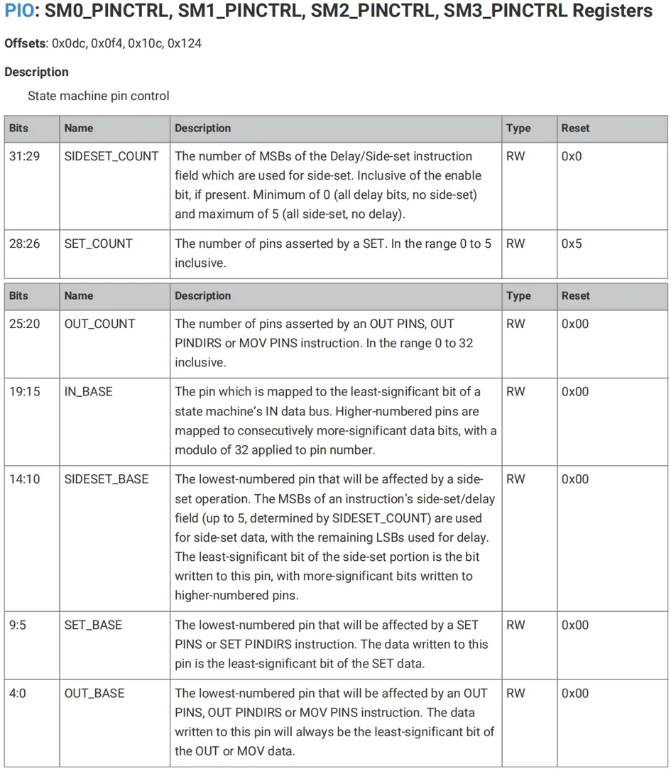
We have already explained the INSTR instruction register, CLKDIV frequency division register, INTE interrupt enable register, INTF interrupt force trigger register, INTR raw interrupt register and INTS masked interrupt register. Here we only explain some key registers in PIO control, and you can refer to the manual for the remaining registers by yourself.We will not go into detailed explanations of the additional principles and underlying mechanisms of PIO here. The focus of this content is on implementing different communication interfaces using PIO. Those who are interested can refer to the RP2040 datasheet and the Pico SDK development manual to learn more about the underlying principles of PIO.
2. Software Control Method
When controlling the PIO of Raspberry Pi Pico via MicroPython, it is necessary to use the @rp2.asm_pio decorator, as well as the PIO class and the StateMachine class:
- The pioasm assembler is written within the @rp2.asm_pio decorator function, and the GPIO pin mapping to be used, whether to enable automatic pull and automatic push, FIFO merging and other configurations are also specified in the rp2.asm_pio class.
- Configure a finite-state machine instance via the StateMachine class to run a given PIO program; meanwhile, the StateMachine class also provides control methods and status reading methods for the finite-state machine.
2.1 Constructor of the rp2.StateMachine Class
The constructor of the rp2.StateMachine class is as follows:
classrp2.StateMachine(id[, program, ...])
Construct a finite-state machine object with the given parameters.
The parameters are defined as follows:
- id - finite-state machine number. The RP2040 has two identical PIO instances, and each instance contains 4 finite-state machines: there are a total of 8 finite-state machines, numbered from 0 to 7
- program - you can choose to use a given program to initialize it
2.2 Other Methods of the rp2.StateMachine Class
The rp2.StateMachine class also features an initialization method, methods for setting or retrieving the running method, a restart method, and others:
Method | Description |
StateMachine.init (program, freq=-1, *, in_base=None, out_base=None, set_base=None, jmp_pin=None, sideset_base=None, in_shiftdir=None, out_shiftdir=None, push_thresh=None, pull_thresh=None) | Configure the finite-state machine instance to run the given program. This program is added to the instruction memory of this PIO instance. If the instruction memory already contains this program, its offset is reused to save on instruction memory space. The parameters are defined as follows:
|
StateMachine.active([value]) | Gets or sets whether the finite-state machine is currently running. The parameters are defined as follows:
|
StateMachine.restart() | Restart the finite-state machine and jump to the start of the program This method uses the SM_RESTART register of the RP2040 to clear the internal state of the finite-state machine, which includes:
|
StateMachine.exec(instr) | Execute a single PIO instruction. The parameters are defined as follows:
|
StateMachine.get(buf=None, shift=0) | Read one byte of data from the RX FIFO of the finite-state machine; if the FIFO is empty, it will block until data arrives. The parameters are defined as follows:
|
StateMachine.put(value, shift=0) | Write data to the TX FIFO of the finite-state machine. If the FIFO is full or becomes full, this method will block until the finite-state machine has transmitted enough words to complete the write operation. The parameters are defined as follows:
|
StateMachine.rx_fifo() | Returns the number of data bytes available in the RX FIFO of the finite-state machine; a value of 0 indicates that the FIFO is empty. It is very useful for checking whether data is waiting to be read before calling StateMachine.get (). |
StateMachine.tx_fifo() | Returns the number of data bytes available in the TX FIFO of the finite-state machine; a value of 0 indicates that the FIFO is empty. It is very useful for checking whether there is available space for data writing before calling StateMachine.put (). |
StateMachine.irq (handler=None, trigger=0 | 1, hard=False) | Returns the IRQ object for the given StateMachine, which can optionally be configured. |
2.3 Constructor Method of the rp2.PIO Class
The constructor of the rp2.PIO class is as follows:
class rp2.PIO(id)
Construct a PIO object with the given parameters.
The parameters are defined as follows:
- id - PIO peripheral number. The RP2040 has two identical PIO instances: PIO0 and PIO1
2.4 Other Methods of the rp2.PIO Class
Method | Description |
PIO.add_program(program) | Add the program to the instruction memory of this PIO instance. The amount of memory available for programs on each PIO instance is limited. If there is not enough space in the PIO's program memory, this method will raise an OSError (ENOMEM). |
PIO.remove_program([program]) | Delete the program from the instruction memory of this PIO instance. If no programs are provided, all programs will be deleted. Deleting an already deleted program will not trigger an error. |
PIO.state_machine(id[, program, ...]) | Obtain the finite-state machine number id. On the RP2040, each PIO instance has 4 finite-state machines, numbered 0 to 3. You can choose to use a program to initialize it.
|
PIO.irq (handler=None, trigger=IRQ_SM0 | IRQ_SM1 | IRQ_SM2 | IRQ_SM3, hard=False | Returns the IRQ object for this PIO instance. MicroPython only uses IRQ 0 on each PIO instance; IRQ 1 is not available. You can choose to configure it. |
2.5 Function for Assembling PIO Assembly Programs
There are three functions for assembling PIO assembly programs:
Method | Description |
rp2.asm_pio (*, out_init=None, set_init=None, sideset_init=None, in_shiftdir=0, out_shiftdir=0, autopush=False, autopull=False, push_thresh=32, pull_thresh=32, fifo_join=PIO.JOIN_NONE) | Assemble a PIO program. The parameters are defined as follows:
|
rp2.asm_pio_encode (instr, sideset_count, sideset_opt=False) | Assemble a single PIO instruction. The parameters are defined as follows: instr - Single PIO instruction sideset_count - Bit width for sideset operation sideset_opt - Whether to use the opt option |
rp2.bootsel_button() | Temporarily configure the QSPI_SS pin as an input and read its value; a return value of 1 indicates a low level, while 0 indicates a high level. On a typical RP2040 board with a BOOTSEL button, a return value of 1 indicates that the button is pressed. Since this function temporarily disables access to external flash memory, it also temporarily disables interrupts and other kernel components to prevent them from attempting to execute code from the flash. |
In addition, if an error occurs when assembling a PIO program, an rp2.PIOASMError will be raised from asm_pio () or asm_pio_encode (), and the class rp2.PIOASMError is an exception class dedicated to PIO.
2.6 PIO Instructions in MicroPython
In MicroPython, PIO assembly routines are written as Python functions decorated with @rp2.asm_pio () and they use Python syntax. Such routines support standard Python variables and arithmetic, as well as the following custom functions that encode PIO instructions and guide the assembler.
Instruction | Description |
wrap_target() | Specifies the position where the program resumes execution after a loop. By default, this is the start of the PIO routine. |
wrap() | Specifies the position where the program ends and returns. If this instruction is not used, it will be automatically added to the end of the PIO routine. Loopback does not consume any execution cycles. |
label(label) | Define a label named label at the current position. The label can be a string or an integer. |
word(instr, label=None) | Insert an arbitrary 16-bit word in the assembly output; the meaning of the parameters is as follows:
|
jmp(…) | This instruction has two forms:
|
wait(polarity, src, index) | Blocking delay, waiting for the high/low level on the pin or IRQ line.
|
in_(src, bit_count) | Move data from src to the ISR.
|
out(dest, bit_count) | Move the data out of the OSR to the target.
|
push(…) | Push the ISR into the RX FIFO, then clear the ISR. This instruction takes the following form:
If block is used, the instruction will block and pause when the RX FIFO is full. The default is block. If iffull is used, pushing will only occur when the input shift counter reaches its threshold. |
pull(…) | Pull OSR from TX FIFO. This instruction takes the following form:
If block is used, the instruction will stop when the TX FIFO is empty; the default setting is block. If ifempty is used, pulling is performed only when the output shift counter reaches its threshold. |
mov (dest, src) | Move the value from src to dest.
|
irq(…) | Set or clear the IRQ flag. This instruction has two forms:
If block is used, the instruction will stop until the flag is cleared by another object. If clear is used, the flag will be cleared instead of being set. The relative IRQ index is obtained by adding the finite-state machine ID to the IRQ index via modulo-4 addition. IRQ 0-3 are visible to the processor, while 4-7 are internal to the finite-state machine. |
set(dest, data) | Set dest using the value value.
|
nop() | This is a pseudo-instruction assembled as `mov (y, y)` and has no side effects. |
.side(value) | A modifier used to control the value of the side-set pins, which can be applied to any instruction.
|
.delay(value) | This is a modifier that can be applied to any instruction, and it is used to specify how many cycles to delay after the instruction is executed. value: delay cycle, ranging from 0 to 31 (the maximum value will be reduced if the side-set pins are used) |
[value] | This is a modifier, which is equivalent to. delay (value). |
3. Application Examples
3.1 Flashing the Onboard LED with PIO Control
The following code can be found in the material package we provide, in the elegance-devkit v1\Demo\29 PIO_LED folder.
We first use PIO to make the onboard LED of the Pico blink, and the sample code is as follows:
# Python env   : MicroPython v1.23.0
# -*- coding: utf-8 -*-
# @Time    : 2024/7/27 11:48 PM
# @Author  : Li Qingshui
# @File    : main.py
# @Description : Blink the onboard LED via PIO

# ======================================== Import Modules ========================================

# Import hardware-related modules
from machine import Pin
# Import time-related modules
import time
# Import RP2040-related modules
import rp2

# ======================================== Global Variables ============================================

# ======================================== Functions ============================================

# Define a PIO program that initializes the output pin to low level
@rp2.asm_pio(set_init=rp2.PIO.OUT_LOW)
def blink() -> None:
    """
    Define a PIO program that blinks an LED.

    Args:
        None

    Returns:
        None

    Description:
        This PIO program controls LED blinking by setting the pin high and low.
        The high level and low level each last 160 clock cycles, for a total period of 320 clock cycles.
    """
    # Mark the start of the program
    wrap_target()
    # Set the output pin high and delay for 31 clock cycles
    set(pins, 1)   [31]
    # The following nop instructions do nothing and delay for 31 clock cycles
    nop()          [31]
    nop()          [31]
    nop()          [31]
    nop()          [31]
    # Set the output pin low and delay for 31 clock cycles
    set(pins, 0)   [31]
    # The following nop instructions do nothing and delay for 31 clock cycles
    nop()          [31]
    nop()          [31]
    nop()          [31]
    nop()          [31]
    # The program jumps to wrap_target()
    wrap()

# ======================================== Custom Classes ============================================

# ======================================== Initialization ==========================================

# Power-on delay of 3 s
time.sleep(3)
# Print debug information
print("FreakStudio : Use PIO to control onboard LED")
# Create state machine 0, load the blink() program, set the PIO execution frequency to system clock/2000 Hz, and set the pin to pin 25
sm = rp2.StateMachine(0, blink, freq=2000, set_base=Pin(25))

# ========================================  Main Program  ===========================================

# Start state machine 0
sm.active(1)
# Delay 5 s
time.sleep(5)
# Stop state machine 0
sm.active(0)
Here, we mainly perform the following operations:
- Import modules: First, the necessary modules are imported, including machine for handling hardware operations, time for time-related tasks, and the rp2 module, which is a specific module in MicroPython for handling the dedicated functions of the Raspberry Pi Pico RP2040 chip.
- Function: This code defines a
blinkfunction, which is a PIO program used to control the blinking of an LED. This function uses the@rp2.asm_piodecorator to define the PIO program, and sets the initial state, frequency and pins of the program. - Initialization configuration: an object named
smof finite-state machine is created, which loads the previously definedblinkfunction, sets its frequency to 2000Hz, and assigns pin No. 25 to it. - Main Program: In the main program section, first start the finite-state machine
smto make it start executing theblinkfunction, so as to control the LED to blink. Then wait for 5 seconds, and finally shut down the finite-state machinesmto stop the LED from blinking.
Wherein, the blink function is a PIO program designed to toggle the state of the LED on each iteration. Specifically, it sets the output pin to a high level, holds it for a period of time (implemented via the nop instruction), then sets the pin to a low level and holds it for another period of time. This process repeats continuously, creating the blinking effect of the LED.
finite-state machine sm is responsible for executing the blink function. When the finite-state machine is activated (sm.active (1)), it will start executing the blink function; when the finite-state machine is deactivated (sm.active (0)), it will stop executing the blink function, and the configured frequency determines the blinking speed of the LED.
Here, the header and tail of the PIO program are as follows:
wrap_target()
...
wrap()  # The program jumps to wrap_target()
We can also use the label tag and the jmp instruction as an alternative:
label('loop')
...
jmp('loop') # The program jumps to loop
The difference between the two is that the jmp instruction takes one clock cycle to execute, while wrap consumes no time at all.
We use the set instruction to set the pin level:
set(pins, 1)  # High level
set(pins, 0)  # Low level
Here, `pins` is a name that pioasm automatically interprets, representing the pins to be written by the `set` instruction; we specify the base pin of `pins` via the `set_base` parameter of `rp2.StateMachine ()`(`pins` is a tuple of multiple pins, and `set_base` corresponds to the first element of `pins`), which is GPIO25.
Each complete blinking cycle consists of 320 clock cycles (160 clock cycles for the high level and 160 for the low level respectively), and the frequency of the finite-state machine is 2000 Hz, so each cycle takes 0.16 seconds, which corresponds to an LED blinking frequency of 6.25 Hz:
set (pins, 1)/set (pins, 0)Instruction: The instruction itself consumes 1 clock cycle, with a latency of 31 clock cycles, resulting in a total consumption of 32 clock cycles.nop ()Instruction: Each nop () consumes 1 clock cycle, plus an additional latency of 31 clock cycles, resulting in a total of 32 clock cycles per nop (); 4 consecutive nop () operations consume a total of 128 clock cycles.- High level part:
set (pins, 1)4 instances ofnop ()= 32 + 128 = 160 clock cycles. - Low-level portion:
set (pins, 0)4 instancesnop ()= 32 + 128 = 160 clock cycles.
The overall flow of the program is shown in the figure below:
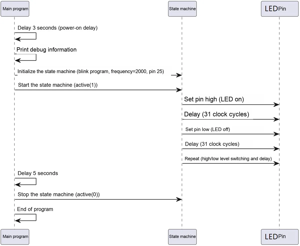
Burn the program into the Pico, and you will see the onboard LED on the Pico blink for 5 seconds and then stop blinking:
3.1 Application Experiment.mp4 17.2 MB
We modify the output pin to GP28, and the input command is as follows:
sm = rp2.StateMachine(0, blink, freq=2000, set_base=Pin(28))
sm.active(1)
Here, we use a logic analyzer to observe the output waveform, and it can be seen that the waveform frequency is indeed around the calculated value of 6.25 Hz:
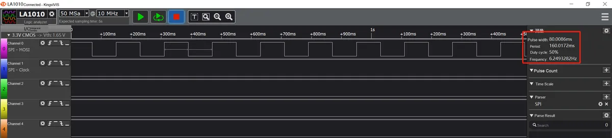
3.2 PIO Using Interrupts
Here, after we use the PIO program to trigger a finite-state machine interrupt via the irq instruction, we print the interrupt status flag of PIO in the main program: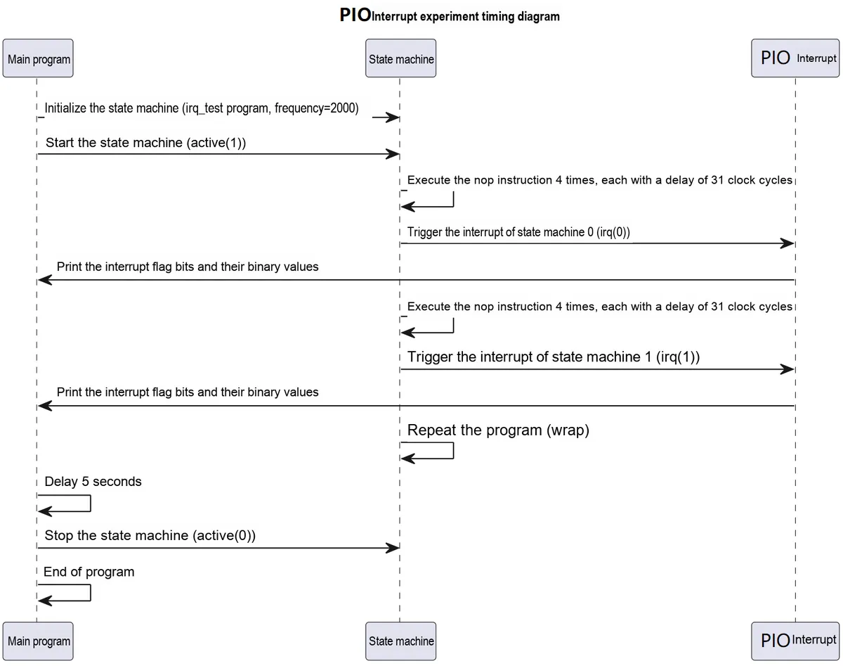
- In the
PIOprogram, use theirqinstruction to trigger an interrupt for the finite-state machine - Configure
the interrupt handler for PIO0to print the interrupt flag bit and its corresponding binary value when an interrupt occurs. - Create a finite-state machine, set
irq_test ()as the program, and configure the frequency to1/2000of the system clock in Hz - Start the finite-state machine and turn it off after a 5-second delay
The following code can be found in the elegance-devkit v1\Demo\30 PIO_IRQ folder of the resource package we provide.
The sample code is as follows:
# Python env   : MicroPython v1.23.0
# -*- coding: utf-8 -*-
# @Time    : 2024/7/28 10:32 AM
# @Author  : Li Qingshui
# @File    : main.py
# @Description : PIO experiment: use the irq instruction in a PIO program to trigger an interrupt and print the interrupt flags

# ======================================== Import Modules ========================================

# Import time-related modules
import time
# Import RP2040-related modules
import rp2

# ======================================== Global Variables ============================================

# ======================================== Functions ============================================

# The irq_test() function defines a PIO (Programmable I/O) program using the rp2.asm_pio() decorator
@rp2.asm_pio()
def irq_test() -> None:
    """
    Define a PIO program for testing interrupts.

    Args:
        None

    Returns:
        None

    Description:
        This PIO program tests the interrupt function by executing nop instructions and triggering interrupts.
        The program triggers the interrupts of state machine 0 and state machine 1 in turn, and inserts a delay after each interrupt.
    """
    # Marks the start of the program
    wrap_target()
    # 4 nop() no-operation instructions, each with a delay of 31 clock cycles
    nop()          [31]
    nop()          [31]
    nop()          [31]
    nop()          [31]
    # Trigger the interrupt of state machine 0
    irq(0)
    # 4 nop() no-operation instructions, each with a delay of 31 clock cycles
    nop()          [31]
    nop()          [31]
    nop()          [31]
    nop()          [31]
    # Trigger the interrupt of state machine 1
    irq(1)
    # Marks the end of the program and returns to the start
    wrap()

# Convert to binary data with a fixed number of bits
def to_bin(value: int, num: int) -> str:
    """
    Convert a decimal number to a binary number with a fixed number of bits.

    Args:
        value (int): The decimal number to convert.
        num (int): The fixed number of bits of the binary number.

    Returns:
        str: The converted binary string.
    """
    # Initialize an empty string bin_chars to store the final binary data
    bin_chars = ""
    # Save the original decimal number value to a temporary variable temp
    temp = value
    # Loop num times
    for i in range(num):
        # Get the remainder of temp divided by 2, i.e. the last bit of the binary number, convert it to a string, and assign it to bin_char
        bin_char = bin(temp % 2)[-1]
        # Divide temp by 2 (integer division) and assign the new value to temp
        temp = temp // 2
        # Prepend bin_char to bin_chars to build the correct binary bit order
        bin_chars = bin_char + bin_chars
    # Return the converted binary string bin_chars, converted to uppercase
    return bin_chars.upper()

# ======================================== Custom Classes ============================================

# ======================================== Initialization ==========================================

# Power-on delay of 3 s
time.sleep(3)
# Print debug information
print("FreakStudio: PIO IRQ Test")

# Set a lambda function as the interrupt handler of PIO 0. When an IRQ occurs, the function prints the interrupt flags and the corresponding binary number (12 bits wide)
rp2.PIO(0).irq(lambda pio: print(pio.irq().flags(),to_bin(pio.irq().flags(),12)))
# Create a state machine, use the irq_test() function as the program, and set the frequency to system clock/2000 Hz
sm = rp2.StateMachine(0, irq_test, freq=2000)

# ========================================  Main Program  ===========================================

# Start the state machine
sm.active(1)
# Wait 5 seconds
time.sleep(5)
# Stop the state machine
sm.active(0)
Here, in the PIO0 interrupt handler section:
# Set a lambda function as the interrupt handler of PIO 0. When an IRQ occurs, the function prints the interrupt flags and the corresponding binary number (12 bits wide)
rp2.PIO(0).irq(lambda pio: print(pio.irq().flags(),to_bin(pio.irq().flags(),12)))
Here, pio is the parameter of the lambda function, representing the incoming PIO instance, followed by the expression part:
pio.irq ()gets the interrupt object of the current PIO.. flags ()is a method of this interrupt object, which returns the current interrupt flag bits;to_bin ()is a custom function used to convert an integer into a fixed-length binary string
That is, each interrupt will print the decimal value of the interrupt flag bit and the 12-bit binary string of the interrupt flag bit.
After flashing the code to Pico, the remote connection was interrupted, and the data output is as follows:
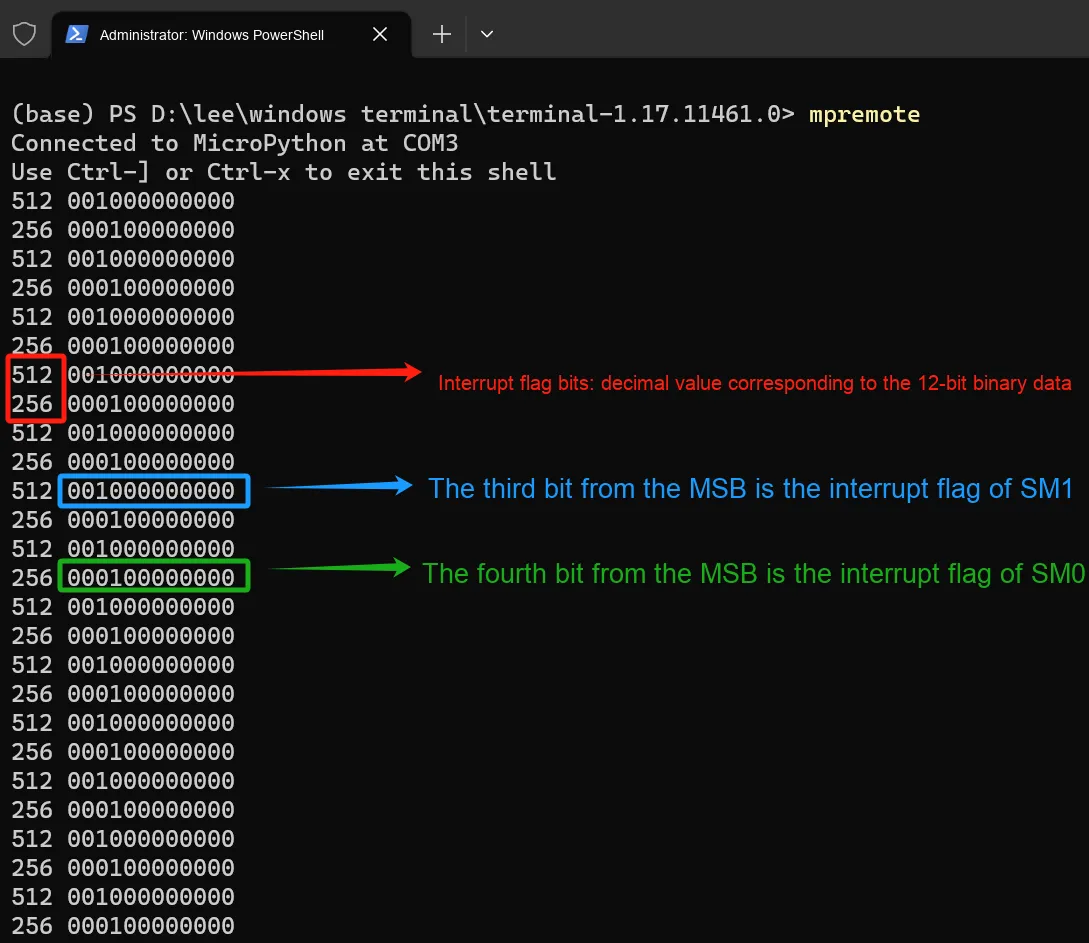
3.2 Application Experiment.mp4 4.5 MB
Let's take a look at PIO0 's interrupt mask output register:
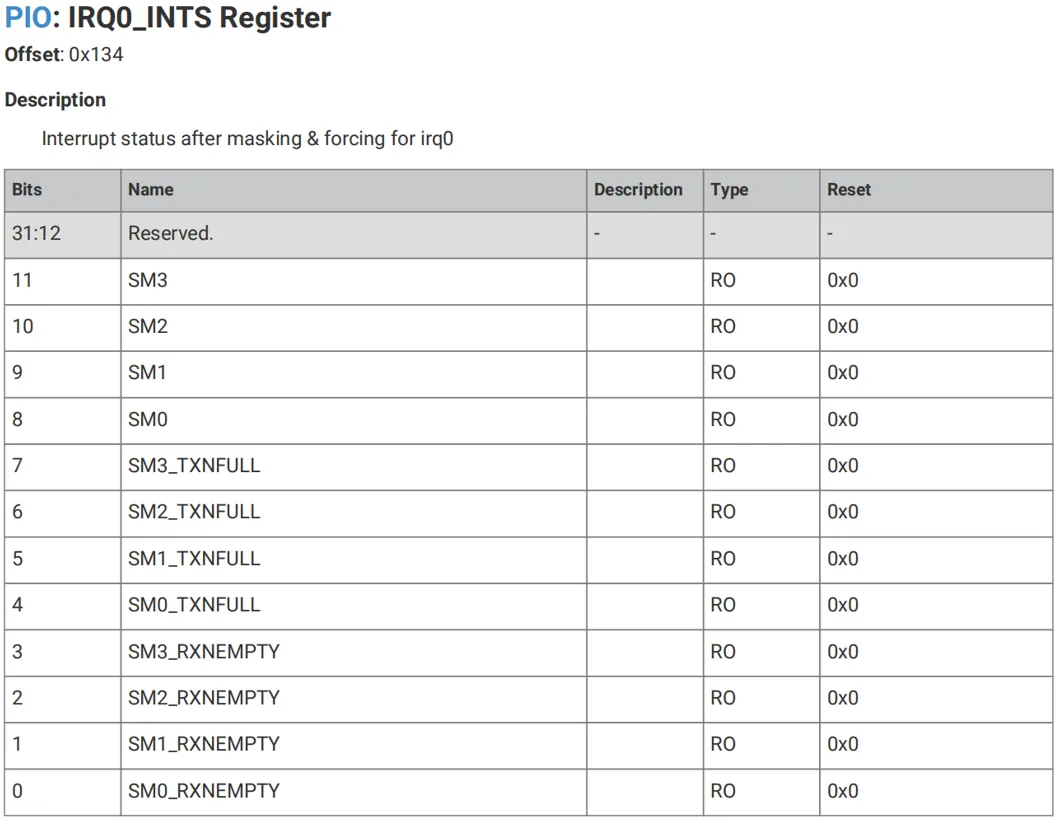
It can be seen that:
- The binary data corresponding to 512 is
0b001000000000, which indicates thatSM1generates an interrupt - The binary data corresponding to 256 is
0b000100000000, which indicates thatSM0generates an interrupt
3.3 PIO uses exec to execute instructions in the instr register
As we mentioned earlier, in addition to the instruction memory, the finite-state machine can also execute instructions from three other sources:
MOV EXECcan execute instructions from a register specified bySource.OUT EXECcan execute the data migrated by OSR.- Execute instructions from the
SMx_INSTRcontrol register; the system can write instructions directly to this register for immediate execution.
Next, we use the StateMachine.exec () method to encode the instructions from the given string instr.
The following code can be found in the material package we provide, at the elegance-devkit v1\Demo\31 PIO_Exec folder.
The sample code is as follows:
# Python env   : MicroPython v1.23.0
# -*- coding: utf-8 -*-
# @Time    : 2024/7/28 11:16 AM
# @Author  : Li Qingshui
# @File    : main.py
# @Description : PIO experiment: use the exec instruction in a PIO program to execute pioasm instructions

# ======================================== Import Modules ========================================

# Import time-related modules
import time
# Import RP2040-related modules
import rp2
# Import hardware-related modules
from machine import Pin

# ======================================== Global Variables ============================================

# ======================================== Functions ============================================

# Define a PIO program with a decorator: the blink function, which does nothing
@rp2.asm_pio(set_init=rp2.PIO.OUT_LOW)
def blink() -> None:
    """
    Define an empty PIO program.

    Args:
        None

    Returns:
        None

    Description:
        This PIO program does nothing and serves only as a placeholder program for the state machine.
    """
    pass

# ======================================== Custom Classes ============================================

# ======================================== Initialization ==========================================

# Power-on delay of 3 s
time.sleep(3)
# Print debug information
print("FreakStudio: PIO use exec instruction to execute pioasm instruction")

# Create a state machine, use the blink() function as the program, set the frequency to system clock/2000 Hz, and set set_bases to GPIO25
sm = rp2.StateMachine(0, blink, freq=2000, set_base=Pin(25))

# ========================================  Main Program  ===========================================

# Start the state machine
sm.active(1)

while True:
    # The state machine loads the instruction 'set(pins, 1)'
    sm.exec('set(pins, 1)')
    # Delay 1s
    time.sleep(1)
    # The state machine loads the instruction 'set(pins, 0)'
    sm.exec('set(pins, 0)')
    # Delay 1s
    time.sleep(1)
The overall execution process is shown in the following figure:
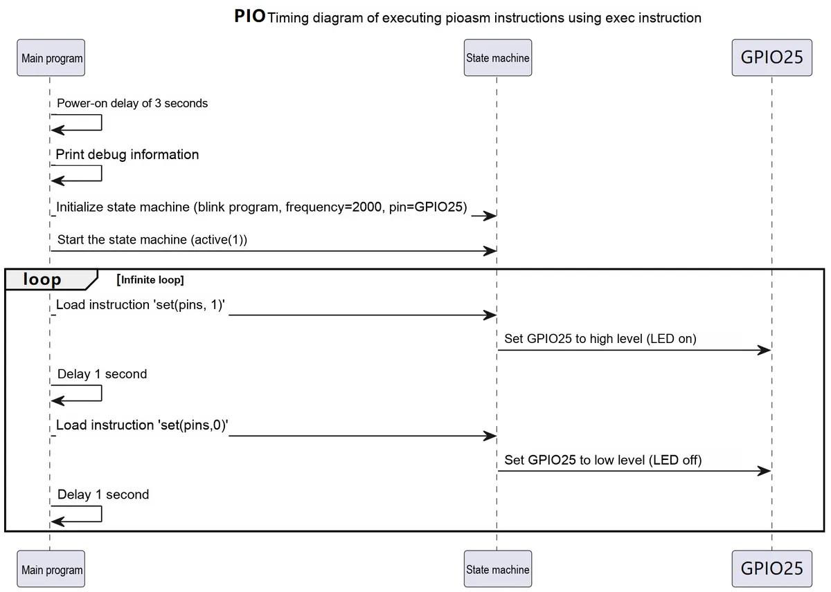
Burn the code to Pico, and you will see the on-board LED blinking:
3.3 Application Experiment.mp4 18.5 MB
3.4 PIO Control of WS2182 Colorful Lights
3.4.1 Introduction to WS2812 LED
WS2812 LED is a type of individually addressable RGB LED under the Neopixel series, and we can control multiple WS2812 RGB tricolor LEDs via a single data line. The working principle of WS2812 is to transmit 24-bit RGB color data to each LED bead one by one through a single data line. Each WS2812 chip is equipped with a shift register for receiving and forwarding data. Once a complete frame of RGB data is received, the corresponding LED bead will display the matching color.By connecting multiple WS2812 lamp beads in series, flexible and programmable LED strips, LED matrices and other components can be formed. Common applications include decorative lighting, LED displays, smart lamps and the like.
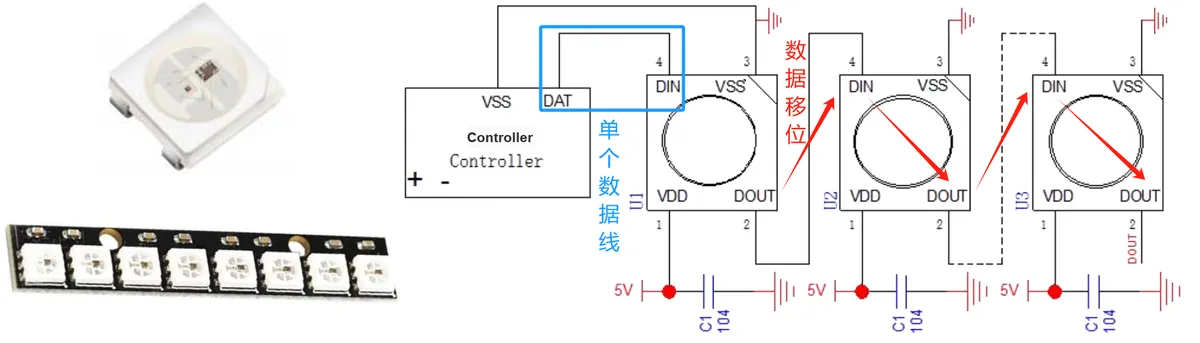
The main features of the WS2812 include:
- High integration: A single WS2812 LED integrates RGB tri-color LEDs and a control chip inside, and can be controlled with only a single data line.
- Series control: Multiple WS2812 LED beads can be used in series to form an LED strip or an LED array.
- Programmable control: By programming to control data signals, independent dimming and color control for each LED can be realized.
- Low power consumption: The operating voltage is 5V, and the power consumption of a single LED is only 60mW
- High Brightness: LEDs feature high luminous brightness, with the maximum brightness reaching 6500~8000 mcd
- Compact size: The package measures only 5.0mm x 5.0mm x 1.6mm
WS2812 has four pins, and their functions are as follows:
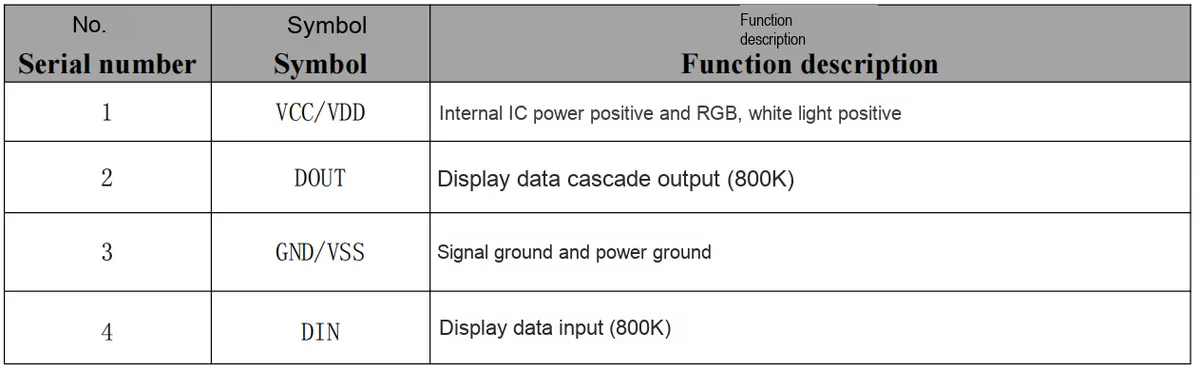
It adopts the communication mode of unipolar return-to-zero code, and each symbol must have a low level:
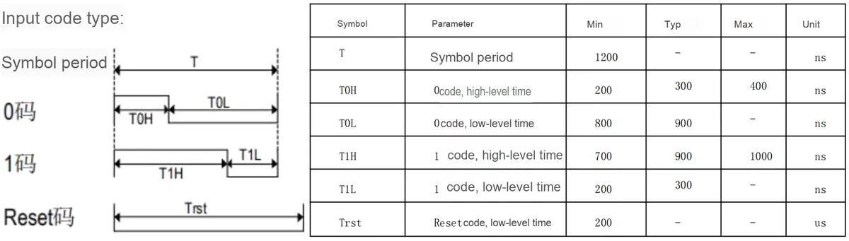
Unipolar Return-to-Zero Code
Unipolar return-to-zero code refers to a coding scheme where high level and zero level represent binary 1 and 0 respectively: "0" is represented by no voltage, while "1" is represented by a constant positive voltage whose duration is shorter than the time width of one symbol, that is, a narrow pulse is transmitted. The sampling time is set at the midpoint of each symbol period, and the decision threshold is set at half the amplitude level.
It has the following features:
- Unipolar: The signal has only two states, high level (1) and low level (0), with no negative level.
- Return-to-zero: Between each symbol, there will always be a low-level state, which is referred to as "return-to-zero"
- Symbol time: The time length of each symbol is equal.
- Symbol value: Each symbol is either at a high level or a low level
The encoding rules of unipolar return-to-zero code are as follows:
- When encoding "1", a high level is output to occupy the entire symbol duration
- When encoding "0", the output is a low level that occupies the entire symbol duration.
- There is a low-level period (return-to-zero interval) between every two symbols.
You can refer to the following link for the Sequence Diagram of its encoding method:
https://en.wikipedia.org/wiki/File:Digital_signal_encoding_formats-en.svg
After the chip is powered on and reset, DIN pin receives the data transmitted from the controller:
- First, the incoming 24-bit data is extracted by the first chip and then sent to the data latch inside the chip.
- The data latch inside the chip generates duty cycle control signals with different duty ratios at the OUTR, OUTG and OUTB control terminals according to the received 24-bit data, so that the LED produces different colors.
- The remaining data, after being shaped and amplified by the internal shaping processing circuit, starts to be forwarded and input to the next cascaded chip via the DO port; with each transmission through a chip, the signal is reduced by 24 bits.
- When the chip does not receive the RESET signal input from the DIN terminal, the output of the OUTR, OUTG and OUTB pins remains unchanged; after receiving the RESET signal, each control terminal will change its output according to the received data.
The chip adopts automatic shaping and forwarding technology, so that the number of cascades of the chip is not limited by signal transmission, but only restricted by the requirements of signal transmission speed.
Its Communication Protocol is: reset signal + 24-bit data of the first chip + 24-bit data of the second chip +. .. + 24-bit data of the Nth chip. The highest bit is transmitted first, in the order of GRB (different WS2812 chips have different color orders, please refer to the datasheet):

Among them, bits R0-R7 control the red light color output, bits G0-G7 control the green light color output, and bits B0-B7 control the blue light color output. Since each LED bead needs to store 24-bit RGB color data, when the light strip is long and there are a large number of LED beads, the video memory data will occupy a large amount of RAM space.
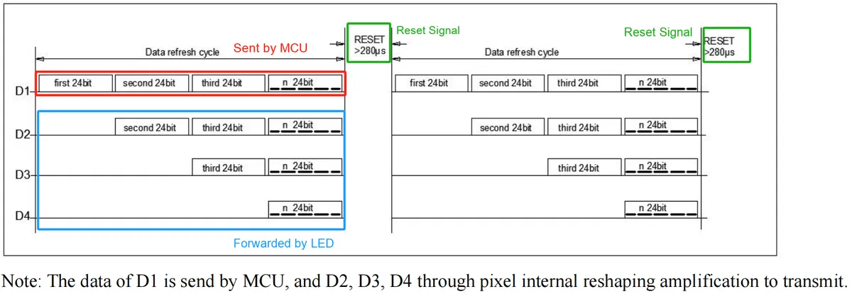
Wherein D1 is the data sent by the MCU terminal, and D2, D3, D4 are the data automatically shaped and forwarded by the cascade circuit. The controller can continuously send 24-bit RGB control signals; after the first LED bead intercepts the first 24 bits of data, it displays the data on its own LED, shapes the remaining data and then sends it to the second LED bead. The second LED bead will intercept the second set of 24-bit data for display, and continue to forward the remaining data until the last set of data is displayed.
The electrical parameters of WS2812 are as follows:
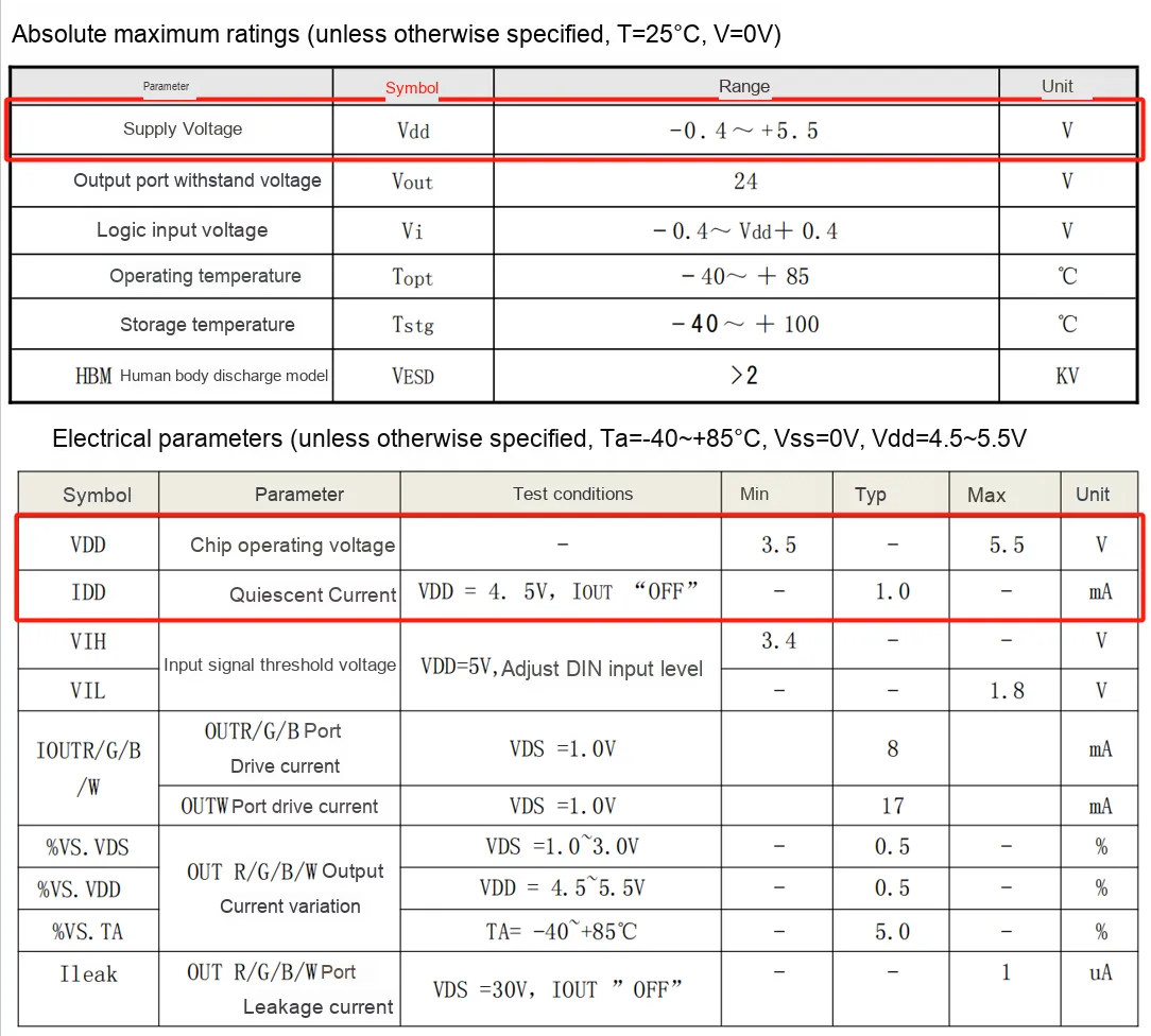
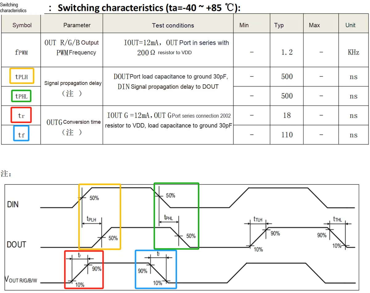
3.4.2 Driving WS2812 LEDs with the NeoPixel Class
We can use the built-in neopixel module in the MicroPython library, specifically the NeoPixel class, to drive WS2812 LED lights:
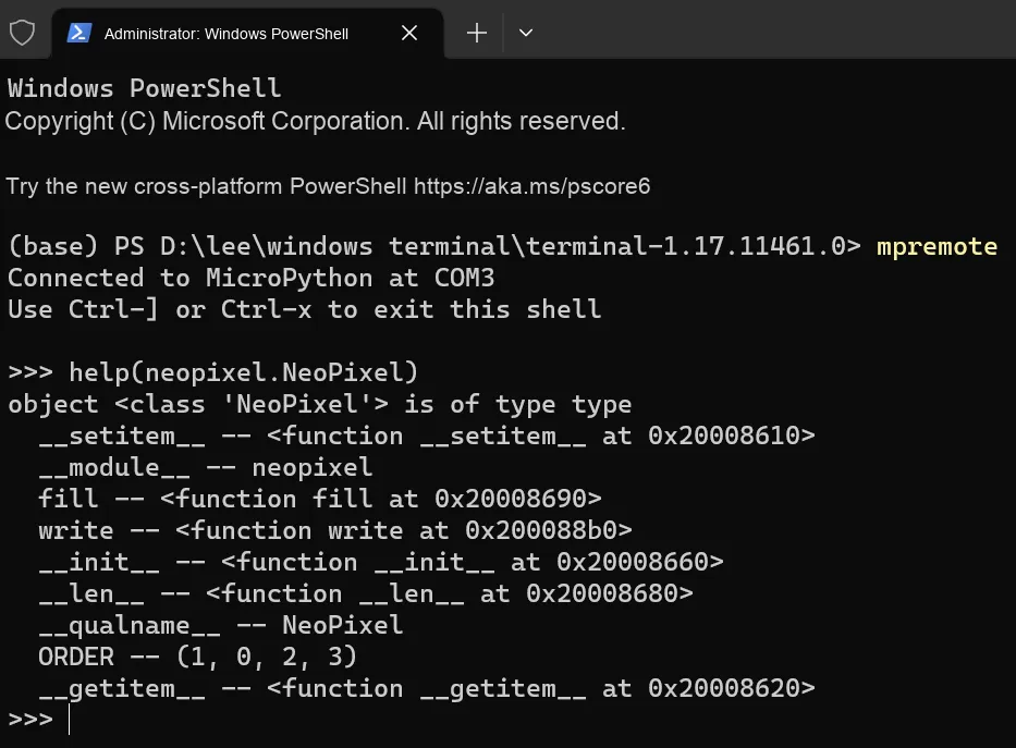
It provides the following methods to control WS2812 LED lights:
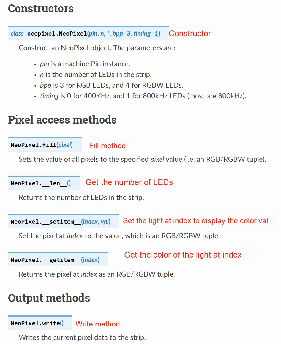
RGB Lights and RGBW Lights
Here, the WS2812 LEDs are also divided into two types: RGBW LEDs and RGB LEDs. There are some differences between them:
- LED bead composition:
- RGB lamp beads consist of three LEDs in red (R), green (G) and blue (B).
- The RGBW LED bead additionally incorporates a white (W) LED, offering a total of 4 colors.
- Color Gamut Coverage:
- RGB lights can only generate other colors by mixing the three primary colors, featuring a small color gamut that fails to cover some warm and vivid colors.
- RGBW lights, with the added white channel, can produce richer colors and feature a wider color gamut, offering particular advantages when generating warm color tones and high brightness.
- Brightness Performance:
- RGB lights require the mixing of three-color LEDs to produce white light, which leads to a certain degree of attenuation.
- RGBW lights can directly use white LEDs to generate white light, delivering higher brightness and better efficiency.
- Communication Method:
- RGB lights usually transmit 24-bit data and use 3 separate channels to control the three primary colors
- RGBW lights require 32-bit data and use 4 independent channels to control the four colors R, G, B and W respectively
In the following experiment, we need to insert the Fengya No. 1 Board - Colorful Touch Expansion Board into the Fengya No. 1 Board - Universal Compatible Expansion Board, and meanwhile turn on the SWITCH2 DIP switch's WS2812 option:
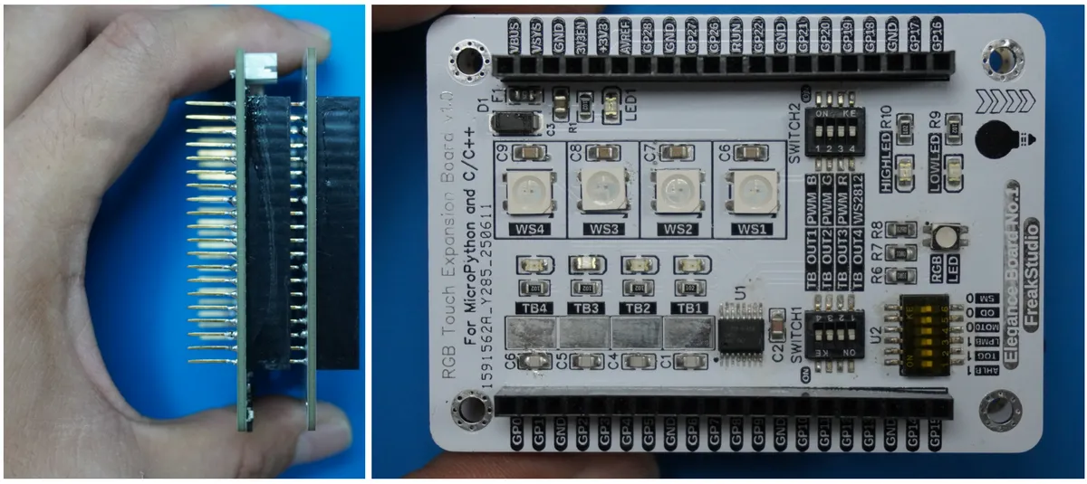
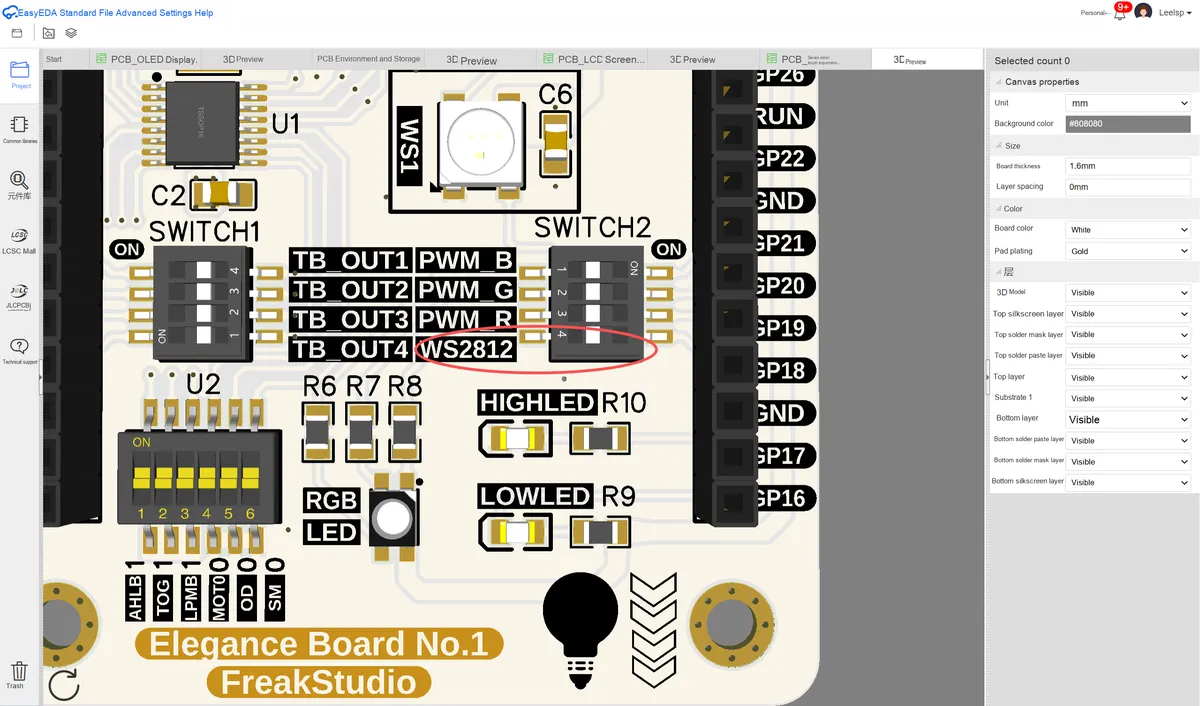
In the following code, we use a single row of 4 WS2812 to implement a flowing LED light, and use the GP18 pin of the Raspberry Pi Pico as the signal line for the WS2812. The WS2812 LEDs are powered by 5V. The following code can be found in the elegance-devkit v1\Demo\32 NeoPixel folder in the resource package we provided.
The basic working principle is: the light-on function is called periodically, and in the light-on function, all LED lights are traversed, the currently selected light is set to red, and the other lights are set to blue. Then it updates the NeoPixel strip to display the new color. After each light is polling to display red once, all of them turn green, and then the cycle repeats.
The sample code is as follows:
# Python env   : MicroPython v1.23.0
# -*- coding: utf-8 -*-
# @Time    : 2024/7/27 2:55 PM
# @Author  : Li Qingshui
# @File    : main.py
# @Description : Blink a NeoPixel strip via GPIO

# ======================================== Import Modules ========================================

# Import hardware-related modules
from machine import Pin, Timer
# Import time-related modules
import time
# Import NeoPixel-related modules
from neopixel import NeoPixel
# Import the random number module
import random

# ======================================== Global Variables ============================================

# Define the GPIO pin the NeoPixel is connected to as 18
NEOPIXEL_PIN = 18
# Define the number of LEDs on the NeoPixel strip as 4
NUMBER_PIXELS = 4
# Define a counter variable to control LED movement
counter = 0

# ======================================== Functions ============================================

def move_pixel(timer: Timer) -> None:
    """
    Move the LED on the NeoPixel strip.

    Args:
        timer (machine.Timer): Timer instance.

    Returns:
        None

    Description:
        This function is called periodically by a timer to control the LED movement on the NeoPixel strip.
        The current LED shows red and the other LEDs show blue. When the counter exceeds the number of LEDs, all LEDs show green and the counter is reset.
    """
    # Declare the counter variable as global so that it can be modified inside the function
    global counter

    # Iterate over all NeoPixel LEDs
    for i in range(0, NUMBER_PIXELS):
        # If the index of the current LED equals the counter value, set it to red (10,0,0)
        if i == counter:
            strip[i] = (55,0,0)
        # Otherwise, set it to blue (0,0,10)
        else:
            strip[i] = (0,0,55)
        # Write the updated colors to the NeoPixel strip
        strip.write()

    # Increment the counter variable to control the movement of the next LED
    counter += 1

    # If counter is greater than the number of LEDs
    if counter > NUMBER_PIXELS:
        # Set all LEDs to green (0,10,0)
        strip.fill((0,55,0))
        strip.write()
        # Reset counter to 0
        counter = 0

def random_color_flow(timer: Timer) -> None:
    """
    Implement a random-color chasing light effect.

    Args:
        timer (machine.Timer): Timer instance.

    Returns:
        None

    Description:
        This function is called periodically by a timer to make the LEDs on the NeoPixel strip display random colors.
        Each time it is called, the colors of all LEDs are updated to random colors.
    """
    # Declare the counter variable as global so that it can be modified inside the function
    global counter

    # Iterate over all NeoPixel LEDs
    for i in range(NUMBER_PIXELS):
        # Set a random color (R, G, B) for each LED
        strip[i] = (random.randint(0, 55), random.randint(0, 55), random.randint(0, 55))

    # Write the updated colors to the NeoPixel strip
    strip.write()

# ======================================== Custom Classes ============================================

# ======================================== Initialization ==========================================

# Power-on delay of 3 s
time.sleep(3)
# Print debug information
print("FreakStudio: Using NeoPixel to control WS2812 LED")

# Create a NeoPixel object connected to GPIO pin 18, with the number of LEDs set to 4
strip = NeoPixel(Pin(NEOPIXEL_PIN), NUMBER_PIXELS)
# Create a software timer object
timer = Timer(-1)

# ========================================  Main Program  ===========================================

# Initialize the timer to trigger the move_pixel function every 200 ms
timer.init(period=200, mode=Timer.PERIODIC, callback=random_color_flow)

while True:
    # Print the current counter value
    print('timer counter :', counter)
    # Delay 5 s
    time.sleep(5)
Its workflow is shown in the following figure:
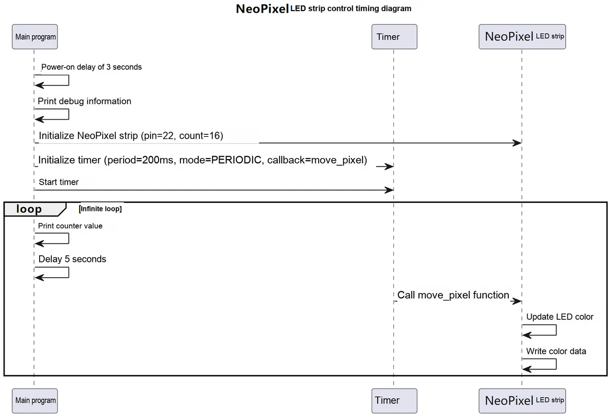
Burn the code to the Pico and connect to the remote terminal, you will see that the WS2812 chasing LED light has been implemented:
3.4.1 Application Experiment.mp4 11.5 MB
And the terminal outputs the count value at regular intervals:
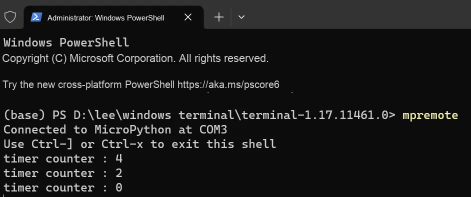
We can also modify the timer callback function to the random_color_flow () function to implement arbitrary flowing light effects:
# Initialize the timer to trigger the move_pixel function every 200 ms
timer.init(period=200, mode=Timer.PERIODIC, callback=random_color_flow)
The basic principle is to use the random library built into MicroPython, and the randint function in it to generate a random RGB color array. After flashing the code, the effect is shown in the following figure:
3.4.3 Application Experiment.mp4 15.5 MB
3.4.3 Using PIO to Drive WS2812 LEDs
Using PIO to control WS2812 color lights, compared with using the built-in neopixel module to control WS2812 color lights, has the advantage of high real-time performance: PIO is a dedicated hardware peripheral that can run independently of the CPU, perform specific data transmission tasks, and generate precise timing signals without CPU involvement, thus greatly reducing the load on the CPU. This hardware acceleration method can achieve higher transmission efficiency and lower power consumption.
In the following experiment, we need to insert the Fengya No. 1 Board - Colorful Touch Expansion Board into the Fengya No. 1 Board - Universal Compatible Expansion Board, and meanwhile turn on the SWITCH2 DIP switch's WS2812 option:
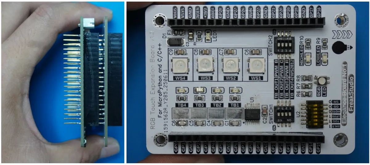
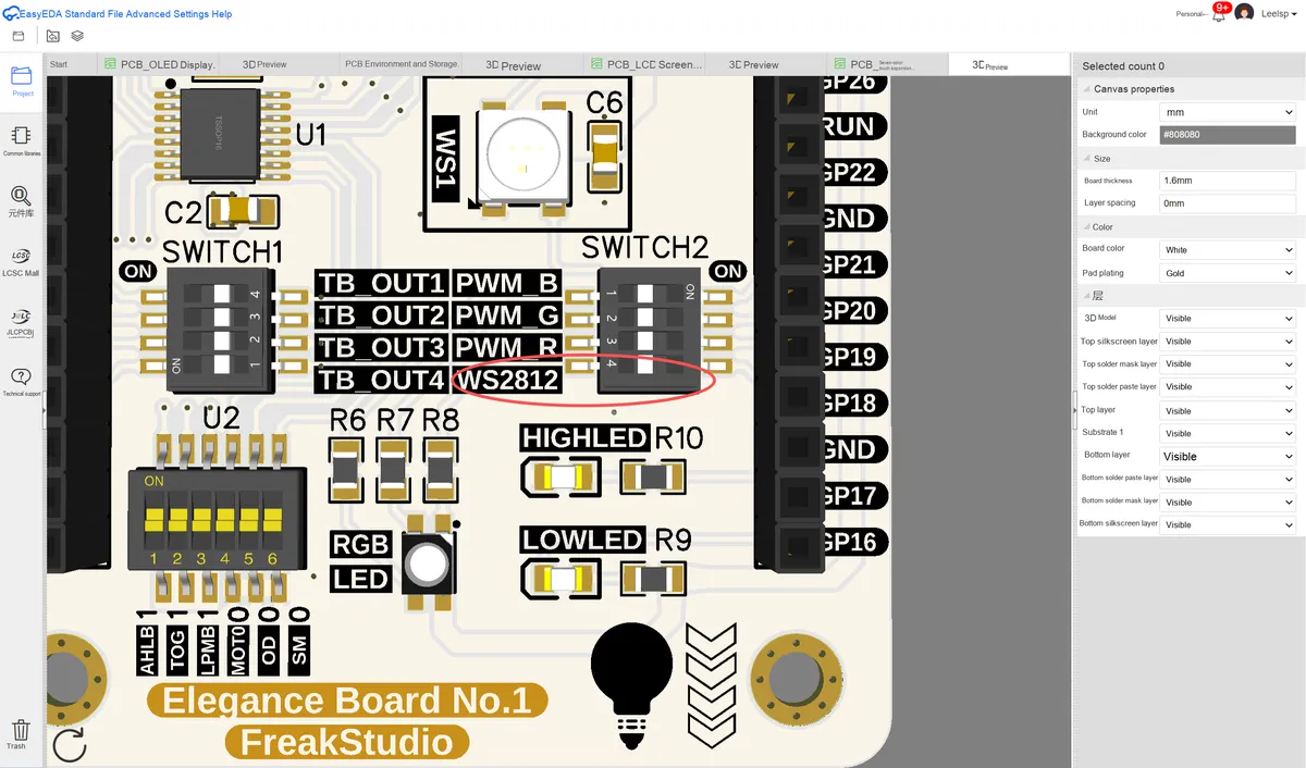
The following code can be found in the material package we provide, under the elegance-devkit v1\Demo\33 PIO_NeoPixel folder.
Next, let's take a look at how to use PIO finite-state machine to control NeoPixel to implement a colorful flowing LED light, the sample code is as follows:
# Python env   : MicroPython v1.23.0
# -*- coding: utf-8 -*-
# @Time    : 2024/7/27 9:52 PM
# @Author  : Li Qingshui
# @File    : main.py
# @Description : Blink a NeoPixel strip via PIO

# ======================================== Import Modules ========================================

# Import hardware-related modules
from machine import Pin
# Import time-related modules
import time
# Import RP2040-related modules
import rp2

# ======================================== Global Variables ============================================

# Color list of the LED strip
colors = [
    (128, 0, 0),    # LED 1, red, reduced brightness
    (128, 82, 0),   # LED 2, orange, reduced brightness
    (128, 128, 0),  # LED 3, yellow, reduced brightness
    (0, 128, 0),    # LED 4, green, reduced brightness
    (0, 128, 128),  # LED 5, cyan, reduced brightness
    (0, 0, 128),    # LED 6, blue, reduced brightness
    (38, 0, 65),    # LED 7, purple, reduced brightness
    (119, 65, 119), # LED 8, violet, reduced brightness
    (128, 53, 90),  # LED 9, hot pink, reduced brightness
    (128, 10, 74),  # LED 10, deep pink, reduced brightness
    (128, 128, 128),# LED 11, white, reduced brightness
    (96, 96, 96),   # LED 12, silver, reduced brightness
    (0, 0, 0),      # LED 13, black
    (64, 64, 64),   # LED 14, gray, reduced brightness
    (128, 0, 128),  # LED 15, magenta, reduced brightness
    (128, 128, 128) # LED 16, white, reduced brightness
]

# ======================================== Functions ============================================

# Define an asm_pio function used to generate a PIO program
# Specify that the initial state of the side-set pin is low
# Specify that the shift direction of the output data is left
# Enable autopull for automatic data loading, with an autopull threshold of 24 bits
@rp2.asm_pio(sideset_init=rp2.PIO.OUT_LOW,
             out_shiftdir=rp2.PIO.SHIFT_LEFT,
             autopull=True, pull_thresh=24)
def ws2812() -> None:
    """
    Define the PIO program for the WS2812 LED driver.

    Args:
        None

    Returns:
        None

    Description:
        This PIO program drives a WS2812 LED strip and controls the output of LED color data through the state machine.
        The program outputs high and low level signals through the side-set pin to control the LEDs on and off.
    """
    # Mark the start of the program. When the program reaches wrap(), it jumps back here and continues executing
    wrap_target()
    # Define a label named bitloop, used to loop over the data of each LED
    label('bitloop')
    # Output 1 bit of data from the osr register to the x register; first execute a side-set operation to set the side-set pin low for 2 cycles
    out(x, 1).side(0)[2]
    # jmp checks whether the value of the X scratch register is 0; if it is 0, jump to the do_zero label
    # The delay of jmp is executed after the condition check, so it takes 2 + 1 cycles in total
    jmp(not_x, 'do_zero').side(1)[2]
    # If the value of X is 1, pioasm executes the third line
    # This line does not change the side-set level, so it stays high (3 + 1 cycles) and jumps back to the bitloop label
    jmp('bitloop')[3]
    # Define a label named do_zero to handle bits with value 0
    label('do_zero')
    # If the value of X is 0, nop() is executed and side-set is set low; the time is also 3 + 1 cycles
    nop().side(0)[3]
    # After the program finishes, it jumps back to wrap_target() and continues execution
    wrap()

# ======================================== Custom Classes ============================================

# ======================================== Initialization ==========================================

# Power-on delay of 3 s
time.sleep(3)
# Print debug information
print("FreakStudio: Using PIO to control WS2812 LED")

# Initialize a state machine object and load the ws2812 function into the state machine
# The WS2812 communication frequency is 800 kHz; multiplying it by 10 gives 8 MHz (i.e. one WS2812 clock cycle = 10 PIO execution clock cycles)
sm = rp2.StateMachine(0, ws2812, freq=8000000, sideset_base=Pin(18))

# ========================================  Main Program  ===========================================

# Start the state machine
sm.active(1)

while True:
    # Output the color data of each LED in turn
    for r, g, b in colors:
        # Shift the red, green and blue values left by 8, 16 and 24 bits respectively, then add them to form a 24-bit GRB value
        value = (g << 16) | (r << 8) | b
        # The sm.put() method actually writes 32-bit data to the FIFO
        # Shift left by 8 bits when writing to the FIFO
        sm.put(value, 8)

    # Shift the list left
    colors = colors[1:] + [colors[0]]

    # Delay 200ms
    time.sleep_ms(200)
Simply put, the workflow of the PIO program mentioned above is as follows:
- For each
LEDlamp, the program outputs 24-bitRGBdata, with 8 bits for each color - For each bit, if the value is 0, output a high level of 0.3 μs followed by a low level of 0.9 μs; if the value is 1, output a high level of 0.9 μs followed by a low level of 0.3 μs
Then, we only need to write the GBR values corresponding to each LED to the finite-state machine to realize the display of different colors of the WS2812 LEDs.
Next, we will explain the principle of the driver code in detail.
As we mentioned earlier, WS2812 adopts unipolar return-to-zero code for communication, where logic 1 and logic 0 are distinguished by the duration of the high level:
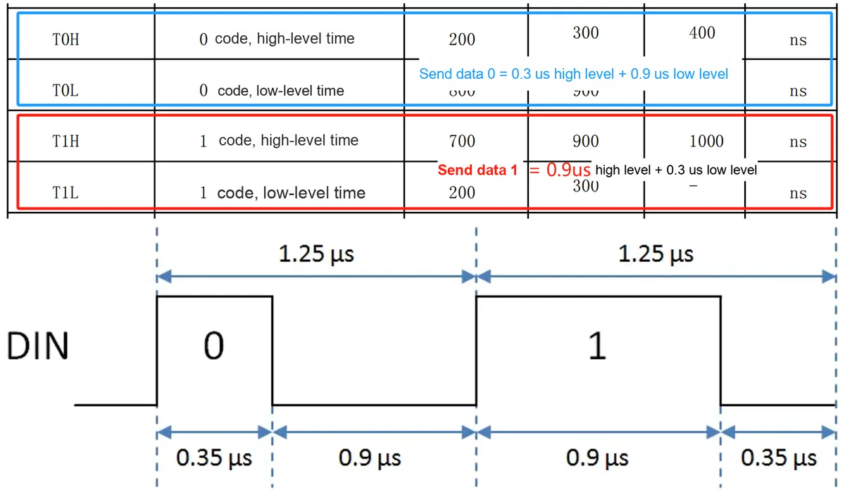
The WS2812 has a communication frequency of 800 kHz. Multiplying this by 10 gives 8 MHz (meaning one WS2812 clock cycle equals 10 PIO execution clock cycles). By controlling the high and low level output of each PIO execution clock cycle, the output binary data can be controlled:
- First, output a high level lasting for 3 PIO execution cycles on
DIN(denoted as T1 = 0.375 us here) - Adjust the high and low levels output on
DINaccording to the data bits to be transmitted (1 = high level, 0 = low level),
and maintain the level for 4 PIO execution cycles (here denoted as T2 = 0.5 us)
- Finally, pull low
the level on DINand hold it for 3PIOexecution cycles (T3 = 0.375 us)
For convenience, we refer to these three stages as T1, T2 and T3, with a ratio of 3:4:3.
    T1    T2    T3
  └─────┴─────┴─────┘ = 1.25 us
    3  :  4  :  3       T1+T2 or T2+T3 = 0.875 us
1 = high    high    low
0 = high    low    low
In the PIO program section, we first use the @rp2.asm_pio decorator to enable autopull automatic data loading, with an automatic loading threshold of 24 bits. When the data in the OSR reaches 24 bits, the OUT instruction will be automatically executed to load data from the TX FIFO and perform corresponding operations; we only need to OUT the data we want to send.
PIO The program operation process is as follows:
# Define an asm_pio function used to generate a PIO program
# Specify that the initial state of the side-set pin is low
# Specify that the shift direction of the output data is left
# Enable autopull for automatic data loading, with an autopull threshold of 24 bits
@rp2.asm_pio(sideset_init=rp2.PIO.OUT_LOW,
             out_shiftdir=rp2.PIO.SHIFT_LEFT,
             autopull=True, pull_thresh=24)
def ws2812() -> None:
    """
    Define the PIO program for the WS2812 LED driver.

    Args:
        None

    Returns:
        None

    Description:
        This PIO program drives a WS2812 LED strip and controls the output of LED color data through the state machine.
        The program outputs high and low level signals through the side-set pin to control the LEDs on and off.
    """
    # Mark the start of the program. When the program reaches wrap(), it jumps back here and continues executing
    wrap_target()
    # Define a label named bitloop, used to loop over the data of each LED
    label('bitloop')
    # Output 1 bit of data from the osr register to the x register; first execute a side-set operation to set the side-set pin low for 2 cycles
    out(x, 1).side(0)[2]
    # jmp checks whether the value of the X scratch register is 0; if it is 0, jump to the do_zero label
    # The delay of jmp is executed after the condition check, so it takes 2 + 1 cycles in total
    jmp(not_x, 'do_zero').side(1)[2]
    # If the value of X is 1, pioasm executes the third line
    # This line does not change the side-set level, so it stays high (3 + 1 cycles) and jumps back to the bitloop label
    jmp('bitloop')[3]
    # Define a label named do_zero to handle bits with value 0
    label('do_zero')
    # If the value of X is 0, nop() is executed and side-set is set low; the time is also 3 + 1 cycles
    nop().side(0)[3]
    # After the program finishes, it jumps back to wrap_target() and continues execution
    wrap()
When sending data 1, the following operations shall be performed:
out(x, 1)
 ↓
jmp(not_x, 'do_zero')
 ↓
jmp('bitloop')
When sending data 0, the following operations shall be performed:
out(x, 1)
 ↓
jmp(not_x, 'do_zero')
 ↓
nop()
 ↓
wrap()
During the aforementioned data transmission phase, a total of 7 clock cycles are consumed to complete phases T1 and T2.
Now, the PIO program returns to the start, uses the OUT instruction to fetch a piece of data, and sets the side-set pins to a low level; its execution time (2 + 1 PIO execution cycles) will become the T3 phase of the previous PIO LED. Even when the last bit of the GBR data for the final LED has been written and there is no remaining data in the OSR, the delay of the OUT instruction will still continue to complete the T3 phase of the last data.
The overall Sequence Diagram is shown as follows:
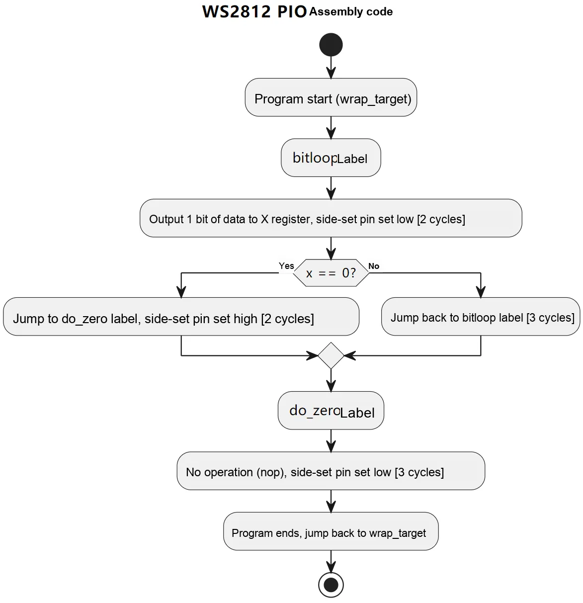
When transmitting GBR data for LED lights, we use the following statement:
# Output the color data of each LED in turn
for r, g, b in colors:
    # Shift the red, green and blue values left by 8, 16 and 24 bits respectively, then add them to form a 24-bit GRB value
    value = (g << 16) | (r << 8) | b
    # The sm.put() method actually writes 32-bit data to the FIFO
    # Shift left by 8 bits when writing to the FIFO
    sm.put(value, 8)
Here, we shift the three values of red, green, and blue left by 8 bits, 16 bits, and 24 bits respectively, then add them up to convert them into a 24-bit GRB value. It should be noted that when the WS2812 reads data, the MSB comes first and the LSB comes last. Meanwhile, the OSR shift register is 32 bits in size. To enable the WS2812 to read data starting from the MSB, we need to shift the GRB value left by 8 bits. For the missing lower 8 bits of data, the PIO state machine will suspend execution and wait for the arrival of the next 32-bit data.Here, when enabling the autopull function for automatic data loading, we set the auto-loading threshold to 24-bit data. Therefore, after the OUT module completes transmitting the 24-bit GRB data corresponding to one LED, it will automatically load the 24-bit GRB data for the next LED from the TX FIFO (note that the actual data size loaded by OUT is 32 bits, with the lower 8 bits being invalid).
In the main loop, we use the following statement to perform a left cyclic shift on the color list (each iteration shifts all elements in the list left by one position cyclically), so as to achieve the effect of the WS2812 colorful flowing LED light (visually, the corresponding color of each LED keeps shifting to the left):
colors = colors[1:] + [colors[0]]Wherein:
colors[1:]: This syntax is used to get all elements from the second element to the last one in the listcolors. In other words, this operation will return a new list that contains all elements except the first one.[colors[0]]: This syntax creates a new list that contains only the first element of thecolorslist.colors[1:] + [colors[0]]: This operation concatenates the two lists mentioned above to generate a new list, where the first element of the new list is the second element of the original list, and the last element of the new list is the first element of the original list.
This left shift operation can be used to implement the cyclic color change effect of the LED strip. Each time this line of code is executed, the elements in the color list will shift one position to the left, thereby displaying different color combinations. The overall flow of the above program is shown in the following figure:
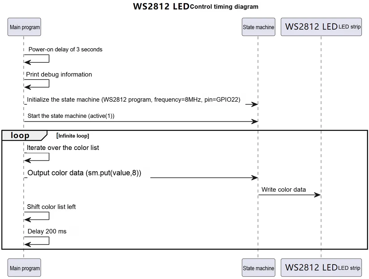
After burning the code to the Pico, you can see that the WS2812 LED strip achieves the effect of cyclic color changes of the LEDs:
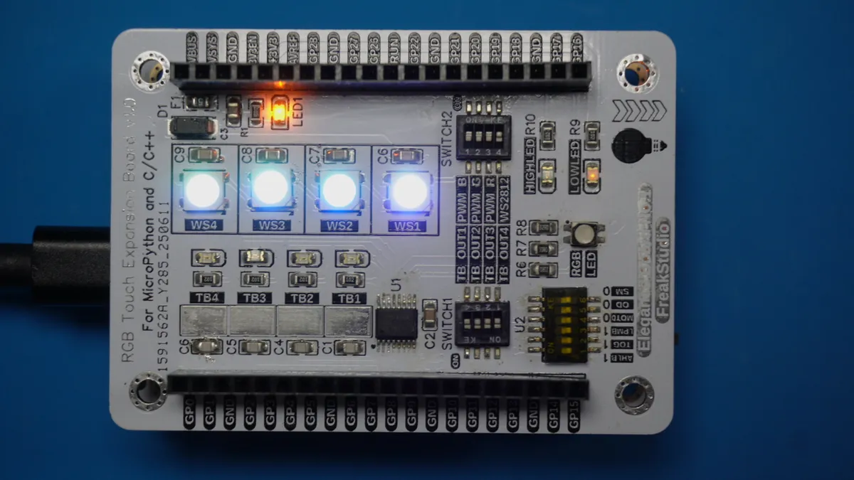
3.4.3 Application Experiment.mp4 15.5 MB
3.5 PIO Control of Stepper Motors
Here, we use PIO to implement single-phase drive control for stepper motors. Simply put, the single-phase drive control method achieves precise angle and speed control of the motor by regulating the on-off sequence and frequency of the 4 winding pairs of the stepper motor. For details, please refer to Section 4 GPIO General Purpose Input/Output for the introduction to stepper motors, which will not be repeated here.
As can be seen, when previously using GPIO to drive a stepper motor, it is usually necessary to control the pin status through loops and delays in the main program. This method will block the main program, causing the CPU to be unable to handle other tasks at the same time. In contrast, PIO is an independent hardware peripheral that can run in parallel, allowing the main program to continue executing other tasks (such as processing sensor data, communication, etc.), while PIO takes charge of precisely controlling the stepper motor.
Furthermore, the timing control of GPIO relies on software delays (e. g., time.sleep_ms ()), whose accuracy is limited by OS scheduling and CPU load; by contrast, PIO can operate at a fixed clock frequency to deliver far more precise timing control.
Here, we use the long pin headers on the Fengya No. 1 Board - Universal Compatible Expansion Board to connect the logic input interfaces on the Fengya No. 1 Board - Stepper Motor Driver Board, and the pins used are shown in the following table:
microcontroller pin | Motor drive pin | Stepper motor pins |
GPIO2 | IN1 | A |
GPIO3 | IN2 | B |
GPIO4 | IN3 | C |
GPIO5 | IN4 | D |
GND | GND | NC |
VBUS | VCC | COMMON |
Then connect the interface of the logic output section on the stepper motor driver board to the stepper motor:
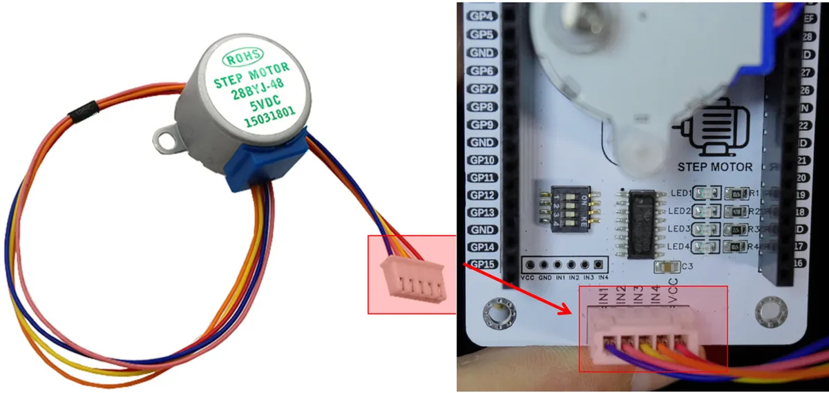
Meanwhile, toggle on the DIP switches on the Fuya No. 1 Board - Stepper Motor Driver Board:
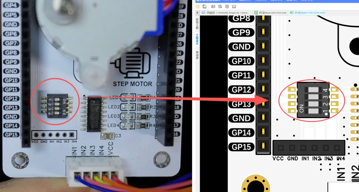
The overall connection is shown in the following figure:
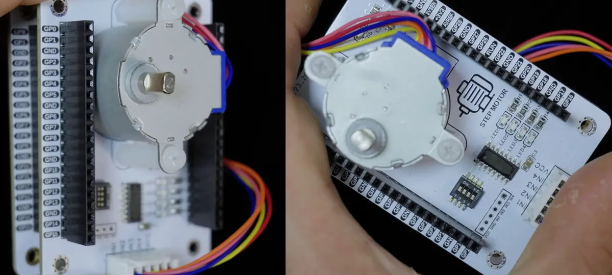
The following code can be found in the material package we provide, at the elegance-devkit v1\Demo\34 PIO_StepMotor folder.
The sample code is as follows:
# Python env   : MicroPython v1.23.0
# -*- coding: utf-8 -*-
# @Time    : 2024/7/27 1:07 PM
# @Author  : Li Qingshui
# @File    : main.py
# @Description : PIO experiment, control a stepper motor with PIO

# ======================================== Import Modules ========================================

# Import hardware-related modules
from machine import Pin
# Import PIO-related modules
import rp2
# Import time-related modules
import time

# ======================================== Global Variables ============================================

# ======================================== Functions ============================================

# The @rp2.asm_pio decorator is used to define a PIO program
# Here, it sets the initial state of 4 GPIO pins to low; these four pins are the set pins
@rp2.asm_pio(set_init=(rp2.PIO.OUT_LOW, rp2.PIO.OUT_LOW,
                       rp2.PIO.OUT_LOW, rp2.PIO.OUT_LOW))
def step_motor() -> None:
    """
    Define the PIO program for stepper motor control.

    Args:
        None

    Returns:
        None

    Description:
        This PIO program controls the rotation of the stepper motor by setting the states of 4 GPIO pins.
        Each pin is set high in turn while the other pins are low, forming a single-phase control sequence for the stepper motor.
    """
    # Marks the jump target of the program
    wrap_target()
    # Set the first pin high and the other pins low; the [7] after it means a delay of 7 clock cycles after this instruction executes
    # Since the set instruction takes 1 cycle to execute, the time interval of each stepper motor step is 1 + 7 = 8 clock cycles
    set(pins, 0b0001)   [7]
    # Set the states of the other 3 pins in turn, forming the complete single-phase control sequence of the stepper motor
    set(pins, 0b0010)   [7]
    set(pins, 0b0100)   [7]
    set(pins, 0b1000)   [7]
    # Jump the program execution back to wrap_target()
    wrap()

# ======================================== Custom Classes ============================================

# ======================================== Initialization ==========================================

# Power-on delay of 3 s
time.sleep(3)
# Print debug information
print("FreakStudio: Using PIO to control step motor")

# Initialize the state machine instance: use state machine 0 to run the step_motor() function; the PIO execution frequency equals the system clock frequency / 2000
# Set the base pin (the first of a series of pins) to GPIO 2
sm = rp2.StateMachine(0, step_motor, freq=2000, set_base=Pin(2))
sm.active(1)

# ========================================  Main Program  ===========================================

while True:
    pass
Here, in the PIO program, we use the set statement to write 4-bit binary data to control the on/off state of the 4 winding pairs of the stepper motor (setting a pin to high level will turn on one corresponding winding pair):
GPIO5 | GPIO4 | GPIO3 | GPIO2(base pin) | Stepper motor winding |
0 | 0 | 0 | 1 | A conducts |
0 | 0 | 1 | 0 | B is turned on |
0 | 1 | 0 | 0 | C conducts |
1 | 0 | 0 | 0 | D conducts |
We can also use the set statement to write decimal values 1,2, 4,8 or hexadecimal values 0x1,0x2…, and the effect will be the same.
Burn the code, and you will see the stepper motor rotate. Through the use of the PIO peripheral, we have implemented non-blocking driving for the stepper motor:
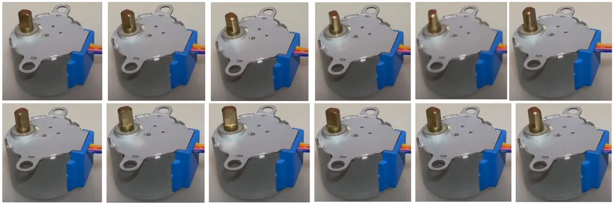
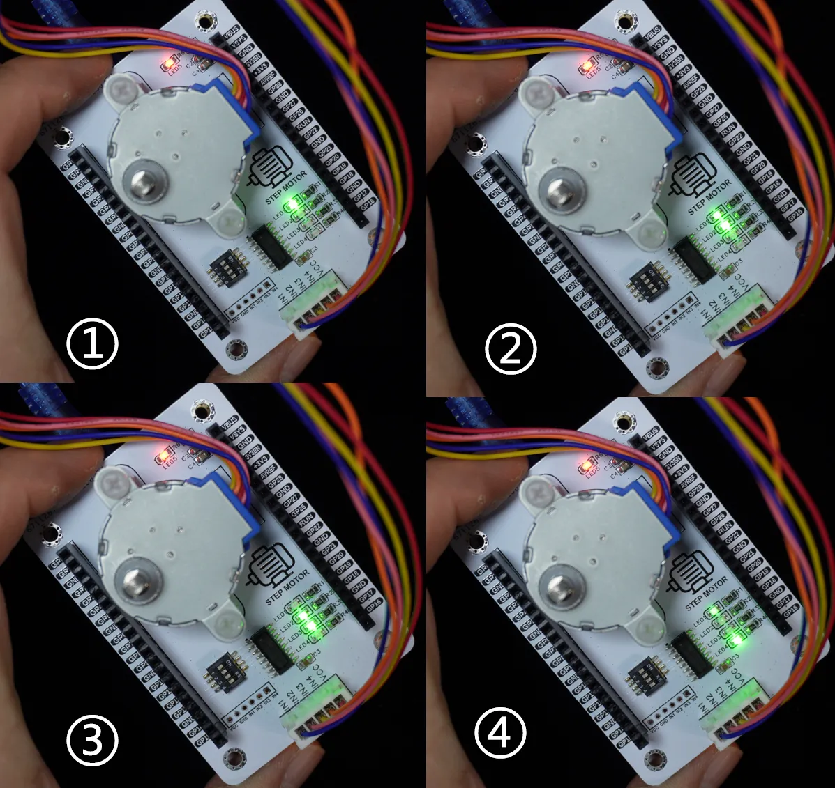
February 14.mp4 8.6 MB
3.6 Implementing UART Communication with PIO
3.6.1 Experimental Preparation
In the following experiment, we need to insert the Fengya No. 1 Board - Grove Interface Expansion Board into the Fengya No. 1 Board - Universal Compatible Expansion Board, and meanwhile use a HY2.0-4P cable to connect the Fengya No. 1 Board - Grove Interface Expansion Board 's UART1 port and the GraftSense - CH340K-based USB to TTL Module:
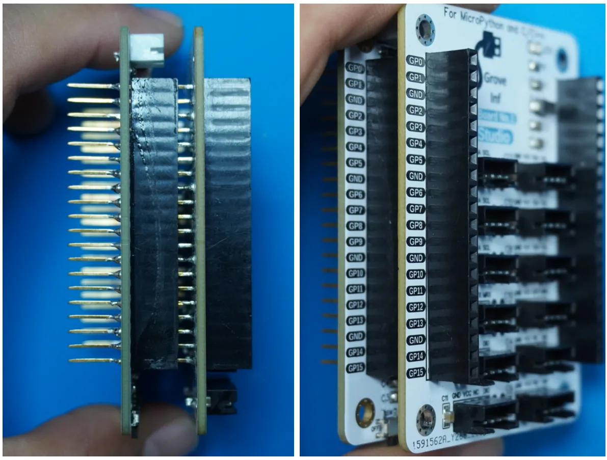
Then use a USB-A to Mini USB data cable to connect the USB port on the GraftSense - a USB-to-TTL module based on CH340K to a computer. The physical connection diagram is shown below:
In addition, we first need to connect the MiniUSB data cable to the serial port on the Fengya No. 1 Board - Universal Compatible Expansion Board. Here, GP0 and GP1 are the default pins of the hardware serial port UART0 of the Raspberry Pi Pico:
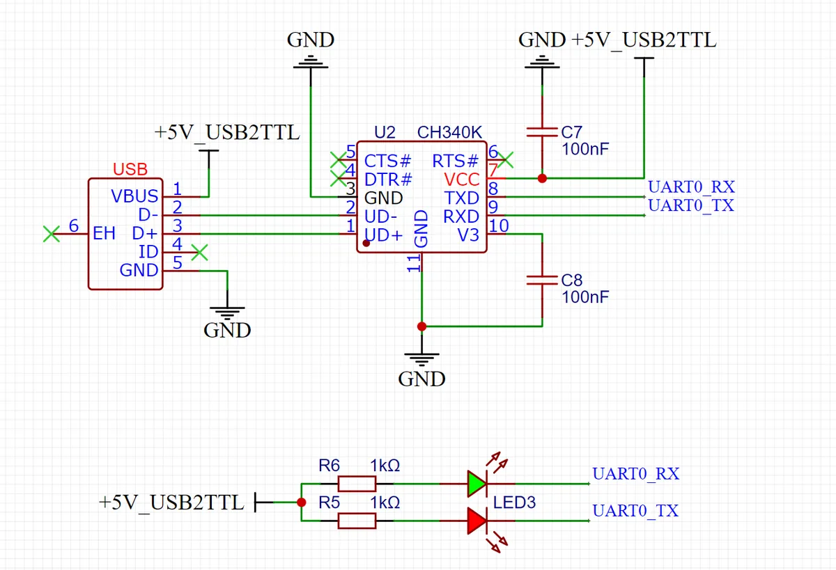
The physical image after insertion is as follows:
The pin connections are as follows:
Raspberry Pi Pico GPIO Pins | Connected electronic modules | Description of Application |
GP0 | Onboard USB-to-TTL chip | serves as the TX (transmit) pin of UART0 |
GP1 | Onboard USB-to-TTL chip | Used as the RX (receive) pin of UART0 |
GP4 | External USB to TTL module | As the side set pins and output pins (for transmission) of finite-state machine 0 |
GP5 | External USB to TTL module | Connect to an external USB-to-TTL module (presumably as the receiving pin) |
3.6.2 Implement UART Transmit Function with PIO
Here, we use PIO to implement the UART serial transmission function. First, let's recall the serial Communication Protocol: in the simplest case (without parity bit), it consists of 1 start bit, 8 data bits and 1 stop bit, and keeps a high level in the idle state:

In the PIO program, we can use the set instruction to set a high or low level to send the start bit and stop bit, and use the out instruction to send the data in the TX FIFO to the OSR shift register, thereby transmitting the data bits. In the MicroPython program, the serial port transmission function is realized by pushing the data to be transmitted into the StateMachine.put () method to push the data to be transmitted into the TX FIFO.
The following code can be found in the material package we provide at elegance-devkit v1\Demo\35 PIO_UART_TX folder.
The complete code is as follows:
# Python env   : MicroPython v1.23.0
# -*- coding: utf-8 -*-
# @Time    : 2024/7/28 1:55 PM
# @Author  : Li Qingshui
# @File    : main.py
# @Description : PIO experiment, implement UART serial communication in a PIO program

# ======================================== Import Modules ========================================

# Import time-related modules
import time
# Import RP2040-related modules
from rp2 import PIO, StateMachine, asm_pio
# Import hardware-related modules
from machine import Pin, UART

# ======================================== Global Variables ============================================

# Defines the UART baud rate as 115200
UART_BAUD = 115200
# Defines the starting pin number used by PIO as 4
PIN_BASE = 4
# Serial send count
UART_TX_COUNT = 0

# ======================================== Functions ============================================

# Timing decorator, used to measure function run time
def timed_function(f: callable, *args: tuple, **kwargs: dict) -> callable:
    """
    Timing decorator, used to measure and print function/method run time.

    Args:
        f (callable): The function/method to be passed in
        args (tuple): Any number of positional arguments passed to function/method f
        kwargs (dict): Any number of keyword arguments passed to function/method f

    Returns:
        callable: Returns the timed function
    """
    myname = str(f).split(' ')[1]

    def new_func(*args: tuple, **kwargs: dict) -> any:
        t: int = time.ticks_us()
        result = f(*args, **kwargs)
        delta: int = time.ticks_diff(time.ticks_us(), t)
        print('Function {} Time = {:6.3f}ms'.format(myname, delta / 1000))
        return result

    return new_func

# Use the @asm_pio decorator to define a PIO program
# The side-set pin is initialized high, the OUT pin is initialized high, and the output shift direction is right
@asm_pio(sideset_init=PIO.OUT_HIGH, out_init=PIO.OUT_HIGH, out_shiftdir=PIO.SHIFT_RIGHT)
def uart_tx() -> None:
    """
    PIO implementation of UART transmit logic.

    Returns:
        None
    """
    # Take one byte from the TX FIFO, wait until data is available
    pull()
    # Initialize the bit counter x to 7 and pull the pin low for 7 + 1 cycles, which is equivalent to sending a start bit
    set(x, 7)  .side(0)       [7]
    # Defines a label "bitloop" for later jumps
    label("bitloop")
    # Move a data bit from the OSR to the pins; the OUT instruction takes one cycle, with a delay of 6 cycles, 6+1 = 7 cycles in total
    out(pins, 1)              [6]
    # Decrement the x register by 1; if x is not 0, jump to the bitloop label and continue the data send loop
    # The jmp instruction takes one cycle, 7+1 = 8 cycles in total; one bitloop iteration sends one data bit
    jmp(x_dec, "bitloop")
    # No-op with a side-set operation that sets the pin high and delays 6 cycles, 6+1 = 7 cycles in total
    # The pull instruction takes one cycle, 7+1 = 8 cycles in total; sends one stop bit
    nop()      .side(1)       [6]

# pio_uart_print function, used to send a string over UART via PIO
@timed_function
def pio_uart_print(sm: StateMachine, s: str) -> None:
    """
    Send a string over UART via PIO.

    Args:
        sm (StateMachine): the PIO state machine instance to use.
        s (str): the string to send.

    Returns:
        None
    """
    # Iterate over each character in the string
    for c in s:
        # Push a word to the TX FIFO of the state machine
        sm.put(ord(c))

# Send data with the hardware UART peripheral
@timed_function
def hardware_uart_print(uart_obj: UART, s: str) -> None:
    """
    Send data with the hardware UART peripheral.

    Args:
        uart_obj (UART): the UART hardware serial peripheral instance to use.
        s (str): the string to send.

    Returns:
        None
    """
    uart_obj.write(s)
    # Block until sending is complete
    while not uart.txdone():
        pass

# ======================================== Custom Classes ============================================

# ======================================== Initialization ==========================================

# Create state machine 0, load the PIO program uart_tx, with a clock of 8 * UART_BAUD, using pin 4 as the side-set pin and output pin
sm = StateMachine(0, uart_tx, freq=8 * UART_BAUD, sideset_base=Pin(PIN_BASE), out_base=Pin(PIN_BASE))
# Start the state machine
sm.active(1)
# Create a serial port instance
uart = UART(0, UART_BAUD)
# Initialize the serial peripheral
uart.init(baudrate  = UART_BAUD,
          bits      = 8,
          parity    = None,
          stop      = 1,
          tx        = 0,
          rx        = 1,
          timeout   = 100)

# ========================================  Main Program  ===========================================

while True:
    # Delay 1 second
    time.sleep(1)
    # Send a string over UART via PIO
    pio_uart_print(sm, "UART TX DATA\r\n")
    # Send a string with the hardware UART peripheral
    hardware_uart_print(uart, "UART TX DATA\r\n")
In the PIO program section, we have completed the following work: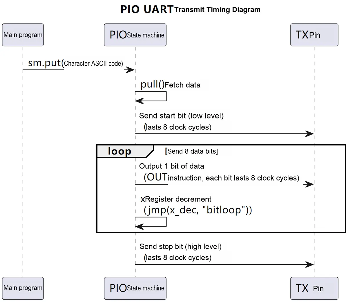
- Fetch a byte
from the TX FIFO: The program first waits untilthere is data available in the TX FIFO. This is implemented via thepullinstruction, which checks whether theFIFOis empty; if not, it fetches one byte of data fromthe FIFO. - Initialize the bit counter x: Next, the program sets the bit counter
xto 7, which means the program will transmit 8 data bits. - Start bit transmission: The program sets the pin to low level for 7 cycles, plus one additional cycle to transmit the start bit, which is implemented via the
. side (0)instruction. - Enter
bitlooploop: The program defines a label namedbitloopand starts sending data bits:- Send data bits: In the
bitlooploop, the program shifts data bits from the output shift register (OSR) to the pins. This is accomplished via theout (pins, 1)instruction, which executes for one cycle, and the program then delays for an additional 6 cycles. - Decrement bit counter x: After each data bit is transmitted, the program decrements the bit counter
xby 1 - Determine whether all data bits have been sent completely: If the bit counter
xis not 0, the program will jump back to thebitlooplabel and continue to send the next data bit; otherwise, the program will exit the loop.
- Send data bits: In the
- Send stop bit: After all data bits have been sent, the program will send a stop bit. This is achieved via the
nop ()instruction, which executes for one clock cycle. The program then delays for another 6 cycles, which combined with thepullinstruction results in a total delay of 8 cycles, completing the transmission of one stop bit.
Here, we set the clock cycle of the PIO finite-state machine to 8 * UART_BAUD to ensure correct UART timing. In the main loop, we use the pio_uart_print () function and the hardware_uart_print () function to call the PIO and hardware UART peripherals to send the same string, and compare the running speeds of the two.
Burn the code, open the remote terminal, and you can see the running speeds of two functions in the output:
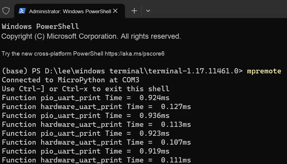
Here, we can see that the time taken to transmit 14 bytes of data via UART implemented by PIO is 0.924 ms = 924 us. At a baud rate of 115200, the time required to transmit one byte of data is 8/115200 s = 69.4 us. The expected time for us to transmit 14 bytes should be 69.4 * 14 ≈ 896 us, which is close to the time taken by the PIO-based UART to transmit 14 bytes of data (taking into account the interpreter overhead, such as type checking, function calls, etc.).
We can see that it takes 0.127 ms to send 14 bytes of data via the hardware UART peripheral. Note that this is not the actual UART transmission time, but the time taken for MicroPython function execution and calling the underlying C function:
- First, pass the pointer of the string s to the hardware UART C language driver.
- The driver copies data to the hardware FIFO buffer of the UART.
- Return immediately without waiting for all data to be sent completely.
Here, the @timed_function decorator only records the time taken for Python-C interface calls and data copying to the FIFO, rather than the physical layer transmission time.
If you want to measure the actual transmission time of the hardware UART, you can remove the commented-out code below that waits for the serial port to finish transmitting:
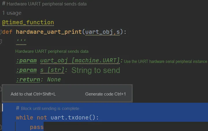
Run it again, and you can see that the serial port transmission completion time output by the terminal is about 1.2ms:
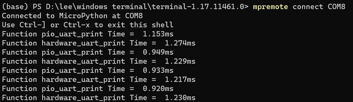
Connect GraftSense - the USB-to-TTL module based on CH340K to the computer via a data cable, then launch the XCOM serial port assistant, and we can see that the UART transmission implemented by PIO can function properly:
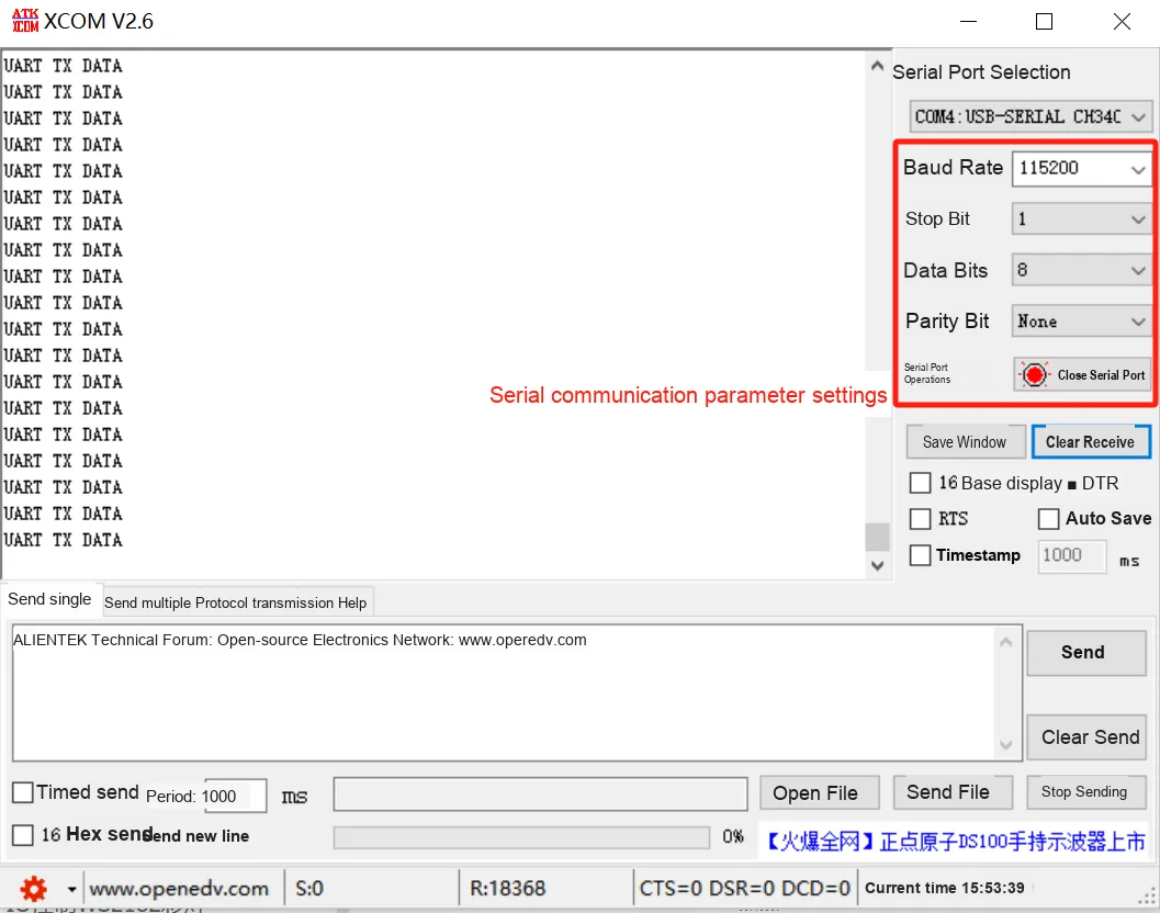
3.6.2 Application Experiment.mp4 3.6 MB
Compared with using hardware UART peripherals for serial communication, implementing serial communication via PIO offers the following advantages:
- Support for any pins:
PIOcan use any GPIO pin as a serial transmit pin, whereas a hardware UART is usually bound to specific pins; in addition, a single PIO module can implement multiple serial transmit channels simultaneously (e. g., 4 finite-state machines implement 4 UART TX channels), while the number of hardware UARTs is limited (e. g., the RP2040 only has 2 hardware UARTs). - Flexible Expansion: It can implement non-standard communication modes such as half-duplex, full-duplex, and single-wire serial port via
PIO, and also support complex frame formats (e. g., adding custom preambles, CRC checks, etc.). Meanwhile, any pin of the Raspberry Pi Pico supports PIO, which can greatly reduce the complexity of PCB layout when we make custom circuit boards.
3.6.3 Implement UART Receive Function with PIO
Here, we use PIO to implement the UART serial port receiving function. First, let's recall the serial Communication Protocol: in the simplest case (without parity bit), it consists of 1 start bit, 8 data bits and 1 stop bit, and keeps at high level in the idle state:

When communication starts, the bus transitions from idle high level to low level, and this low level serves as the start bit; subsequently, 8 data bits are transmitted in sequence (from LSB to MSB in the Sequence Diagram); after the data bits are transmitted, the bus returns to high level, which acts as the stop bit, marking the completion of one frame of data reception.
We can do the following in the PIO program:
- Detect the start bit via the
waitinstruction (wait for the pin to go low); - Use the
in_instruction to read the pin level into theISRshift register, so as to obtain the data bit; - Check whether the stop bit is at a high level (to ensure valid communication) via the
jmpinstruction; if the stop bit is normal, then push the data inpushinstruction to push the data inISRinto theRX FIFO.
In a MicroPython program, you can implement the serial receive function by reading the received data from StateMachine.get () via the RX FIFO using this method.
The following code can be found in the elegance-devkit v1\Demo\76 PIO_UART_RX folder of the resource package we provide.
The complete code is as follows:
# Python env   : MicroPython v1.23.0
# -*- coding: utf-8 -*-
# @Time    : 2025/12/23 3:56 PM
# @Author  : Li Qingshui
# @File    : main.py
# @Description : PIO experiment, implement UART serial reception

# ======================================== Import Modules ========================================

import time
from rp2 import PIO, StateMachine, asm_pio
from machine import Pin, UART

# ======================================== Global Variables ============================================

# Defines the UART baud rate as 115200
UART_BAUD = 115200
# Defines the pin number used by PIO UART reception as 5 (GP5)
PIO_RX_PIN_NUM = 5
# Defines the terminator of the received serial string
UART_TERMINATOR = '\r'
# Defines the maximum length of the received serial string (to prevent buffer overflow)
UART_MAX_STR_LEN = 128

# ======================================== Functions ============================================

# Timing decorator, used to measure function run time
def timed_function(f: callable, *args: tuple, **kwargs: dict) -> callable:
    """
    Timing decorator, used to measure and print function/method run time.

    Args:
        f (callable): The function/method to be passed in
        args (tuple): Any number of positional arguments passed to function/method f
        kwargs (dict): Any number of keyword arguments passed to function/method f

    Returns:
        callable: Returns the timed function
    """
    myname = str(f).split(' ')[1]

    def new_func(*args: tuple, **kwargs: dict) -> any:
        t: int = time.ticks_us()
        result = f(*args, **kwargs)
        delta: int = time.ticks_diff(time.ticks_us(), t)
        print('Function {} Time = {:6.3f}ms'.format(myname, delta / 1000))
        return result

    return new_func

# Use the @asm_pio decorator to define a PIO program
# The input shift direction is right
@asm_pio(in_shiftdir=PIO.SHIFT_RIGHT)
def uart_rx() -> None:
    """
    PIO implementation of UART receive logic (8 data bits, 1 start bit, 1 stop bit).

    Returns:
        None
    """
    label("start")
    # Wait for the start bit (low level)
    wait(0, pin, 0)
    # Set data counter x to 7 (8 data bits in total), and delay to the middle of the first data bit (10 cycles)
    set(x, 7)                 [10]
    # Loop to read 8 bits of data
    label("bitloop")
    in_(pins, 1)
    jmp(x_dec, "bitloop")     [6]
    # Check the stop bit (high is normal)
    jmp(pin, "good_stop")
    # Stop bit error: trigger an interrupt, wait for the pin to become idle, discard the data
    irq(block, 4)
    wait(1, pin, 0)
    jmp("start")
    # Stop bit normal: push the data to the FIFO (block means block until the FIFO has space)
    label("good_stop")
    push(block)

def uart_break_handler(sm: StateMachine) -> None:
    """
    Interrupt handler for when PIO detects a serial frame error / stop bit error.

    Args:
        sm (StateMachine): the PIO state machine instance that triggered the interrupt

    Returns:
        None
    """
    print("Recv Break/Frame Error at: {}ms".format(time.ticks_ms()))

@timed_function
def pio_uart_read_byte(sm: StateMachine) -> int:
    """
    Read one UART-received byte from the PIO state machine (with timing decorator).

    Args:
        sm (StateMachine): the PIO state machine instance to use

    Returns:
        int: the received 8-bit byte (0-255)
    """
    # Read 32-bit data from the PIO FIFO and shift right by 24 bits to extract the valid 8 bits (since right-shift storage puts them in the high 8 bits)
    received_data = sm.get()
    received_byte = received_data >> 24
    return received_byte

def pio_uart_read_string(sm: StateMachine, max_length: int = UART_MAX_STR_LEN, terminator: str = UART_TERMINATOR) -> str:
    """
    Read a UART-received string from the PIO state machine (until the terminator or maximum length).

    Args:
        sm (StateMachine): the PIO state machine instance to use
        max_length (int, optional): maximum read length, to prevent infinite blocking. Default is UART_MAX_STR_LEN
        terminator (str, optional): string terminator (such as a newline). Default is UART_TERMINATOR

    Returns:
        str: the received string
    """
    received_chars = []
    current_length = 0
    # Loop reading bytes until the maximum length is reached or the terminator is encountered
    while current_length < max_length:
        byte = pio_uart_read_byte(sm)
        char = chr(byte)
        received_chars.append(char)
        current_length += 1
        # Stop reading when the terminator is encountered
        if char == terminator:
            break
    # Join the characters into a string and return it
    return ''.join(received_chars)

# ======================================== Custom Classes ============================================

# ======================================== Initialization ==========================================

# Initialize the PIO receive pin (pull-up input, to prevent floating)
pio_rx_pin = Pin(PIO_RX_PIN_NUM, Pin.IN, Pin.PULL_UP)

# Create PIO state machine 0, load the uart_rx program, with a clock frequency of 8*UART_BAUD (a multiplier for timing matching)
# in_base: starting number of the input pins, jmp_pin: the pin used for jump decisions (same as the input pin)
sm = StateMachine(
    0,
    uart_rx,
    freq=8 * UART_BAUD,
    in_base=pio_rx_pin,
    jmp_pin=pio_rx_pin
)

# Bind the interrupt handler (triggered on a receive error)
sm.irq(uart_break_handler)
# Activate the state machine (start receiving data)
sm.active(1)

# ========================================  Main Program  ===========================================

while True:
    # Read a string (until a newline) and print it
    received_str = pio_uart_read_string(sm)
    print("Received String: {}".format(received_str))
In the PIO program section, we have completed the following work:
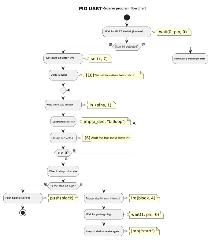
- Waiting for Start Bit: The
wait (0, pin, 0)instruction continuously monitors the pin state, and the subsequent process will not proceed until a transition of the pin from idle high level to low level (i. e., the UART start bit) is detected. - Initialization and Delay Alignment: Use
set (x, 7)to set the data counter x (corresponding to the count of 8 data bits), and at the same time delay 10 cycles via[10]to ensure that the subsequent sampling timing is aligned to the middle position of the first data bit, so as to improve sampling accuracy; - Loop to read data bits: Define a loop label via
label ("bitloop"), and usein_(pins, 1)to read the current pin level into the ISR shift register; then usejmp (x_dec, "bitloop")to decrement the counter x and jump back to the loop (until x is decremented to 0), meanwhile use[6]to delay for 6 cycles, wait for the sampling timing of the next data bit, and complete the reading of 8 data bits; - Stop Bit Check and Data Processing: After the data bits are read, check whether the pin is at a high level (i. e., the UART stop bit):
- If the stop bit is at a high level, execute the
push (block)instruction to push the 8-bit data stored in the ISR to the RX FIFO for subsequent programs to read; - If the stop bit is abnormal (not at high level), trigger a stop bit error interrupt via
irq (block, 4), then wait for the pin to return to high level usingwait (1, pin, 0), and then jump back to the start position viajmp ("start")to restart the receiving process.
- If the stop bit is at a high level, execute the
Here, we also define two functions:
def uart_break_handler(sm: StateMachine) -> None:
    """
    Interrupt handler for when PIO detects a serial frame error / stop bit error.

    Args:
        sm (StateMachine): the PIO state machine instance that triggered the interrupt

    Returns:
        None
    """
    print("Recv Break/Frame Error at: {}ms".format(time.ticks_ms()))

@timed_function
def pio_uart_read_byte(sm: StateMachine) -> int:
    """
    Read one UART-received byte from the PIO state machine (with timing decorator).

    Args:
        sm (StateMachine): the PIO state machine instance to use

    Returns:
        int: the received 8-bit byte (0-255)
    """
    # Read 32-bit data from the PIO FIFO and shift right by 24 bits to extract the valid 8 bits (since right-shift storage puts them in the high 8 bits)
    received_data = sm.get()
    received_byte = received_data >> 24
    return received_byte
Wherein:
- UART error interrupt handling function
uart_break_handler: This function is the interrupt callback function of the PIO finite-state machine, which is specifically used to handle frame errors (stop bit errors) that occur during UART reception. When the PIO assembly program detects that the stop bit is not at a high level (UART frame error / break signal), it will trigger an interrupt; - Byte Read function
pio_uart_read_byte: This function serves as the core data reading interface for PIO UART reception, which reads and parses an 8-bit UART received byte from the RX FIFO of the PIO finite-state machine.
In actual serial communication scenarios, we rarely only need to receive a single byte; more often, we receive strings (such as a line of command or a piece of text sent by the user). If we manually call pio_uart_read_byte in a loop to read bytes each time and then manually concatenate them into a string, it will be very cumbersome. For ease of use, we have also encapsulated a pio_uart_read_string function:
def pio_uart_read_string(sm: StateMachine, max_length: int = UART_MAX_STR_LEN, terminator: str = UART_TERMINATOR) -> str:
    """
    Read a UART-received string from the PIO state machine (until the terminator or maximum length).

    Args:
        sm (StateMachine): the PIO state machine instance to use
        max_length (int, optional): maximum read length, to prevent infinite blocking. Default is UART_MAX_STR_LEN
        terminator (str, optional): string terminator (such as a newline). Default is UART_TERMINATOR

    Returns:
        str: the received string
    """
    received_chars = []
    current_length = 0
    # Loop reading bytes until the maximum length is reached or the terminator is encountered
    while current_length < max_length:
        byte = pio_uart_read_byte(sm)
        char = chr(byte)
        received_chars.append(char)
        current_length += 1
        # Stop reading when the terminator is encountered
        if char == terminator:
            break
    # Join the characters into a string and return it
    return ''.join(received_chars)
Its working principle is as follows:
- continuously call the underlying function with timing function
pio_uart_read_byteto read a single byte of data from the RX FIFO of the PIO finite-state machine, convert it into the corresponding character and store it in the character list, while accumulating the character length; - During the loop, the function will check the two termination conditions in real time:
- First, check whether the length of the currently received characters reaches the preset
max_length(which is specified by the global constantUART_MAX_STR_LENby default to prevent infinite program blocking); - Second, whether the preset
terminatorhas been read (the default is the newline character\n, which is a commonly used string end marker in serial communication).
- First, check whether the length of the currently received characters reaches the preset
- Terminate the loop immediately as soon as any one of the conditions is met;
- Finally, the function concatenates the list storing characters into a complete string and returns it, thus realizing the function of directly reading a complete string from the PIO UART without requiring developers to manually handle the details of byte concatenation and termination judgment.
Here, we first connect the GraftSense - CH340K-based USB to TTL module to the computer via a data cable, then launch the xcom serial port assistant, and make sure to check the "Send New Line" option:
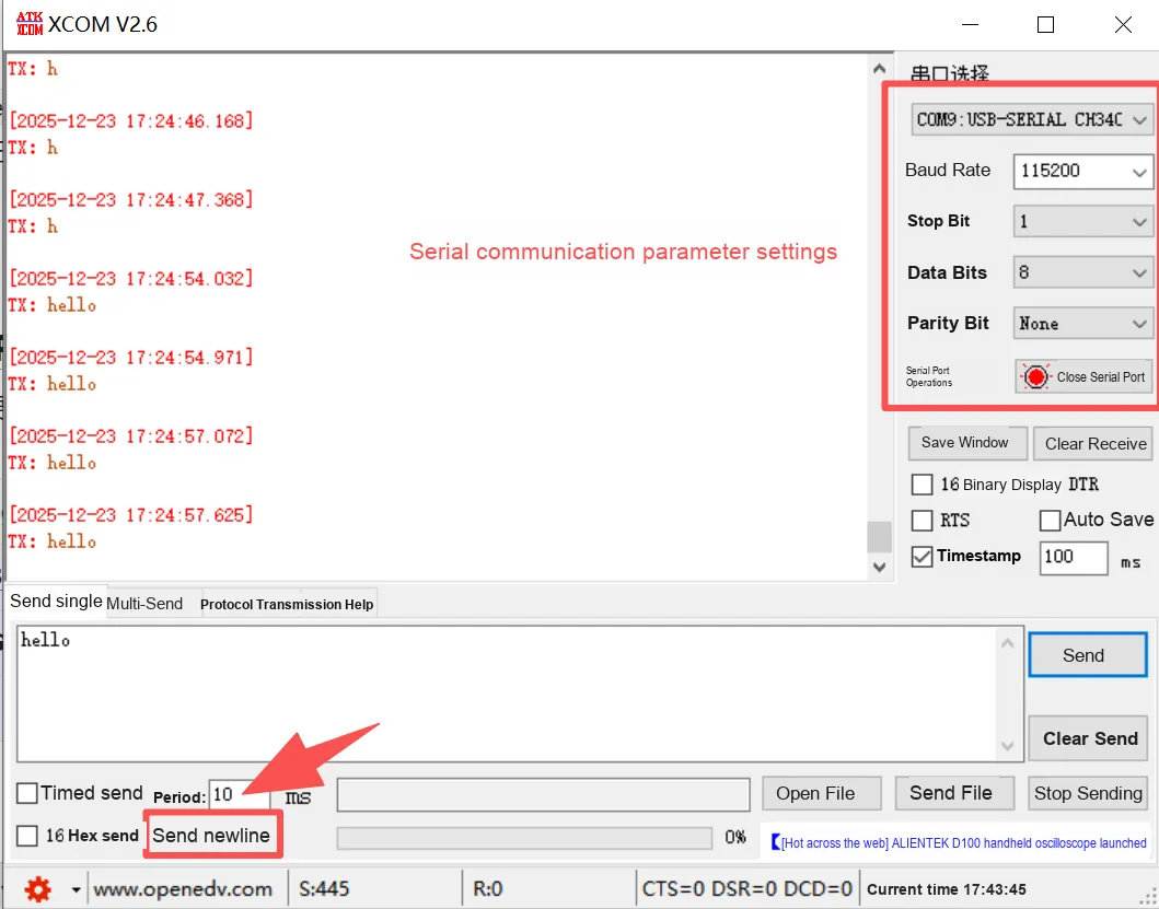
Then flash the code, open the remote terminal, and send data in the xcom serial port assistant, the terminal output is as follows:
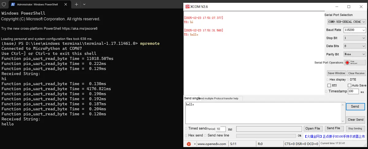
We can see that the PIO can currently be used normally to implement the serial port receiving function.
3.7 Implementing SPI Communication with PIO
Here, we need to use KingST logic analyzer to connect to the long pin header on the Fengya No. 1 Board - Universal Compatible Expansion Board:
Raspberry Pi Pico pins | Logic Analyzer Acquisition Channel | SPI Logic Adapter Board |
MOSI/MISO - GP10 | CH1 | SCLK |
CS - GP12 | CH0 | MISO |
SCLK - GP11 | CH2 | MOSI |
The pin usage of Raspberry Pi Pico is shown in the following table:
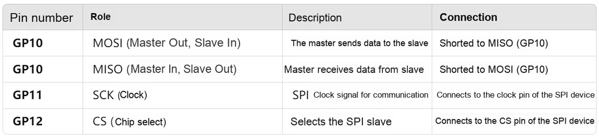
The overall physical connection effect is as follows:
3.7.1 Implementing SPI Communication Protocol with PIO
Here, we take the SPI communication with both CPOL (clock polarity) and CPHA (clock phase) set to 0 as an example to explain how to use PIO to implement the SPI Communication Protocol. First, let's recap the basic key points of SPI communication: when CPOL = 0 and CPHA = 0, the clock signal remains at a low level when no data is being transmitted, and the data is sampled on the rising edge of the clock signal (i. e., when data is sent to the receiving device, the clock signal transitions from a low level to a high level):
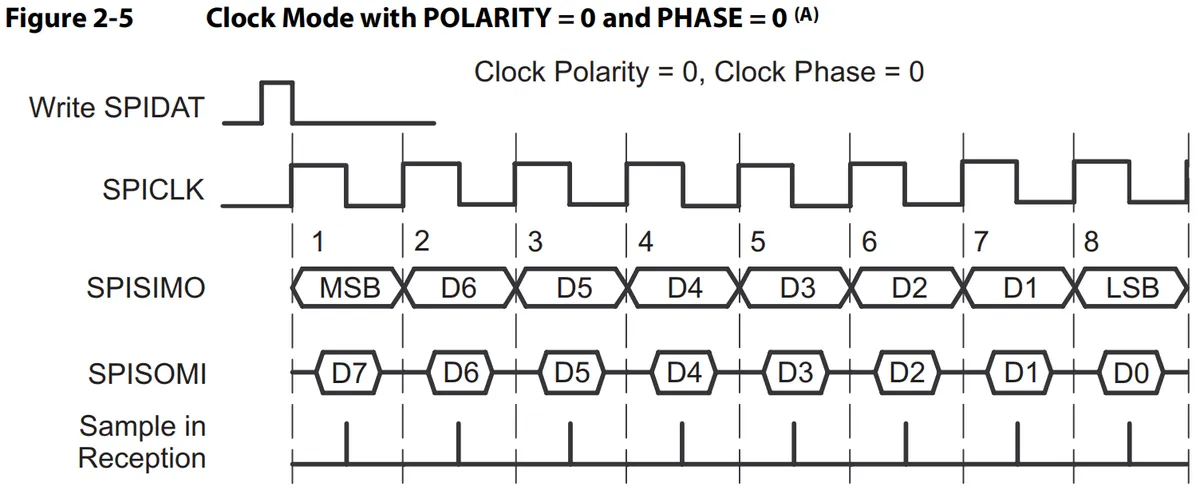
The communication process can be simplified as follows:
- When no data is being transmitted,
SCLK(clock line) remains at a low level. - At each clock cycle, data is transmitted over the
MOSI(Master Output, Slave Input) orMISO(Master Input, Slave Output) line; the data signal changes on the falling edge and is sampled on the rising edge. - Data transmission is synchronized based on the clock, and the clock changes once every time a data bit is transmitted.
Here, we modify it with reference to the official routine, and the code is as follows:
# Python env   : MicroPython v1.23.0
# -*- coding: utf-8 -*-
# @Time    : 2024/11/6 4:26 PM
# @Author  : Li Qingshui
# @File    : pio_spi.py
# @Description : PIO experiment, implement SPI protocol communication in a PIO program
# Reference code: https://github.com/raspberrypi/pico-micropython-examples/blob/master/pio/pio_spi.py

# ======================================== Import Modules ========================================

# Import hardware-related modules
from machine import Pin
# Import RP2040-related modules
from rp2 import PIO, StateMachine, asm_pio

# ======================================== Global Variables ============================================

# ======================================== Functions ============================================

# Use the @asm_pio decorator to define a PIO program
# The OSR shift register direction is left, auto-push and auto-pull are enabled, and the shift count thresholds are both 8
# The two pins used for side-set operations are initialized low and high, and the pin used for output is initialized low
@asm_pio(out_shiftdir=0, autopull=True, pull_thresh=8,
         autopush=True, push_thresh=8,
         sideset_init=(PIO.OUT_LOW, PIO.OUT_HIGH), out_init=PIO.OUT_LOW)
def spi_cpha0() -> None:
    """
    SPI protocol implemented in PIO (CPHA=0\CPOL=0)

    This PIO program implements the CPHA=0\CPOL=0 mode of the SPI protocol and supports 8-bit data transfer.
    It controls SCK and MOSI through the side-set pins while reading MISO data.

    Args:
        None

    Returns:
        None
    """
    # Set register x to 6; here the x register is used to count down the number of bits in each byte
    # Setting it to 6 means 7 clock loops are needed; the value of x decrements from 6 to 0
    set(x, 6)

    # Used to define the loop start position
    wrap_target()
    # When the OSR output shift counter reaches its threshold (i.e. 8 data bits), one byte is fetched from the TX FIFO queue into the output shift register
    # If the TX FIFO is empty, wait for data to be filled
    # Set the clock line SCK of the side-set bits (side-set) high; [1] means wait one cycle
    pull(ifempty)            .side(0x2)   [1]

    # Define the label bitloop, representing the bit loop of one byte of data (sending and receiving each bit)
    label("bitloop")
    # Take 1 bit from the output shift register OUT and output it through pins, i.e. output the data to the MOSI pin
    # Set SCK low, indicating data is output on the falling edge of the clock
    out(pins, 1)             .side(0x0)   [1]
    # Read 1 bit from the MISO pin and store it in the input ISR shift register
    # Set SCK high; data is sampled on the rising edge of the clock
    in_(pins, 1)             .side(0x1)
    # Check whether x has decreased to zero; if x has not reached zero, jump to the bitloop label to continue transferring the next bit
    # Then decrement the x register while keeping the clock high
    jmp(x_dec, "bitloop")    .side(0x1)
    # Output 1 bit of data to the MOSI pin again and set SCK low, ensuring data transmission is complete
    # A total of 8 data send/receive operations are performed, i.e. one byte of data transfer is complete
    out(pins, 1)             .side(0x0)
    # Reset the x register to 6, preparing for the next byte transfer
    set(x, 6)                .side(0x0)
    # Read 1 bit from the MISO pin and store it in the input ISR shift register
    # Set SCK high; data is sampled on the rising edge of the clock
    in_(pins, 1)             .side(0x1)

    # If OSR is not empty (its threshold has not yet been reached), jump to bitloop and continue transmitting the next byte
    jmp(not_osre, "bitloop") .side(0x1)

    # No-op that also sets SCK low, creating a delay at the end of CS, indicating that one byte of data has been transferred
    nop()                    .side(0x0)   [1]
    # Used to define the end of the loop
    wrap()

# ======================================== Custom Classes ============================================

# Custom SPI driver class implemented with the RP2040 PIO (Programmable I/O) system
class PIOSPI:
    """
    PIOSPI class, used to implement SPI communication through PIO.

    This class encapsulates SPI communication functionality based on the RP2040 PIO and supports blocking read and write operations.
    Implements the SPI protocol through a PIO state machine, suitable for SPI communication scenarios that require high efficiency and low latency.

    Attributes:
        _sm (StateMachine): PIO state machine instance, used to implement the SPI protocol.
        _cs (Pin): CS pin instance, used to control the chip select signal of the SPI device.

    Methods:
        __init__(self, sm_id, pin_mosi, pin_sck, pin_miso=None, pin_cs=None, cpha=False, cpol=False, freq=1000000):
            Initialize a PIOSPI class instance.

        write(self, wdata: list[int]) -> None:
            Write data to the SPI device in blocking mode.

        read(self, n: int) -> list[int]:
            Read data from the SPI device in blocking mode.

        write_read(self, wdata: list[int]) -> list[int]:
            Write data to and read data from the SPI device in blocking mode.
    """
    def __init__(self, sm_id: int, pin_mosi: int, pin_sck: int, pin_miso: int = None, pin_cs: int = None, cpha: bool = False, cpol: bool = False, freq: int = 1000000):
        """
        Initialize a PIOSPI class instance.

        Args:
            sm_id (int): State machine number.
            pin_mosi (int): MOSI pin number.
            pin_sck (int): SCK pin number.
            pin_miso (int): MISO pin number, optional.
            pin_cs (int): CS pin number, optional.
            cpha (bool): Clock phase, default is False.
            cpol (bool): Clock polarity, default is False.
            freq (int): Clock frequency, default is 1000000 Hz.

        Raises:
            AssertionError: If cpol or cpha is not False.
        """
        # Make sure only CPHA=0 and CPOL=0 are used (inverted clock signals or other phases are not supported)
        assert(not(cpol or cpha))

        # Check whether the pin_mosi number and pin_sck number are adjacent, and whether the pin_mosi number is less than the pin_sck number
        if not (pin_mosi == pin_sck - 1 or pin_mosi == pin_sck + 1):
            raise AssertionError('pin_mosi must be adjacent to pin_sck')

        # Create a state machine object _sm and activate it; the state machine program is spi_cpha0, with a frequency of 4*freq
        self._sm = StateMachine(sm_id, spi_cpha0, freq=4*freq, sideset_base=Pin(pin_sck), out_base=Pin(pin_mosi), in_base=Pin(pin_miso))

        # Initialize the CS pin (if provided)
        self._cs = Pin(pin_cs, Pin.OUT) if pin_cs is not None else None
        if self._cs:
            # Initial state is high (not selected)
            self._cs.value(1)

        # Activate the state machine
        self._sm.active(1)

    def write(self, wdata: list[int]) -> None:
        """
        Write data to the SPI device in blocking mode.

        Args:
            wdata (list[int]): List of data to write, each element is 8-bit data.

        Returns:
            None
        """
        # Pull the CS pin low
        if self._cs:
            self._cs.value(0)

        # Shift each byte left by 24 bits and put it into the state machine's output FIFO
        for b in wdata:
            self._sm.put(b << 24)

        # Pull the CS pin high
        if self._cs:
            self._cs.value(1)

    def read(self, n: int) -> list[int]:
        """
        Read data from the SPI device in blocking mode.

        Args:
            n (int): Number of data bytes to read.

        Returns:
            list[int]: List of data read, each element is 8-bit data.
        """
        # Pull the CS pin low
        if self._cs:
            self._cs.value(0)
        data = []

        # Clear the RX FIFO
        self._sm.restart()

        for i in range(n):
            # Take the first 16 bits of the data
            data.append(self._sm.get() & 0xff)

        # Pull the CS pin high
        if self._cs:
            self._cs.value(1)

        return data

    def write_read(self, wdata: list[int]) -> list[int]:
        """
        Write data to and read data from the SPI device in blocking mode.

        Args:
            wdata (list[int]): List of data to write, each element is 8-bit data.

        Returns:
            list[int]: List of data read, each element is 8-bit data.
        """
        # Pull the CS pin low
        if self._cs:
            self._cs.value(0)
        rdata = []

        # Clear the RX FIFO
        self._sm.restart()

        for b in wdata:
            # Shift each byte left by 24 bits and put it into the state machine's output FIFO
            self._sm.put(b << 24)
            # Take the first 16 bits of the data
            rdata.append(self._sm.get() & 0xff)

        # Pull the CS pin high
        if self._cs:
            self._cs.value(1)

        return rdata

# ======================================== Initialization ==========================================

# ========================================  Main Program  ===========================================
In this code, the decorator @asm_pio is first used to define the basic configuration of the program, including setting the OSR shift direction to left shift, enabling automatic push and automatic pull, with a shift count threshold of 8, which means each data byte contains 8 data bits, and the PIO will wait for 8 clock cycles before shifting once; it initializes the pins for SPI clock and other operations, while both the MOSI and SCK pins are initialized to a low level.
Next, in the PIO assembly program, we first use set (x, 6) to set the initial value of register x to 6, which means that 7 clock cycles are required each time to send 1 bit of data, and the x register here controls the number of cycles per operation.
Then we define the SPI protocol data transmission process. First, we use wrap_target () and wrap () to wrap the entire data transmission process, which means that after each byte is transmitted, the next byte can be transmitted continuously:
- Data Pull:
pull (ifempty)indicates pulling data from theTX FIFOqueue; if the FIFO is empty, it will wait until data is filled, and viaside (0x2)the SCK signal is set to high level, indicating the start of data transmission. - Bit loop for data transmission and reception: Data transfer is implemented using the
bitlooptag, which cyclically transmits and receives each bit:- Output data bit: Use
out (pins, 1)to output 1-bit data from the output shift register (OSR) to theMOSIpin, and set the clock lineSCKto low level viaside (0x0), indicating that data transmission is performed on the falling edge of the clock - Read data bit: Use
in_(pins, 1)to read 1 bit of data from the MISO pin into the input shift register (ISR), and setside (0x1)to pullSCKhigh, indicating that data is sampled on the rising edge of the clock - Jump judgment: passed
the jmp (x_dec, "bitloop")instruction decrements thexregister by 1 and continues the loop until all data bits have been transferred
- Output data bit: Use
- Complete one-byte transmission: When the 8 bits of one byte have been transmitted, set
xto 6 and start a new byte transmission; output the last bit of data viaout (pins, 1)and setSCKto low level to indicate that data transmission is completed - Check whether to continue:
jmp (not_osre, "bitloop")means that if the output shift register (OSR) has not reached its threshold of 8 and theFIFOqueue still contains data, the data transmission will continue in a loop - No-operation wait delay:
nop (). side (0x0)is used to wait for a certain period after the transmission is completed to create a delay for theCSsignal, which marks the end of one-byte transmission.
The overall Sequence Diagram is shown as follows:
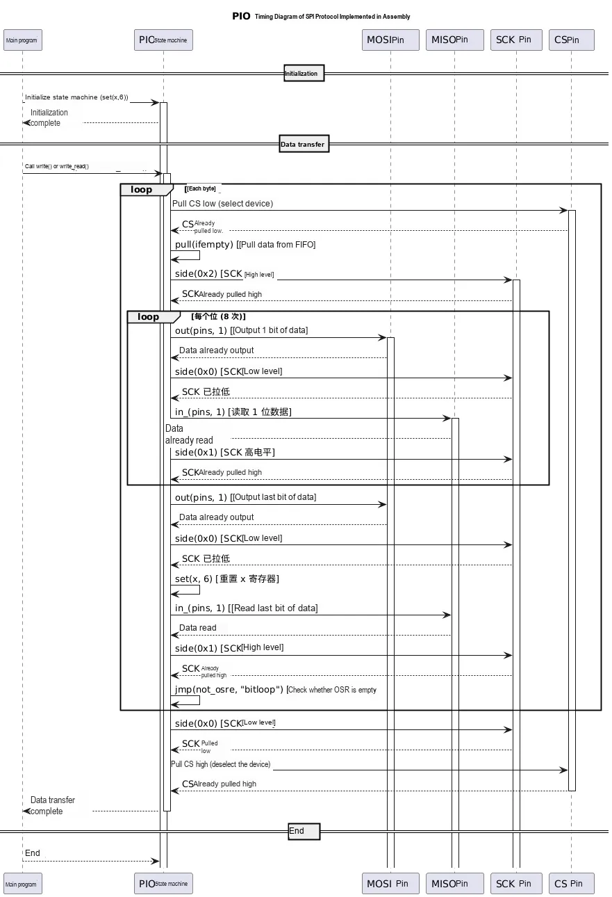
Simply put, we mainly implement SPI communication via PIO through the following steps:
- At each clock cycle, each bit of the data is shifted out from the output shift register (
OSR) to theMOSIpin, transmitted on the falling edge of the clock, while data is sampled on the rising edge of the clock. - The number of data bit transmissions per byte is controlled via
the xregister, and the program prepares the data for the next byte after each byte is transmitted. - Use
the side ()instruction to control the level change of the SPI clock (SCK) pin, ensuring that the timing of data transmission and sampling meets the requirements of CPHA= 0 and CPOL= 0.
Next, we encapsulated in the custom PIOSPI class the function of implementing SPI communication using a PIO finite-state machine, and provided the following methods: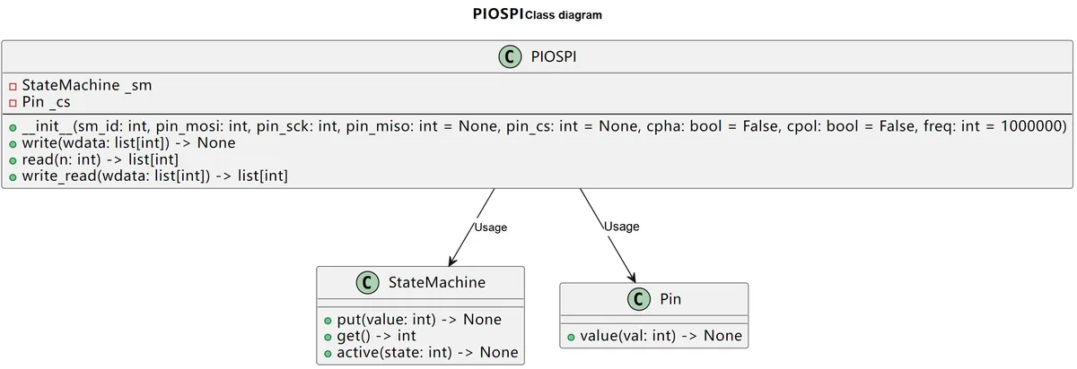
- Initialization
init ()method: Initializes the PIO finite-state machine by specifying parameters includingsm_id(finite-state machine ID),pin_mosi(data output pin),pin_miso(data input pin), andpin_sck(clock pin), sets the frequency to4*freqto adapt to the clock cycles of PIO instructions (each bit-level data operation occupies one clock cycle), and then activates the finite-state machine to prepare for data transmission. - The write
write ()method: It uses theself._sm.put ()method to shift each byte left by 24 bits (align to the most significant bit) before passing it into the TX FIFO; this is a blocking method that waits until all data has been fully transmitted.
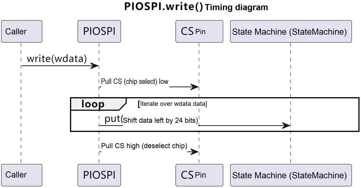
- The read
read ()method: usesself._sm.get ()to read data from the RX FIFO byte by byte, and uses& 0xffto mask the lowest 8 bits to ensure the data stays within 1 byte range; this is also a blocking method.
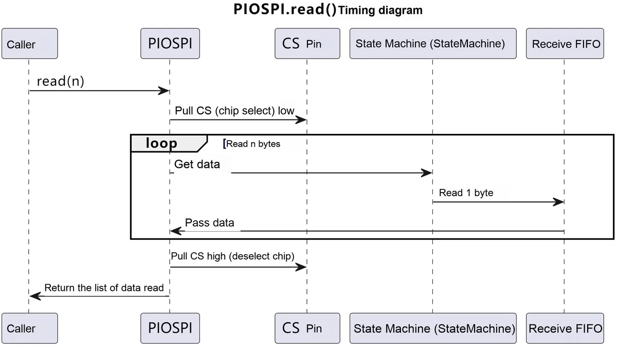
- Read-write
write_read ()method: Simultaneously transmits and receives data. It usesputto send each byte, and simultaneously callsgetto receive the corresponding response data.
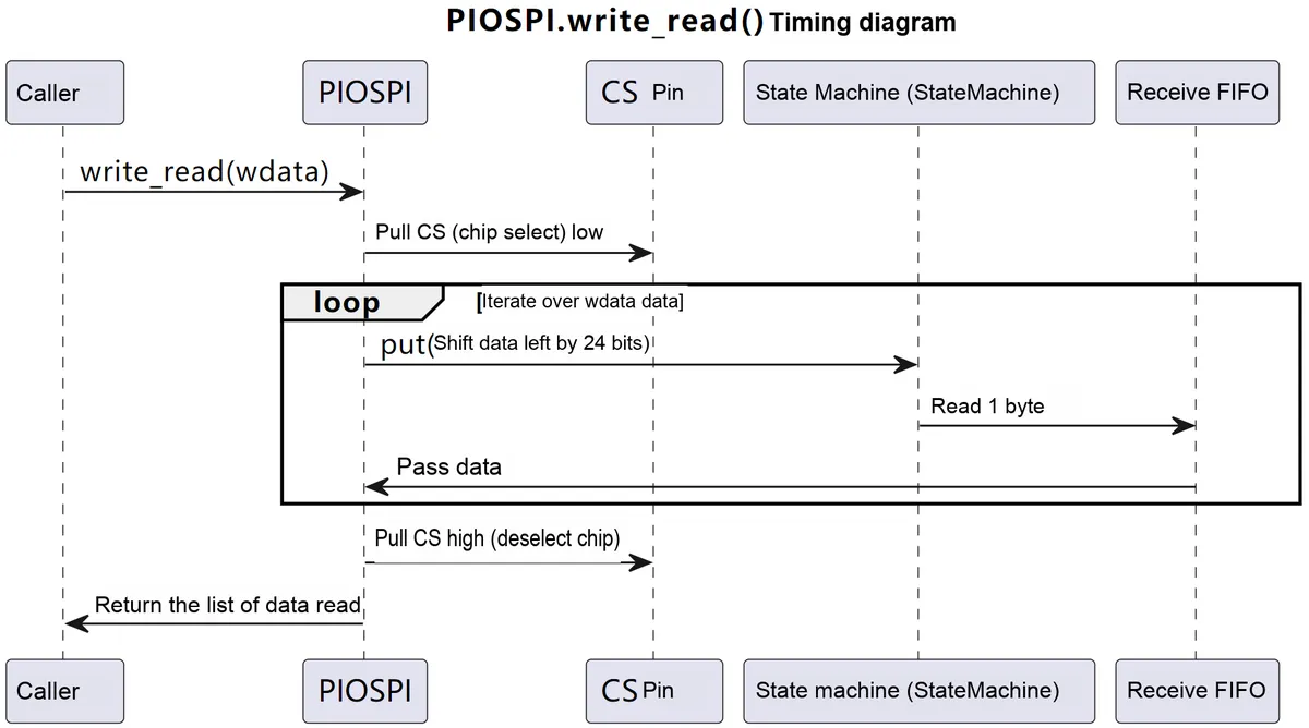
Here, it should be noted that since the PIO assembler involves settings related to side-set operations, it is required that pin_mosi and pin_sck have consecutive numbers, and the number of pin_mosi shall be smaller than that of pin_sck.
3.7.2 SPI Data Transmit-Receive Loopback Test
The following code can be found in the material package we provide elegance-devkit v1\Demo\36 PIO_SPI folder.
In the main program, we use the custom PIOSPI class to send data to external devices. The main program sends a set of byte data every second, and configures the MOSI pin to be identical to the MISO pin to perform a data transmit-receive loopback test. The sample code is shown below:
# Python env   : MicroPython v1.23.0
# -*- coding: utf-8 -*-
# @Time    : 2024/11/6 6:41 PM
# @Author  : Li Qingshui
# @File    : main.py
# @Description : Loopback test of data transmission and reception using the SPI protocol emulated with PIO

# ======================================== Import Modules ========================================

# Import time-related modules
import time
# Import the modules related to the PIO-emulated SPI protocol
from pio_spi import PIOSPI

# ======================================== Global Variables ============================================

# List of bytes to send
tx_list = [0, 1, 2, 3, 4, 5, 6, 7]

# ======================================== Functions ============================================

# ======================================== Custom Classes ============================================

# ======================================== Initialization ==========================================

# Delay to wait for the device to initialize
time.sleep(3)
# Print debug information
print('FreakStudio : Using PIO to implement the SPI protocol')

# Initialize the SPI class, set the baud rate, polarity, phase, clock pin, and data pin
# Set pin_mosi and pin_miso to GP10, pin_sck to GP11, pin_cs to GP12, CPHA to False, CPOL to False, baud rate to 1000000
# Set the MISO and MOSI pins to be the same for a send/receive loopback test
spi = PIOSPI(sm_id=0, pin_mosi=10, pin_sck=11, pin_miso=10, pin_cs = 12,cpha=False, cpol=False, freq=1000000)

# ========================================  Main Program  ===========================================

# Send and receive data using the PIO-emulated SPI protocol
while True:
    # Send and read data
    data = spi.write_read(tx_list)
    # Print debug information
    print('FreakStudio : SPI data received : {}'.format(data))
    # Wait for 1 s
    time.sleep(1)
Before flashing the code, we need to add a KingST logic analysis software, add a SPI protocol parser, and make the following settings:
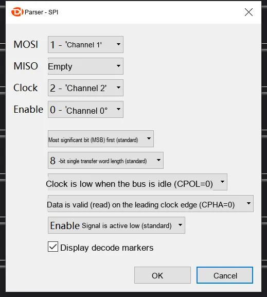
Then flash the code, open the terminal, launch the logic analyzer host software, and click to start single sampling:
The output is shown as follows:
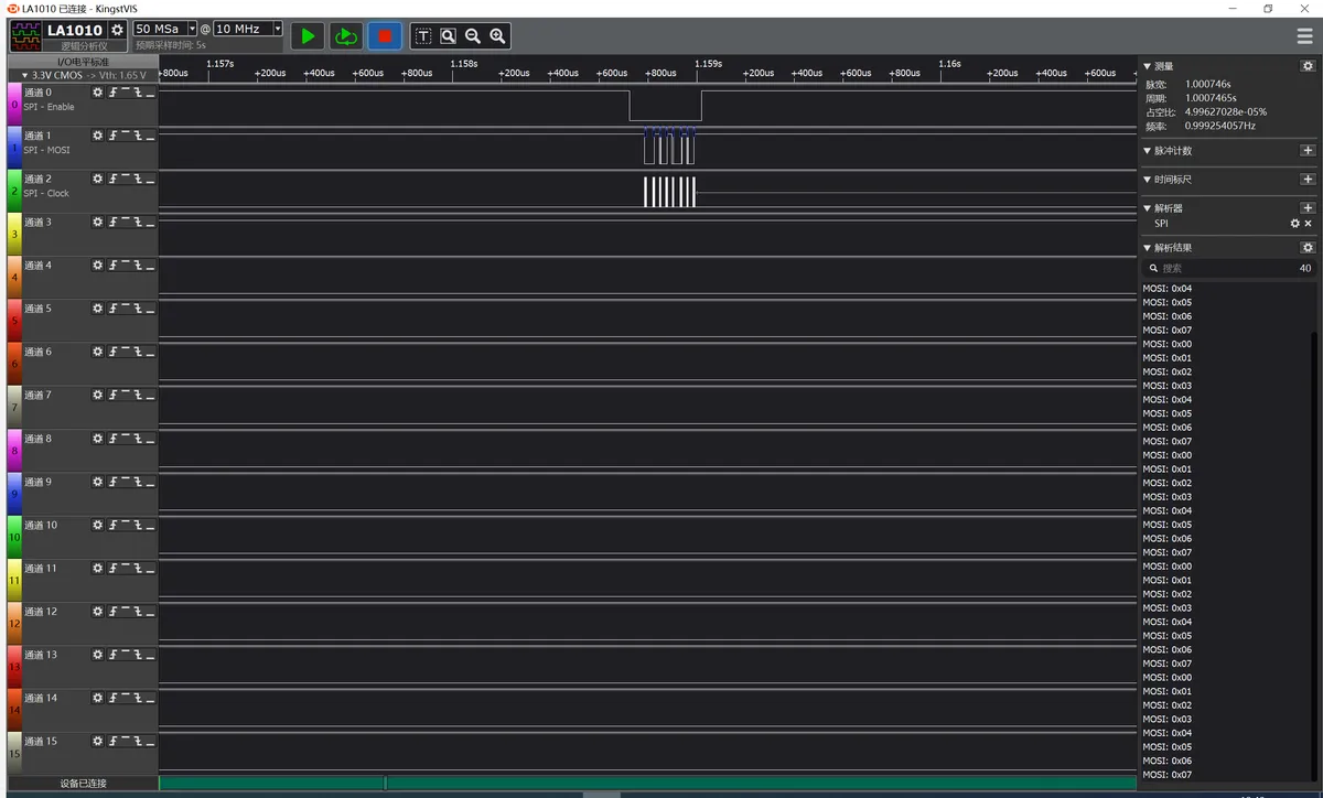
It can be seen that we have successfully used PIO to simulate the SPI protocol to send data:
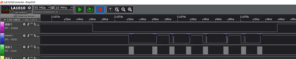
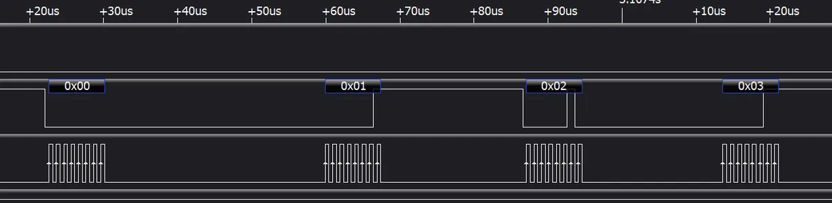
The clock frequency matches the communication frequency preset by the program:

CS The timing of the chip select pin is basically the same as the configured one: pulling it low initiates transmission, pulling it high indicates transmission completion, and the data transceive cycle is approximately 1 second.
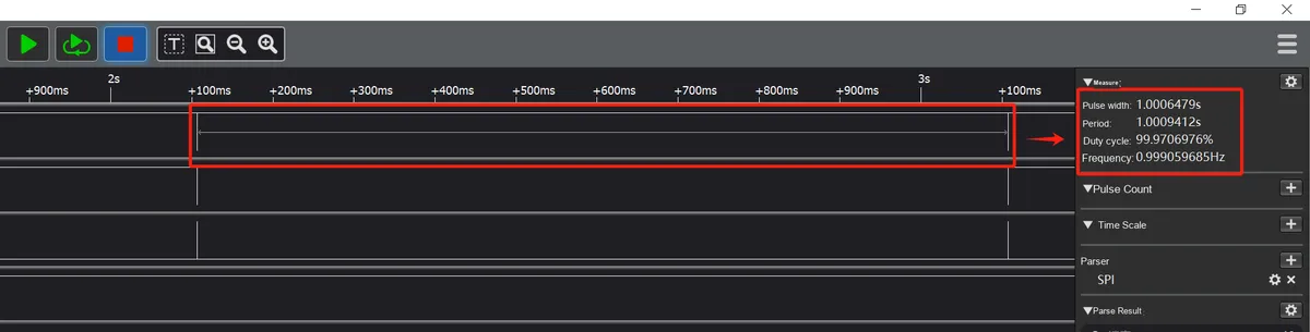

Open the terminal and connect to the Raspberry Pi Pico using the mpremote tool, and you will see that the custom PIOSPI class can complete data reception:
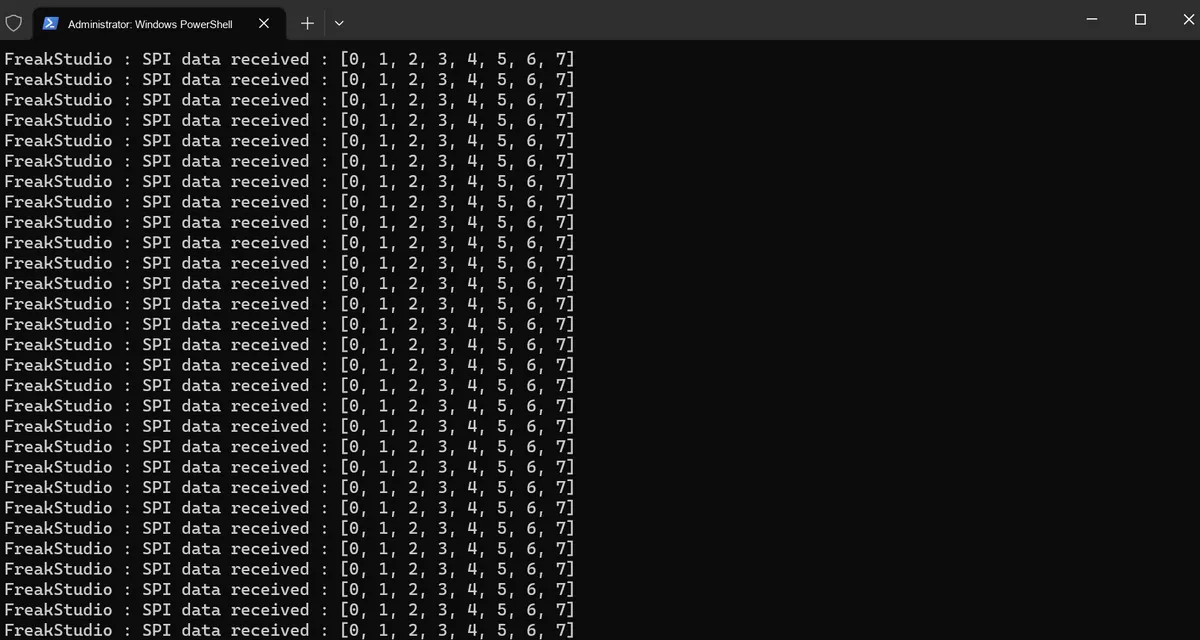
References
- Playing with the Pico Part 4 - Getting Acquainted with PIO
https://gregchadwick.co.uk/blog/playing-with-the-pico-pt4/
- Introduction to the PIO (Programmable Input Output) of the RP2040
https://tutoduino.fr/en/pio-rp2040-en/
- Raspberry Pi Pico and RP2040 - C/C++ Part 3: How to Use PIO
https://www.digikey.com/en/maker/projects/raspberry-pi-pico-and-rp2040-cc-part-3-how-to-use-pio
- A helper for PIO function help
https://www.micropython.org.cn/forum/viewtopic.php?f=30&t=1902
- RP2040 PIO, state machine and pioasm
https://alankrantas.medium.com/
- Programmable IO (PIO) of Raspberry Pi Pico
https://pico.nxez.com/2023/11/06/programmable-io-on-raspberry-pi-pico.html
- Chinese Version of RP2040 PIO Manual
https://gitee.com/hemn1990/rp2040-pio-zhcn#/hemn1990/rp2040-pio-zhcn
- RP2040 (Raspberry Pi Pico) PIO – Peripheral Overview
https://www.taterli.com/7568
- Why use programmable I/O?
https://cnx-software.cn/2021/06/06/raspberry-pi-rp2040-programmable-ios/
- Notes on Waveshare Raspberry Pi PICO – 8: PIO (Programmable Input/Output)
https://blog.csdn.net/weixin_51684355/article/details/127033371
- Programmable I/O with Raspberry Pi Pico
https://www.seeedstudio.com/blog/2021/01/25/programmable-io-with-raspberry-pi-pico/
- Plain-Language Breakdown of Raspberry Pi Pico's PIO (Programmed I/O) — Writing pioasm with MicroPython: Part I
https://alankrantas.medium.com/%E7%99%BD%E8%A9%B1%E8%A7%A3%E5%AF%86-raspberry-pi-pico-%E7%9A%84-pio-programmed-i-o-%E4%BD%BF%E7%94%A8-micropython-%E6%92%B0%E5%AF%AB-pioasm-part-i-e801a161cf98
- Programmable I/O with Raspberry Pi Pico
https://www.seeedstudio.com/blog/2021/01/25/programmable-io-with-raspberry-pi-pico/
- Playing with the Pico Part 4 - Getting Acquainted with PIO
https://gregchadwick.co.uk/blog/playing-with-the-pico-pt4/
- Chinese Version of RP2040 PIO Manual
https://gitee.com/hemn1990/rp2040-pio-zhcn/tree/master
- 【Diao Ye Learns Programming】MicroPython Manual: Specific Library neopixel — Control of WS2812 / NeoPixel LEDs
https://blog.csdn.net/weixin_41659040/article/details/132837911
- Programmable IO (PIO) of Raspberry Pi Pico
https://pico.nxez.com/2023/11/06/programmable-io-on-raspberry-pi-pico.html
examples/rp2/pio_uart_rx.py
https://github.com/micropython/micropython/blob/master/examples/rp2/pio_uart_rx.py
Version Record
Version Number | Modifier | Time | Content |
v1.0.0 | Li Zisheng | 2025/09/18 | Initialize the document, based on MicroPython version V1.23.0. The UART receive function implemented via PIO and the timer function implemented via PIO have not been realized yet. Meanwhile, the I2C protocol can also be implemented with PIO. |
v1.0.1 | Li Zisheng | 2025/12/05 | Initialize the document, based on MicroPython version V1.23.0. The UART receive function implemented via PIO and the timer function implemented via PIO have not been realized yet. Meanwhile, the I2C protocol can also be implemented with PIO. Some images have been added. |
v1.0.2 | Li Zisheng | 2025/12/22 | Optimized the content related to principle explanation (based on MicroPython V1.23.0) The UART receive function implemented via PIO and the timer function implemented via PIO have not been realized yet. Meanwhile, the I2C protocol can also be implemented with PIO. |
v1.1.0 | Li Zisheng | 2025/12/23 | Added code for PIO simulated serial port reception (based on MicroPython v1.23.0), and removed Sample code for implementing a timer with PIO. |
v1.2.0 | Li Zisheng | 2026/02/14 | Improve the stepping motor section. |