
Contents
1. Introduction
We have already learned about the basic timing of the IIC Communication Protocol, and now we can put it into practice to learn how to write code to implement the corresponding functions. Similar to serial communication, IIC communication can also be divided into software IIC and hardware IIC. In this section, we will first use software to simulate IIC communication, and manually control the level state changes of GPIO pins during the simulated communication process, so as to intuitively understand the generation process of each IIC signal.
2. Implement IIC timing
To recap, the IIC protocol mainly consists of start condition, stop condition, and data bit transmission these three parts.

During data transmission, the level changes of SCL (Serial Clock Line) and SDA (Serial Data Line) need to meet specific timing requirements, and the specific parameters can be referred to the following table:
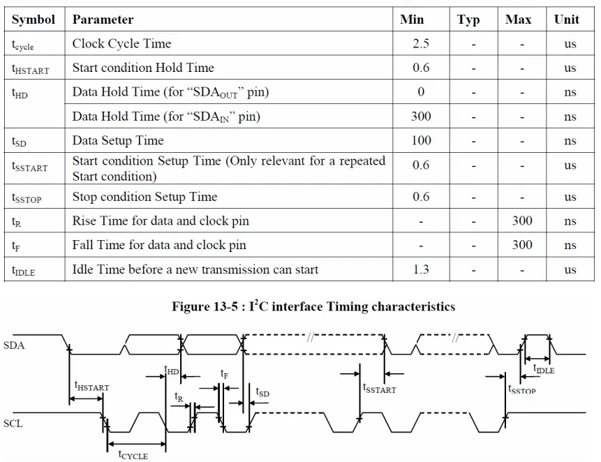
2.1 Start Signal
The timing of the start signal is: when SCL is at high level, SDA is pulled down from high level to generate the start signal. A code example is given below:
void IIC_Start(void) {
  pinMode(SDA_PIN, OUTPUT);        // Set the SDA pin as output
  digitalWrite(SDA_PIN, HIGH);     // Set SDA high
  digitalWrite(SCL_PIN, HIGH);     // Set SCL high
  delayMicroseconds(4);            // Delay 4 microseconds

  digitalWrite(SDA_PIN, LOW);      // Set SDA low to generate the start signal
  delayMicroseconds(4);            // Delay 4 microseconds

  digitalWrite(SCL_PIN, LOW);      // Set SCL low to complete the start signal
}
2.2 Stop Signal
The timing of the stop signal is: when SCL is at high level, SDA is pulled up from low level to generate the stop signal. A code example is provided below:
void IIC_Stop(void) {
  pinMode(SDA_PIN, OUTPUT);      // Set the SDA pin as output
  digitalWrite(SCL_PIN, LOW);    // Set SCL to low level
  digitalWrite(SDA_PIN, LOW);    // Set SDA low to prepare the stop signal
  delayMicroseconds(4);          // Delay 4 microseconds

  digitalWrite(SCL_PIN, HIGH);   // Set SCL high
  digitalWrite(SDA_PIN, HIGH);   // Set SDA high to send the stop signal
  delayMicroseconds(4);          // Delay 4 microseconds
}
2.3 Data Transmission
In the software I²C implementation, we simulate data transmission by controlling the level changes of the SDA and SCL pins. For each byte transmitted, the master device sends data bit by bit and waits for the slave device to return an ACK signal.
Here is a code example for data transmission:
// Write data to the I2C bus
uint8_t I2C_Write(uint8_t data) {
  // Send the 8 bits of data one by one
  for (int i = 7; i >= 0; i--) {
    // Set the SDA level
    digitalWrite(SDA_PIN, (data >> i) & 0x01);
    // Generate a clock pulse
    digitalWrite(SCL_PIN, HIGH);
    delayMicroseconds(5);  // Hold the high level for a period of time
    digitalWrite(SCL_PIN, LOW);
    delayMicroseconds(5);  // Hold the low level for a period of time
  }

  // After sending the byte, wait for ACK
  pinMode(SDA_PIN, INPUT);  // Set SDA as input (allows the slave to pull it low)
  digitalWrite(SCL_PIN, HIGH);  // Generate a clock pulse
  delayMicroseconds(5);
  uint8_t ack = digitalRead(SDA_PIN);  // Read ACK
  digitalWrite(SCL_PIN, LOW);  // Clock pulse ends
  pinMode(SDA_PIN, OUTPUT);  // Restore SDA to output mode

  return ack;  // Return the ACK bit (0 means acknowledged, 1 means not acknowledged)
}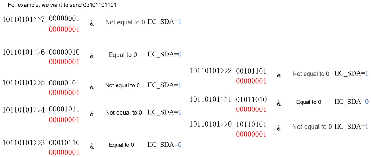
For example, if we want to send 0b10110101, the steps are as follows:
After transmitting the data, the receiver sends an acknowledge bit: when the acknowledge bit is at a low level, it is defined as a valid acknowledge bit (ACK, referred to as acknowledge bit for short), indicating that the receiver has successfully received the byte; when the acknowledge bit is at a high level, it is defined as a non-acknowledge bit (NACK), generally indicating that the receiver has failed to receive the byte correctly.
3. Example: Simple Communication Between ESP32 and OLED Display
Finally, we control the ESP32 to send the address to the OLED display and receive the acknowledgment signal. Through this simple example, you can better understand how to conduct inter-device communication via the I²C protocol.
📌 Objective
- Send an address to the OLED display to check if it responds.
- Learn the implementation of data transmission and acknowledge signals via simulated software I²C.
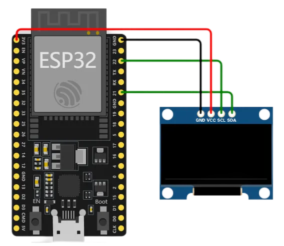
The next operation we are going to implement is to make the ESP32 (master) write the slave address to the OLED module (slave) via the IIC bus, observe that the response is ACK, and determine whether the writing is successful.
The judgment result is also very intuitive: if ACK returns 0, it indicates that the write operation is successful, meaning the slave device indeed exists; if it returns 1, it indicates that the write operation fails, which also means the slave device does not exist or is operating abnormally.
// Define the SDA and SCL pins
#define SDA_PIN 21  // Modify according to the actual hardware
#define SCL_PIN 22  // Modify according to the actual hardware

void I2C_Start()
{
  // Pull SDA and SCL low to generate the start condition
  digitalWrite(SDA_PIN, LOW);  // Pull SDA low
  delayMicroseconds(5);
  digitalWrite(SCL_PIN, LOW);  // Pull SCL low
  delayMicroseconds(5);
}

// Write data to the I2C bus
uint8_t I2C_Write(uint8_t data) {
  // Send the 8 bits of data one by one
  for (int i = 7; i >= 0; i--) {
    // Set the SDA level
    digitalWrite(SDA_PIN, (data >> i) & 0x01);
    // Generate a clock pulse
    digitalWrite(SCL_PIN, HIGH);
    delayMicroseconds(5);  // Hold the high level for a period of time
    digitalWrite(SCL_PIN, LOW);
    delayMicroseconds(5);  // Hold the low level for a period of time
  }

  // After sending the byte, wait for ACK
  pinMode(SDA_PIN, INPUT);  // Set SDA as input (allows the slave to pull it low)
  digitalWrite(SCL_PIN, HIGH);  // Generate a clock pulse
  delayMicroseconds(5);
  uint8_t ack = digitalRead(SDA_PIN);  // Read ACK
  digitalWrite(SCL_PIN, LOW);  // Clock pulse ends
  pinMode(SDA_PIN, OUTPUT);  // Restore SDA to output mode

  return ack;  // Return the ACK bit (0 means acknowledged, 1 means not acknowledged)
}

void I2C_Stop()
{
  digitalWrite(SDA_PIN, LOW);  // Pull SDA low
  delayMicroseconds(5);
  digitalWrite(SCL_PIN, HIGH);  // Pull SCL high
  delayMicroseconds(5);
  digitalWrite(SDA_PIN, HIGH);  // Pull SDA high
  delayMicroseconds(5);
}

uint8_t I2C_Address(uint8_t addr)
{
  uint8_t ack;
  I2C_Start();  // Send the start condition
  ack = I2C_Write(addr << 1);  // Write the device address; shifted left by one bit because the 8th bit of an I2C address is the read/write control bit
  I2C_Stop();  // Send the stop condition
  return ack;  // Return the ACK bit; 0 means the device responded, 1 means no response
}

void setup()
{
  Serial.begin(115200);
  pinMode(SDA_PIN, OUTPUT);
  pinMode(SCL_PIN, OUTPUT);

  uint8_t ack = I2C_Address(0x3C);  // The OLED address is 0x3C
  Serial.println(ack);

}

void loop()
{
  // Other communication logic or device interaction can be added here
}
📌 Sample Analysis
1. Initialize IIC communication
pinMode (SDA_PIN, OUTPUT) and pinMode (SCL_PIN, OUTPUT) set the SDA and SCL pins to output mode, which enables communication control over the I²C bus via these pins.
2. Send the device address and wait for the response
In the I2C_Address function, we first call I2C_Start () to send a start signal and initiate I²C communication.
Then call I2C_Write () function to send the device address (here it is 0x3C, assuming it is the I²C address of the OLED display). The device address will be shifted left by one bit to add a read-write control bit at the end of the address.
After sending the address, the main controller checks the acknowledge bit to determine whether the OLED display has successfully received the address:
If the device returns an ACK (acknowledgement), it indicates that the OLED display has successfully received the address; if a NACK (non-acknowledgement) is returned, it means that the OLED display is not responding, which may be due to an incorrect address or the device not being connected.
4. Summary of This Chapter
In this chapter, building on our prior understanding of the principles of IIC communication timing, we further implement the complete IIC communication process hands-on through software simulation. Unlike directly calling the hardware IIC peripheral, software IIC manually controls the high and low levels of GPIO pins, translating abstract protocol rules into an observable and understandable process of level changes, which helps us truly "see through" how IIC works.
By implementing the bit-by-bit transmission of the start signal, stop signal and data bits, we have revisited and verified the core timing rules of IIC: the generation conditions of the start and stop signals, the principle that data changes when SCL is at low level and is sampled when SCL is at high level, as well as the communication structure of "8-bit data + 1-bit acknowledge". Meanwhile, through the judgment of ACK and NACK, we also intuitively understood how the master confirms whether the slave device exists and whether the data is correctly received.
Finally, taking the address communication between ESP32 and OLED display as an example, we combine the aforementioned timing functions into a complete communication process, realizing the entire process from initiating communication to judging the slave response. This example not only verifies the feasibility of software IIC, but also lays a solid foundation for the subsequent use of hardware IIC or driving specific peripherals.
In the next phase of learning, we will build on these understandings of timing and logic to gradually transition to the more efficient and commonly used hardware IIC interface, and complete more complex device data read and write operations.
5. Simulation Experiment Link
Simulation Experiment Link: https://wokwi.com/projects/419482527334079489