
I2C (Inter-Integrated Circuit, communication between integrated circuits) is a common serial Communication Protocol, which is widely used for data transmission between microcontrollers and peripherals. Similar to UART, I2C can also be analyzed from the physical layer, protocol layer and application layer.
In this section, we mainly focus on the physical layer and protocol layer, which determine how I2C devices are connected, how data is transmitted, and how communication reliability is guaranteed. As for the application layer, it involves how specific devices exchange data via I2C, such as EEPROM read/write, sensor Data Acquisition, etc. This part will be explained in subsequent chapters combined with practical cases.
1. Basic Concepts
Before learning about IIC, we first need to understand the following basic concepts:
- Master: Usually a microcontroller, responsible for initiating communication, generating the clock signal (SCL), and controlling the start and end of data transmission.
- Slave: Responds to requests from the master, and receives and executes commands issued by the master. Each slave has a unique address, which the master uses to select the target device. Typical slave devices include sensors, memory chips, etc.
Certainly, the master can send commands to the slave, and the slave can also return data to the master; the roles of the data sender and receiver are both dynamically changing.
- Transmitter: A device responsible for transmitting data during communication, which can be either a master device or a slave device depending on the direction of the current data flow.
- Receiver: A device responsible for receiving data, which can be either a master device or a slave device, depending on the direction of the current data stream.
ESP32 I2C Peripheral
ESP32 has two built-in I2C hardware controllers (I2C0 and I2C1), which share identical functions and can be deployed for separate tasks simultaneously. For instance, one I2C interface can be used to connect sensors, while the other can be applied to storage devices or display modules, greatly enhancing the flexibility of the system.
2. IIC Physical Layer
2.1 IIC Interface
IIC (Inter-Integrated Circuit, inter-integrated circuit communication) has the following notable features: it is serial, synchronous, half-duplex, and only requires two wires to complete data transmission, which makes I2C a highly efficient and easy-to-implement Communication Protocol, especially suitable for low-speed devices or scenarios where pin resources are limited.
These two wires are as follows:
SCL (Serial Clock Line)
- Function: SCL is used to carry the clock signal transmitted over the I2C bus. It is controlled by the master device to generate clock pulses, and all devices (both master and slave) synchronize their data transmission and reception based on this clock signal.
- Features: During data transmission, the SCL (Serial Clock Line) periodically toggles, representing each cycle of the clock and ensuring that data is transmitted in sequence.
SDA (Serial Data Line)
- Function: SDA is used for data transmission. In I2C, data is transmitted in bytes (8 bits), and the level changes on the SDA line represent specific data bits.
- Features: The SDA line transmits data under the control of the clock signal.
2.2 IIC Communication Wiring Method
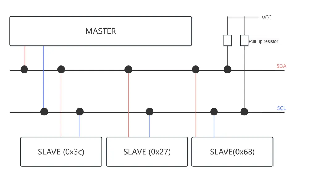
master-slave architecture
I2C adopts a master-slave architecture, and supports single-master multi-slave connection, which means:
- One master device can be connected to multiple slave devices.
- All I2C devices can share the same pair of SCL and SDA lines
The devices on the IIC bus form a "wired-AND" logic, and any device can control the level signal.
The IIC bus adopts a logic called "Wired-AND", a design that allows multiple devices to share the same pair of SCL and SDA lines, thus realizing a master-slave communication mode with one master and multiple slaves. The core concept of this approach is as follows:
- The bus remains at a high level only when all devices have released the signal line (i. e., not pulling it low).
- As long as one device pulls the signal line low, the bus level will become low, regardless of the status of other devices.
This design addresses the collision issues that may arise when multiple devices share a signal line. Why is the "wired-AND" logic adopted?
First, it prevents signal conflicts. If one device pulls a signal low while another tries to pull it high, a short circuit will occur. Under the wired-AND logic, devices only need to release the signal line instead of actively pulling it high, thus ensuring coordination on the bus.
Furthermore, it allows multiple devices to share the same pair of SCL and SDA lines without requiring additional signal lines.
Finally, it enables the device to determine the bus status. If a device intends to communicate, it can check whether the SDA line is pulled low to judge if the bus is idle, which can prevent conflicts caused by multiple devices transmitting data simultaneously.
External pull-up resistors must be connected to the IIC bus.
The signal lines of the IIC bus adopt the open-drain output (Open-Drain) mode. Its characteristic is that the device can only pull the signal low, and cannot actively pull the signal line high. This means that if there is no other method, the signal line will always remain at a low level.
To ensure that the signal line can return to a high level when it is not being pulled low, we need to use a pull-up resistor. The function of a pull-up resistor is to "pull" the signal line back to a high level. When a device is not pulling the signal low, the resistor will pull the signal line back to a high level. Typically, we use a 4.7kΩ or 10kΩ resistor to achieve this.
Each I2C device has a unique address
On the I2C bus, there may be multiple slave devices (such as multiple sensors). So how does the master know exactly which slave it is communicating with? And how does a slave tell whether the master is addressing it?
Actually, every I2C device has a unique "address", just like everyone has a unique name.
- Representation of Device Addresses: When transmitted over the I2C bus, device addresses typically consist of 7 bits or 10 bits.
- Address Assignment: The address of an I2C device is defined by its manufacturer and can be found in the device's datasheet.
We can start with the communication process to understand this:
The master device first transmits the address of the slave device. All slave devices receive this address signal, but only the slave device with a matching address will respond, notifying the master device: "I am ready for communication. " At this point, the communication between the master and slave devices officially commences.
Just as when a teacher calls a certain student's name in class, only the student who is called will stand up to answer the question. The teacher is equivalent to the host, and each student is equivalent to a slave.
3. IIC Protocol Layer
The I2C protocol layer is the core component of I2C communication, which is responsible for managing the data transmission sequence, coordinating communication between devices, and performing error detection. The protocol layer ensures that data is transferred between the master device and slave devices in the correct format and sequence.
Furthermore, the data transmission sequence of the protocol layer, the specific communication process between devices, and other such aspects are all determined by timing. As the name suggests, timing refers to the timing and sequence of bus signal changes during data transmission.
To understand the entire protocol layer of IIC communication, we have to start the analysis from its timing, since the timing directly determines how the level state on the bus should change during communication.
3.1 IIC Bus Timing
The I2C bus timing is mainly divided into three parts: start signal, data transmission and stop signal. These three parts constitute the timing framework of the entire I2C protocol, ensuring that data can be transmitted correctly.
We can understand the entire communication process through an example of roll call: the master device is like a teacher taking roll call (sending the slave device address) in class; only the student (slave device) whose name is called will respond, then the communication (data transmission) begins, and finally the teacher announces the end of the roll call (stop signal).
start signal
At the start of communication, the master device first sends a start signal to notify all slave devices that a data transmission is imminent.
- Specific timing sequence: When the SCL line remains at a high level, the SDA line is pulled low from a high level, which is the start signal.
- Function: All slave devices will detect this signal, recognize that the master device is about to transmit data, and get ready for reception.
📌 Analogy: Just like when a teacher walks into the classroom and announces loudly, "Roll call now!" all the students will fall silent and get ready to listen for their names.

Data Transmission
After the start signal, data transmission officially begins. For the master device, data transmission includes data transmission and data reception — the two directions of data transfer.
In this example, the specific data transmission process is that the master device first sends the slave address and waits for the slave's acknowledgment.
1. Timing Rules for Data Transmission
The core of data transmission lies in the timing of changes on the SDA line, which must coordinate with the high and low levels of the SCL line:
- When SCL is at a high level, the state of the SDA line is read (sampled), and data is formally transmitted at this point.
- When SCL is at a low level, the SDA line can change state to prepare for the next data bit.
2. Data Transmission Unit (9-bit Structure)
Data transmission takes 9 bits as one unit, consisting of 8 data bits + 1 acknowledge bit:
8 data bits are transmitted in order from the most significant bit to the least significant bit, and after each transmission of 1 byte (8 data bits) , the receiver must return a 1-bit acknowledge signal (ACK/NACK).
- ACK stands for Acknowledge: A low SDA level (0) indicates that data has been received successfully and communication will continue.
- NACK stands for Negative Acknowledgement: A high SDA level (1) indicates a reception failure, which may be caused by an address mismatch, data error, or no further need for the data.
📌 Timeline Summary:
- SCL high level → read the status of the SDA line (0 or 1).
- SCL low level → allows SDA line to change, preparing for the next data bit.
- After data transmission is completed, the receiver transmits ACK (SDA = 0) or NACK (SDA = 1) when SCL is at high level.
📌 Analogy: When the teacher calls the roll, every student hears the voice, but only the student whose name is called will respond "Here!"
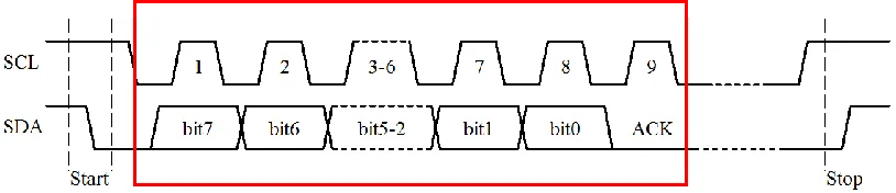
stop signal
When the data transmission is complete, the master device will send a stop signal to inform all devices that the communication has ended.
- Specific timing sequence: When the SCL line remains at high level, the SDA line is pulled up from low level, which is the stop signal.
- Function: Informs the slave device that the communication has ended, allowing it to release the bus and prepare for the next transmission.
📌 Analogy: After the teacher has called everyone's name, he says, "Roll call is over. "

That concludes the entire roll call process.
3.2 Validity of Data Transmission
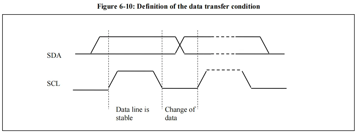
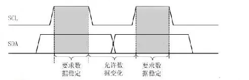
Just as we need to pronounce every word clearly when speaking, it is also necessary to ensure the validity of each bit of data during data transmission. The SDA bus is responsible for transmitting data, and it can only be effectively sampled when the SCL bit is at a stable high level. Therefore, during the high level period of SCL, the data on SDA must remain stable and cannot be changed.
4. Summary of This Chapter
In this chapter, we have systematically got acquainted with I2C (IIC), a very common Communication Protocol in embedded systems, and from the overall picture to specific details, we have gradually understood how it completes multi-device communication with only two wires.
First, starting from the communication model, we clarified that I2C adopts a master-slave architecture. Under this architecture, the master device is responsible for initiating communication and generating clock signals, while the slave device decides whether to respond based on its own address. It is particularly important to note that the identities of "master/slave" and "transmitter/receiver" are not fixed, but dynamically switch as the data direction changes, which also reflects the flexibility of I2C.
Subsequently, we focused on analyzing the physical layer characteristics of I2C. I2C only requires two signal lines, SCL and SDA, to implement synchronous serial communication, which makes it highly suitable for systems with limited pin resources. In this section, we not only learned about the respective functions of the two signal lines, but also gained an in-depth understanding of the "Wired-AND" logic adopted by the I2C bus as well as the open-drain output structure. It is precisely this design that enables multiple devices to safely share the same bus, and also explains why the I2C bus must be externally connected to pull-up resistors to function properly.
On the basis of the physical connection, we further introduce the device address, a core concept. Each I2C slave device has a unique address, and the master device accurately selects the target among numerous slave devices by means of "sending the address first before conducting communication". This process is just like roll call in class: only the device with a matching address will "respond" and thus participate in the subsequent data exchange.
Next, we delved into the protocol layer of I2C, where the actual communication takes place. By analyzing the bus timing, we fully sorted out the three key stages of I2C communication: the start condition, data transmission, and the stop condition. As you have learned, the start and stop conditions are not arbitrary level changes, but rather well-defined timing markers formed when the SDA line undergoes a specific direction transition while SCL is at a high level. It is these strict timing rules that ensure all devices on the bus can correctly recognize the start and end of a communication.
During the data transmission phase, we emphasized two key points: first, data can only be changed when SCL is low, and is sampled when SCL is high; second, after every 8 bits of data, there must be 1 acknowledge bit (ACK / NACK). This structure of "8 data bits + 1 acknowledge bit" is a critical mechanism for I2C to ensure communication reliability, and also provides a clear feedback signal for the coordination between master and slave devices.
Finally, through the analysis of "data transmission validity", we have further reinforced a core principle: data is meaningful only on the premise of a stable clock. This is also the fundamental idea that all synchronous Communication Protocols follow in common.
By studying this chapter, you have built up a comprehensive cognitive framework for I2C communication: why it only requires two wires, why multiple devices can be connected to it in parallel, how data flows step by step on the bus, and the meaning behind every voltage level change. In the following chapters, we will build on these principles, combine the I2C peripheral of ESP32 with specific devices (such as sensors, display modules, etc.), and truly enter the practical stage of "being usable, knowing how to use, and using correctly".