Contents
- I. Module Introduction
- II. Introduction to Major Chips
- 2.1 Chip Overview
- 2.2 Pin Definition
- 2.3 Functional Block Diagram
- 2.4 Performance Parameters
- 2.5 Reference Circuit
- 2.6 Chip Configuration
- 2.7 Communication Interfaces and Related Protocols
- 2.8 PCB Routing Precautions
- III. Circuit Source Engineering and Module Usage Instructions
- 3.1 Circuit Source Engineering
- 3.2 Module Usage Instructions
- 3.3 Application Experiment
- IV. Drivers
- 5. BOM & Recommended Alternative Parts
- VI. Revision History
- VII. Relevant Materials
- 7.1 Chip Datasheet
- 7.2 Unique Icons for PCB Silkscreen
I. Module Introduction
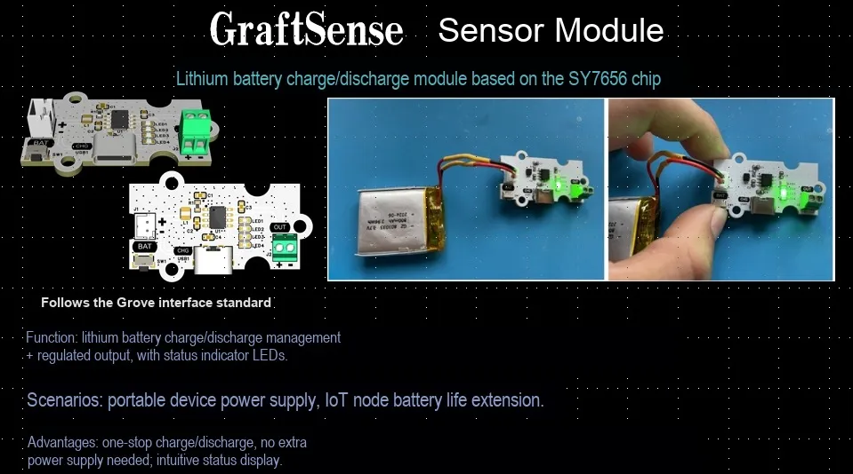
The lithium battery charge-discharge module based on the SY7656 chip is an integrated charge-discharge management chip specifically designed for small-capacity lithium batteries, featuring button control (single-click to start/step-up) and 4-level LED power indication. Its core functions include:
- Charge Management: Supports 1.0A linear charging, features a three-stage process of trickle current / constant current / constant voltage, with a float charge voltage of 4.2V (±1% accuracy), and intelligent over-temperature current derating (starts at 100°C, shuts down at 140°C);
- Boost Discharge: Synchronously outputs 5.1V/1.0A with an efficiency of up to 92%(at a switching frequency of 1MHz), and supports simultaneous charging and discharging;
- Intelligent Control: Automatic output shutdown under light load (continuous <10mA for 16s); locked under undervoltage(
VBAT<2.9V) and requires charging or key unlocking to resume; - Multiple protections: overcurrent, short circuit, overvoltage, overtemperature (150℃ hiccup protection) and reverse current prevention;
- Application Scenarios: Portable devices (Bluetooth earphones, smartwatches), small-capacity power banks and IoT devices, operating temperature: -20℃ to 85℃(ESOP8 package).
II. Introduction to Major Chips
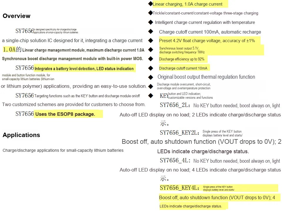
The chip SY7656 adopts the ESOP8 package.
2.1 Chip Overview
2.2 Pin Definition
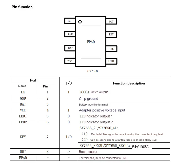
2.3 Functional Block Diagram
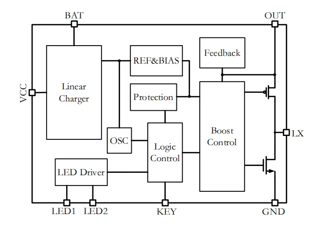
The following is SY7656 an interpretation of the functions of each module in the functional block diagram of the lithium battery charge and discharge management chip, along with an explanation of its working principle combined with typical scenarios:
2.3.1 Power Interface and Energy Conversion
BATInterface: The positive electrode interface of the battery, which connects to a lithium battery (lithium-ion / lithium polymer), provides input energy for the chip's discharge module and simultaneously receives the charging current from the charging module.VCCInterface: Adapter voltage input terminal (2.9V-5.5V), which supplies power to the charging module and triggers the start of the charging function.LXPin: BOOST switch output terminal, connected to an external inductor (L1), which cooperates with the internal power MOS to realize high-frequency (1MHz) boost conversion, converting the battery voltage (2.9V-4.35V) into a 5.1V output.OUTInterface: Step-up output terminal, which outputs a stable 5.1V voltage (with a maximum current of 1.0A) to supply power to external loads.
2.3.2 Core Charge-Discharge Module
Linear Charger(Linear Charging Module): Receives the voltage input fromVCCterminal, and charges the lithium battery at theBATterminal following the three-stage charging logic of "trickle charge - constant current - constant voltage":- When the battery voltage is < 2.9V, trickle pre-charge is performed at a typical current of 100mA;
- When the voltage is >2.9V, switch to 1.0A constant current charging;
- When the voltage approaches 4.2V (float charge voltage), the charger enters constant voltage mode and stops charging until the current drops to 100mA (charge termination current).
- It also features intelligent temperature adjustment function: when the chip junction temperature exceeds 100℃, it will automatically reduce the charging current to avoid damage caused by overheating.
Boost Control(Synchronous Boost Discharge Module): Powered byBAT, it achieves voltage boosting via the high-frequency switch (1MHz) at theLXpin and an external inductor, outputs a 5.1V voltage to theOUTpin, with an efficiency of up to 92%. It supports "charging while discharging": whenVCCand the load are connected simultaneously and the battery voltage is >3.2V, it can charge the battery and supply power to the load at the same time.
2.3.3 Control and Feedback Unit
Logic Control(Control Logic Unit): the "brain" of the chip, responsible for coordinating the operation of all modules:- Receive status signals from the charging module and discharging module (such as battery voltage, output current);
- Responds
to KEYkey input (KEYversion), to control the start/stop of the boost output or the power display; - Switch the charge-discharge mode according to the feedback signal (e. g., automatically enter standby after charging is completed, trigger
LEDturn-off or output turn-off under light load).
Feedback(feedback circuit): Monitors in real timethe battery voltage at the BATpin and the output voltage at theOUTpin, and transmits the signals to the control logic unit to regulate the charging voltage (maintaining an accuracy of 4.2V ±1%) and the discharging voltage (stabilizing the 5.1V output).REF&BIAS(Reference and Bias Circuit): Provides stable reference voltages (e. g., 4.2V charging reference, 5.1V discharging reference) to ensure the accuracy of charging and discharging voltages.
2.3.4 Protection Module
Protection (protection circuit) is used to monitor abnormal conditions and trigger protection actions:
- Overcurrent / Short-circuit Protection: When the current at the
OUTterminal exceeds 2.0A or a short circuit occurs, theBoostoutput will be turned off and restart after 200ms (hiccup mode) until the fault is cleared; - Over temperature protection: The output is shut down when the chip junction temperature exceeds 150°C, and resumes when the temperature drops to 130°C (150°C with 20°C hysteresis);
- Undervoltage protection: When the battery voltage is lower than 2.9V, the Boost output will be locked, which can be unlocked by charging or pressing the KEY button (KEY-equipped version only).
2.3.5 Human-Machine Interaction Interface
KEY: Key input pin (valid only forSY7656_KEY2L/KEY4Lversions):- Click to turn on/off
Boostoutput and check the battery level (triggersLEDdisplay for 16s); - When the battery is in under-voltage lockout mode, click to unlock
Boostoutput (battery voltage > 3.2V required).
- Click to turn on/off
LED1,LED2(indicator light driving terminals): Control the display status of external LEDs:- During charging:
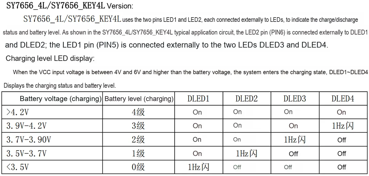
LED2(for the 2-LED version) or multipleLEDs(for the 4-LED version) will flash at 1Hz (when charging) or stay steadily on (when fully charged); - During discharge:
LED1(for the 2-LED version) or multipleLEDs(for the 4-LED version) will remain steadily on (when battery level is sufficient) or flash (for low-battery alarm at a voltage of 2.9V to 3.2V); - In case of abnormality:
LEDsall turn off.
- During charging:
2.3.6 Typical Scenarios
- Startup Output:
- When the user clicks the
KEYkey - The control logic unit receives the signal
- Start
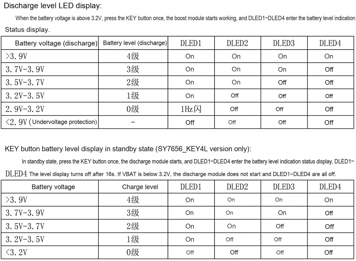
BoostModule LXterminal steps up voltage via an inductorOUTterminal outputs 5.1V to the load, and at the same time,LED1-LED4display the battery level according to the battery voltage (e. g., all 4 LEDs are on when the voltage is above 3.9V).
- When the user clicks the
- Normal Discharge:
FeedbackmonitorsOUTvoltage and battery voltage- The control logic maintains a 5.1V output
- If the load current is <10mA and lasts for 16s, it will automatically turn off
Boost,OUTvoltage drops to 0V, andLEDturns off.
- If the load current is <10mA and lasts for 16s, it will automatically turn off
- Low Battery Protection:
- When the battery voltage drops to 2.9V-3.2V
- The control logic triggers
LED1to blink at 1Hz (low battery alarm)- When the voltage is < 2.9V, the output will be locked
Boostoutput,with allLEDs off; charging or pressing theKEYbutton is required to unlock.
- When the voltage is < 2.9V, the output will be locked
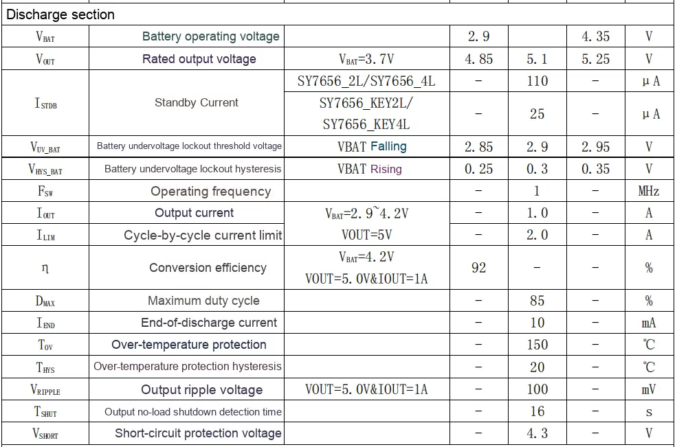
2.4 Performance Parameters
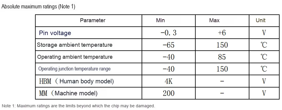
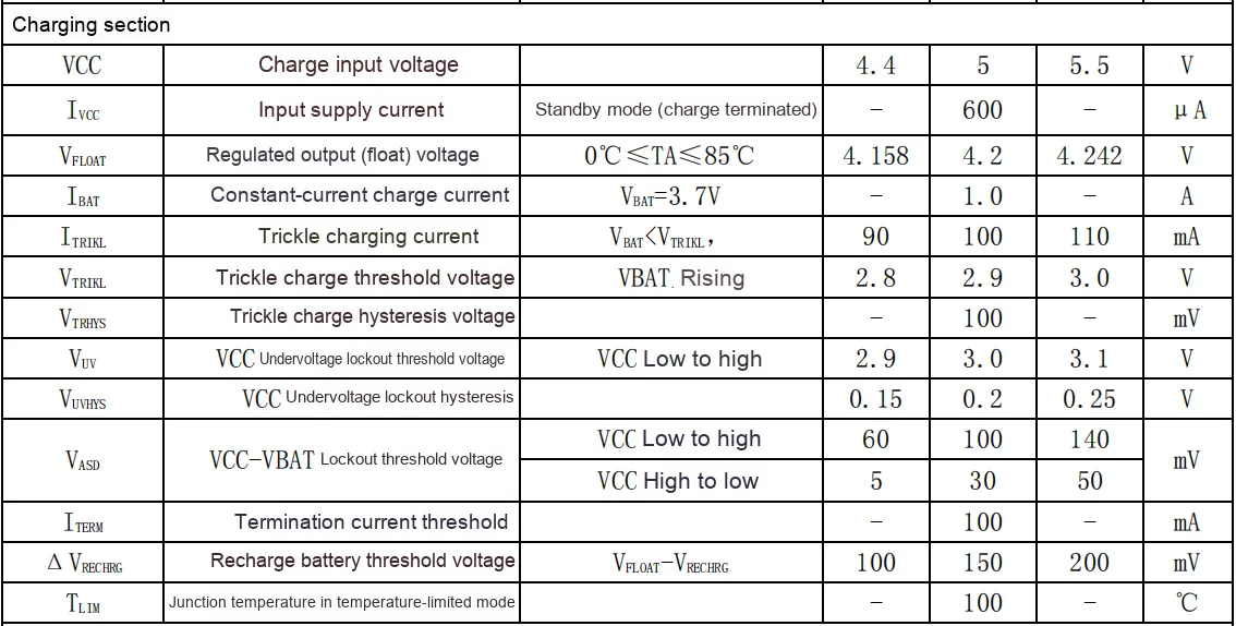

2.5 Reference Circuit
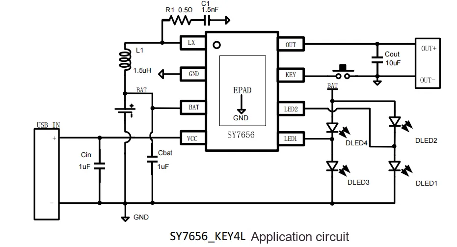
The functions of each component are introduced below by functional circuit category:
2.5.1 Current Detection and Filtering Circuit
R1(0.5Ω): Charging current detection resistor. The linear charging module inside the chip monitors the voltage drop across both ends ofR1(according to Ohm's lawU= IR) to sample the charging current, thereby adjusting the charging current (e. g., maintaining a 1.0 A current during the constant-current charging phase). Meanwhile, in coordination with the protection circuit, it triggers overcurrent protection when the current is abnormally excessive.C1(1.5nF): Forms anR1-RCfilter circuit together with R1. It filters the signal obtained from sampling the internal charging current of the chip, eliminates high-frequency noise interference, makes the detection of charging current more accurate, and ensures that the charging module can stably control the charging current (e. g., 1.0A precision control in the constant current phase). Calculated via the formulafc= 2πRC1, it can filter out interference above a specific frequency and retain the effective charging current signal.
2.5.2 Input Capacitance Filter Circuit
Cin(1μF, X5R material): Input filter capacitor. Connected between the adapter input (VCC) and ground, it is used to filter out high-frequency noise and voltage ripple from the VCC input (such as the ripple output by the adapter), provide a stable operating voltage for the chip's charging module, and prevent voltage fluctuations from affecting charging accuracy (e. g., ±1% accuracy of the 4.2V floating charge voltage). The selection ofX5Rmaterial is due to its excellent capacitance stability over a wide temperature range (−55°C to 85°C), which adapts to the chip's operating environment.
2.5.3 Output Capacitor Filter Circuit
Cout(10μF, X5R material): Output filter capacitor. Connected between the boost output (OUT) and ground, it is used to smooth the high-frequency ripple output by the boost module and ensure a stable 5.1V voltage supplied to the load. Meanwhile, by utilizing the energy storage characteristic of the capacitor, it mitigates the impact of instantaneous load current changes on the output voltage and improves discharge stability.
2.5.4 Battery-side Capacitor Circuit
Cbat(1μF, X5R material): Battery-side filter capacitor. Connected between the battery positive terminal (BAT) and ground, it is used to absorb sudden voltage changes during battery charging and discharging (such as the instantaneous voltage drop during high-current charging/discharging), protect the battery, and meanwhile reduce the interference of voltage fluctuations on the chip's detection circuit (e. g., detection of the 2.9V battery undervoltage lockout threshold) to ensure detection accuracy.
2.5.5 Boost Energy Storage Circuit
L1(1.5μH): Step-up energy storage inductor. In the synchronous step-up discharge module, it cooperates with the on-chip powerMOSto realize energy storage and release based on a 1MHz switching frequency: when the switch is turned on, the inductor stores electrical energy; when the switch is turned off, the inductor releases energy and supplies power to the load through the diode integrated inside the chip, and finally steps up the battery voltage (2.9−4.35V) to 5.1V for output, making it the core energy storage component for the step-up function.
2.5.6 LED Control Circuit
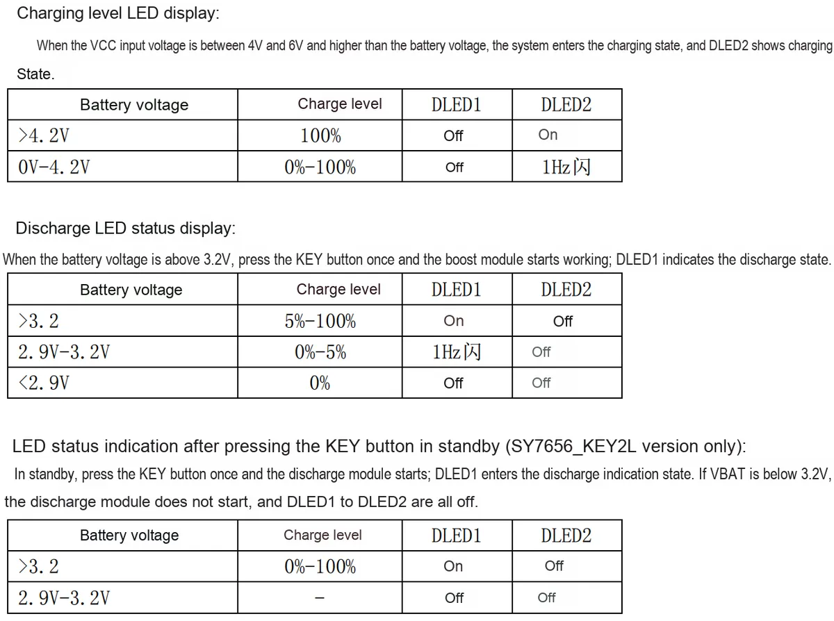
DLED1−DLED4: Status indicatorLED, connected to the chip via theLED1andLED2pins, and controlled by the internal LED driver module of the chip:- During charging, the battery level is displayed in stages based on the battery voltage (e. g., all indicator lights are on when the voltage is >4.2V, and some lights flash when the voltage is <3.5V);
- During discharge, the battery level is indicated by the battery voltage (e. g., all indicator lights are on when the voltage is >3.9V, and some indicator lights are on when the voltage is 3.2−3.5V);
- When the battery is low or an abnormality occurs, the corresponding LED will flash or turn off completely (for example, some LEDs flash when the voltage is between 2.9V and 3.2V), which enables human-machine interaction and intuitively displays the battery status.
2.5.7 Key Control Circuit
KEYUser Interaction Button: Sends a signal to the chip when clicked, thereby triggering the chip to execute the corresponding function:- Turn on / off the boost output, and control
OUTterminal voltage to switch between 5.1V and 0V; - Check the battery level, trigger
DLED1−DLED4to display the current battery level, which will turn off after lasting for 16 seconds; - Unlock battery undervoltage lockout: when the battery voltage is lower than 2.9V, press
KEYto release the boost module lock (normal output is only available after the battery voltage recovers to above 3.2V).
- Turn on / off the boost output, and control
2.5.8 Thermal Pad
EPADThermal Pad: It needs to be connected to the system ground (GND), and the heat dissipation area is expanded through thePCBcopper pour to conduct the heat generated by the chip during high-current charging and discharging (such as 1.0A charging/discharging), prevent the chip junction temperature from exceeding 150°C (the over temperature protection threshold), reduce protection actions caused by overheating (such as hiccup mode), and improve system reliability.
2.6 Chip Configuration
This chip has no relevant configuration information. However, it should be noted that this chip is available in the following four models:
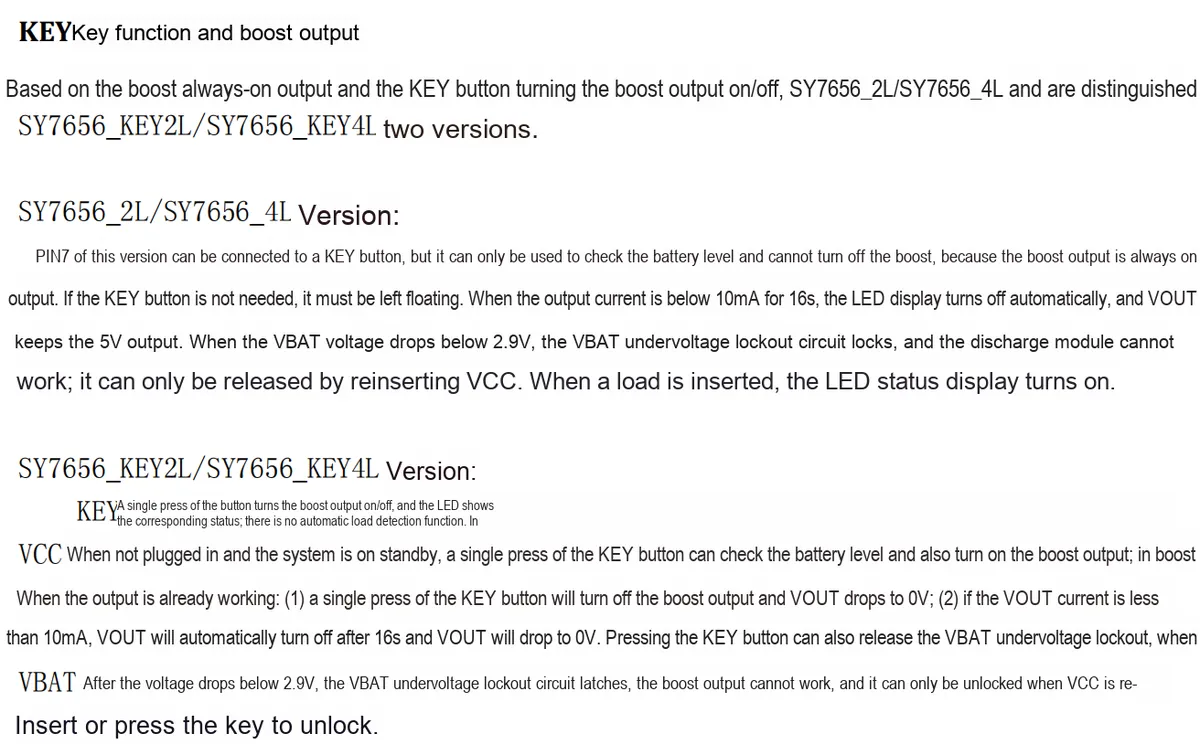
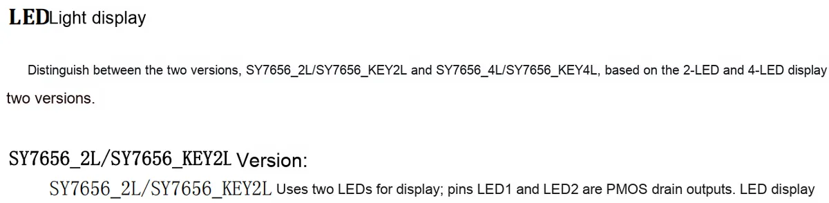
SY7656_2L: No KEY connection required; constant boost output, LED display automatically turns off under light load; 2 LEDs indicate charge/discharge status.SY7656_KEY2L: Press the KEY button to check the battery level and toggle the boost function; it features an auto power-off function (triggered when VOUT drops to 0V) and is equipped with 2 LEDs for charge/discharge status indication.SY7656_4L: No KEY connection required, constant boost output, LED display automatically turns off under light load; 4 LEDs indicate charge/discharge status.SY7656_KEY4L: Press the KEY button to display the battery level and activate/deactivate the boost function as well as the auto power-off function (triggered when VOUT drops to 0V); 4 LEDs are provided for charge/discharge status indication.
The application circuits of the four models are different from one another:
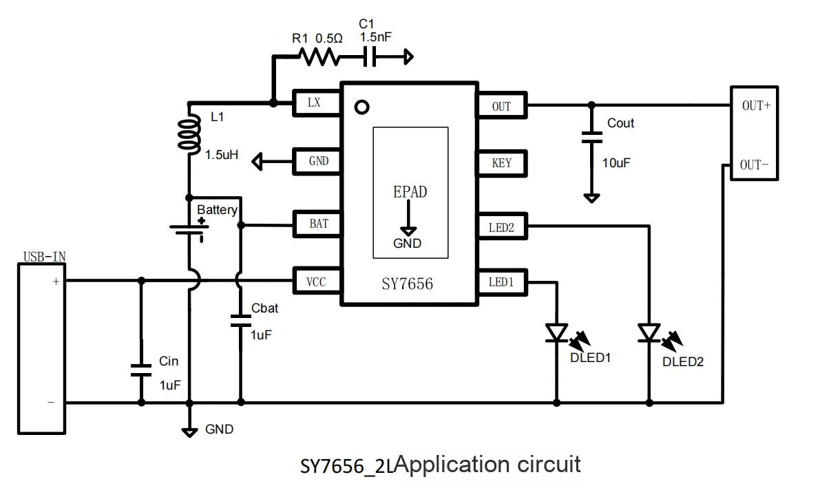
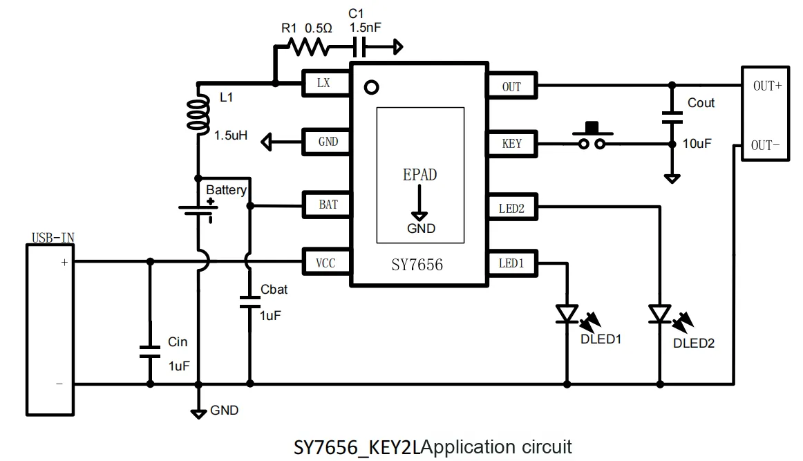
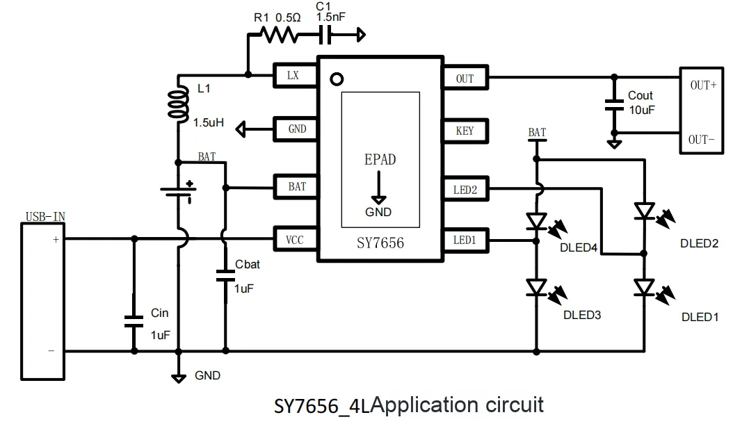
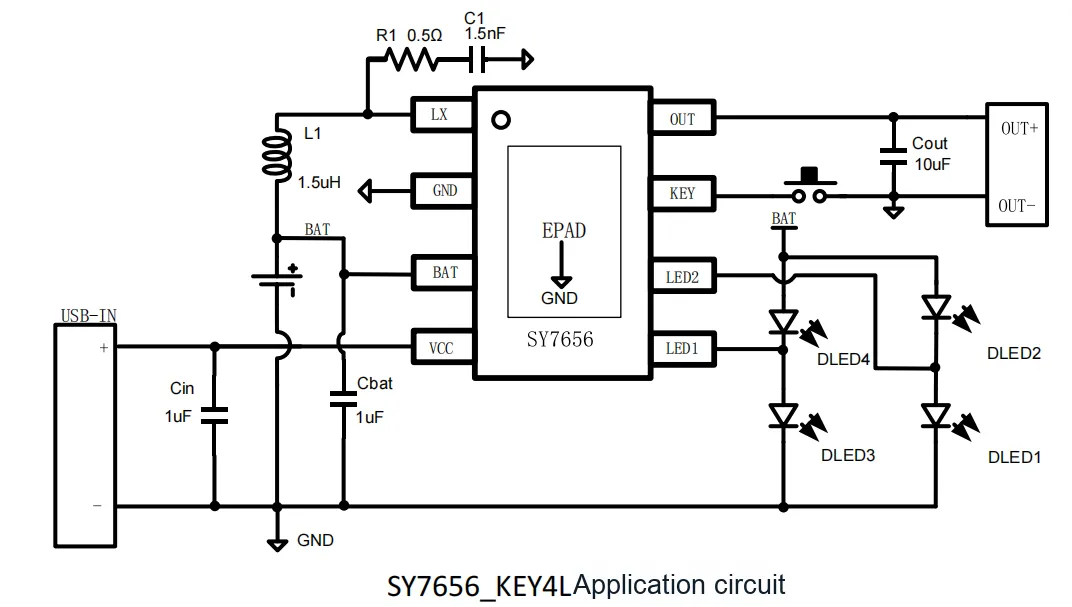
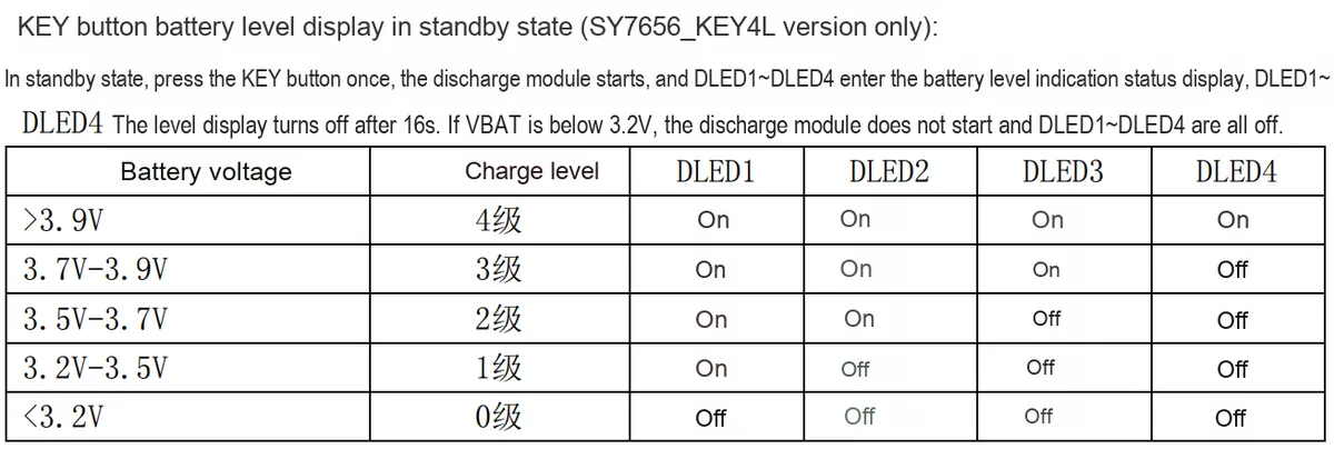
Different types of chips key function and boost output and LED light display are different :

2.7 Communication Interfaces and Related Protocols
No communication interface.
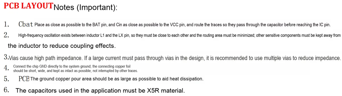
2.8 PCB Routing Precautions
III. Circuit Source Engineering and Module Usage Instructions
3.1 Circuit Source Engineering
To obtain the source project of the circuit, please follow the official account [Freak Embedded]
3.2 Module Usage Instructions
This module adopts SY7656_KEY4L chip, and the reference circuit diagram is shown as follows:
SCH_SY7656-Based Lithium Battery Charge/Discharge Module_v1.1_2025-09-15.pdf 2.3 MB
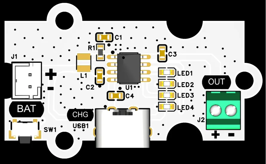
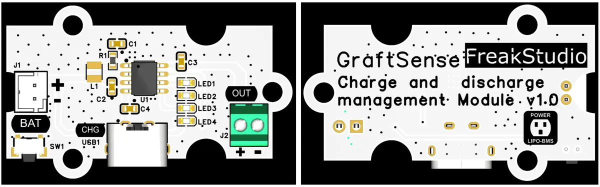
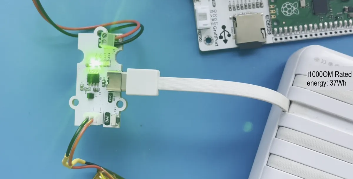
Among them, the BAT interface is connected to a 3.7V polymer lithium battery, the CHG interface is charged via a Type-C interface charging cable, the OUT interface outputs a voltage of 5V, and pressing the SW1 button allows you to check the battery level (which triggers the LED to display for 16 seconds).
For other information, please refer to:
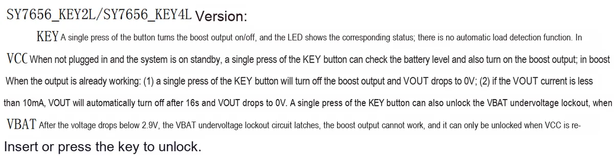
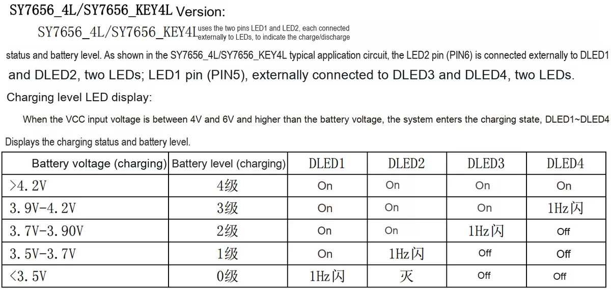
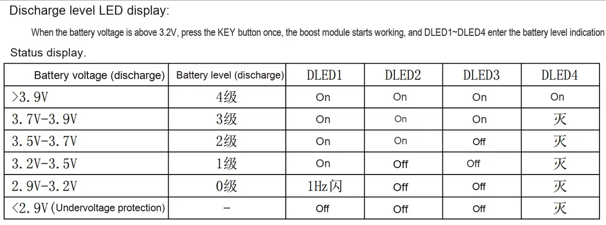
3.3 Application Experiment
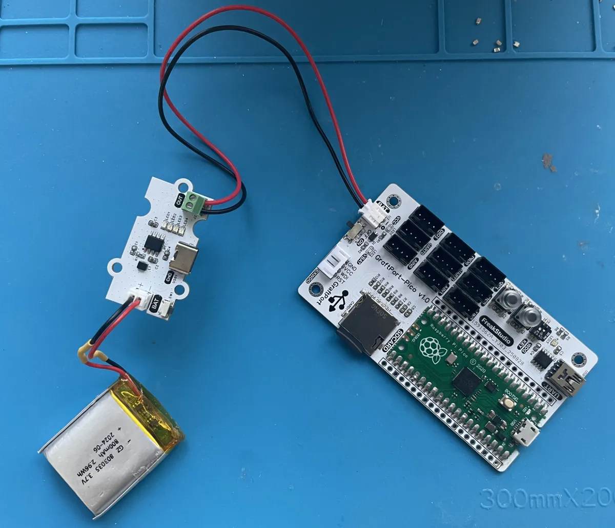
Next, we connect the polymer lithium battery to the BAT interface, and connect the power output OUT terminal to the GraftPort-Rp2040 development board via a PH2.0-2P wire
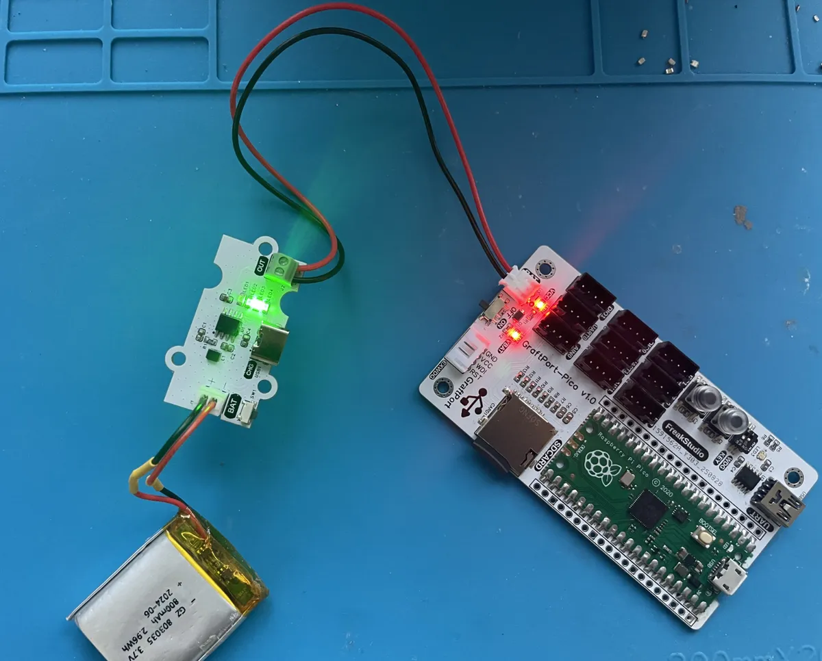
When you flip the switch next to the VBAT interface on the GraftPort-Rp2040 development board, you will see the indicator light on the lithium battery charge-discharge module turn on:
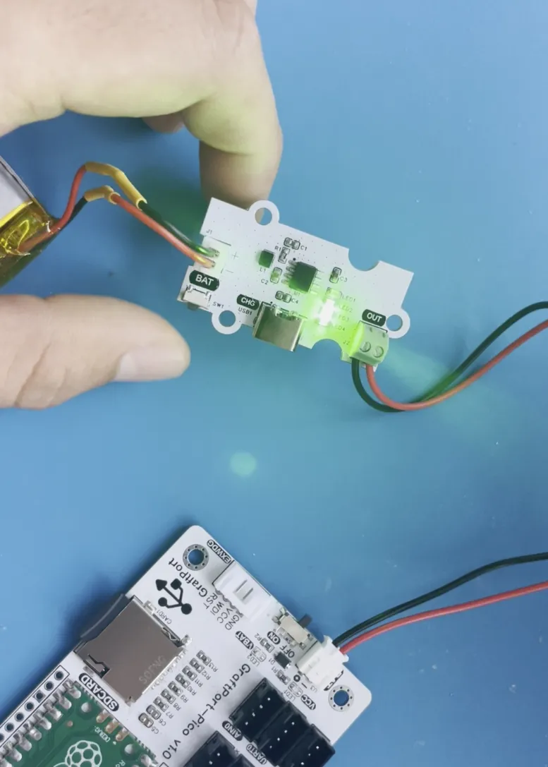
After turning off the switch next to the VBAT interface on the GraftPort-Rp2040 development board and waiting for a while, the lithium battery charge-discharge module enters standby mode, and all LED indicators on it turn off. At this point, pressing the SW1 button on the lithium battery charge-discharge module will display the current power level, and the power display LED will automatically turn off after 16 seconds:
When charging via the Type-C charging cable connected to the CHG port, you will observe the LED indicator flashing:
IV. Drivers
This module does not require driver code.
5. BOM & Recommended Alternative Parts
None.
VI. Revision History
Document Version | Date of Modification | Modifier | Modified Content |
v1.0 | 2025-08-14 | Ling Gaoxing | Complete the initial version of the schematic diagram and PCB design |
v1.1 | 2025-09-15 | Li Zisheng | Revised the document content and optimized the formatting. It is necessary to modify the model of the SY7656 chip; the SY7656_KEY4L should be used, and the BOM list needs to be revised accordingly. At the same time, the directory has been modified. 3.3 Application Experiment Section to be Completed |
v1.2 | 2025-09-15 | Li Zisheng | The application experiment section has been supplemented |
v1.3 | 2025-12-29 | Li Zisheng | Added application experiments and production files |
v1.4 | 2025-12-31 | Xin Ruili | Create an open version of the document, based on the internal document version v1.3. |
VII. Relevant Materials
7.1 Chip Datasheet
SY7656-V1.0.PDF 702 KB
7.2 Unique Icons for PCB Silkscreen