Contents
- I. Module Introduction
- II. Introduction to Main Chips
- 2.1 Chip Overview
- 2.2 Pin Definition
- 2.3 Functional Block Diagram
- 2.4 Performance Parameters
- 2.5 Reference Circuit
- 2.6 Chip Configuration
- 2.7 Communication Interfaces and Related Protocols
- 2.8 PCB Routing Precautions
- III. Circuit Engineering
- 3.1 Circuit Source Engineering
- 3.2 Module Usage Instructions
- 3.3 Application Experiment
- IV. Drivers
- 5. BOM & Recommended Alternative Parts
- VI. Revision History
- VII. Relevant Materials
- 7.1 Chip Datasheet
- 7.2 Unique Icons for PCB Silk Screen
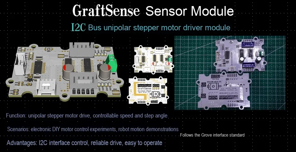
I. Module Introduction
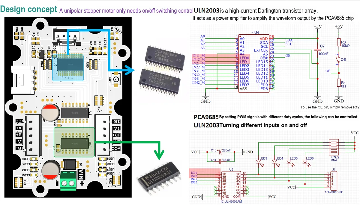
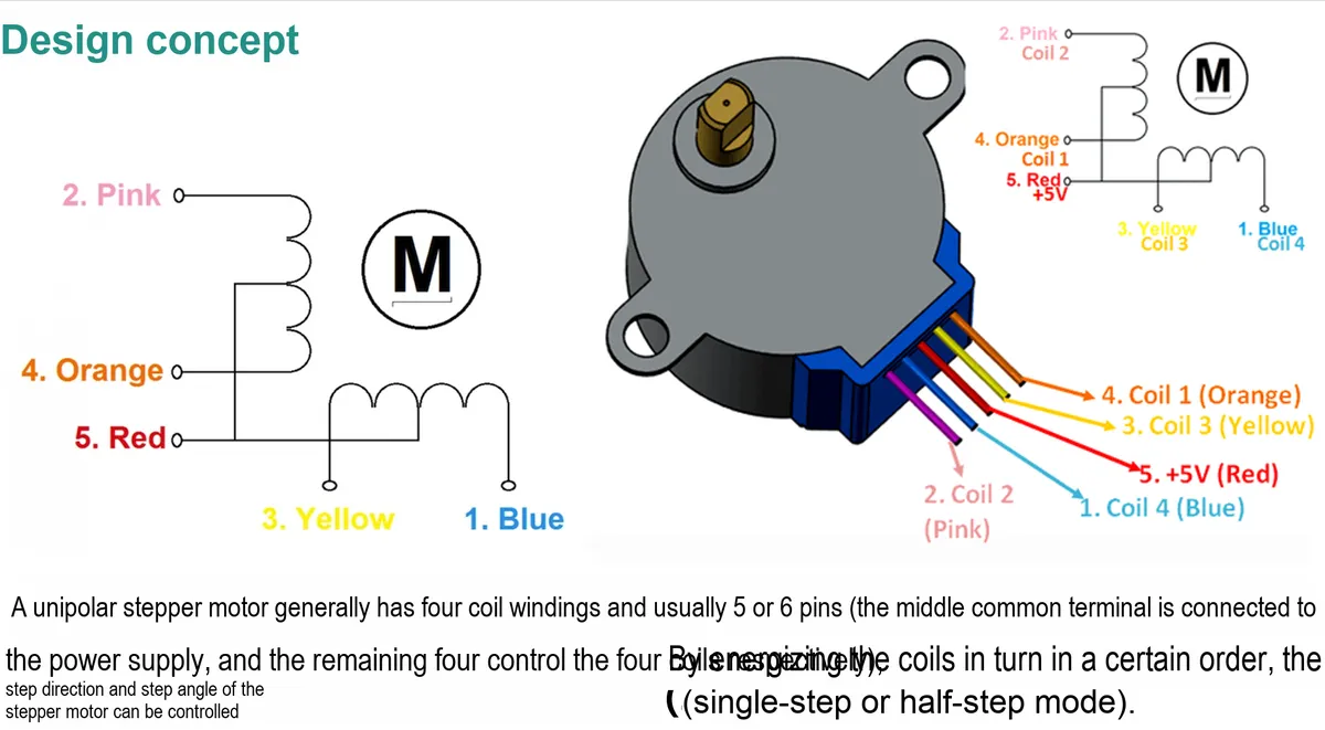
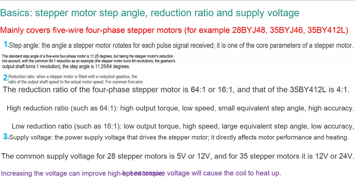
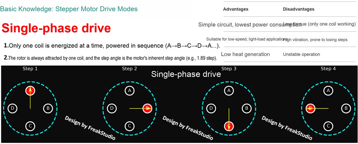
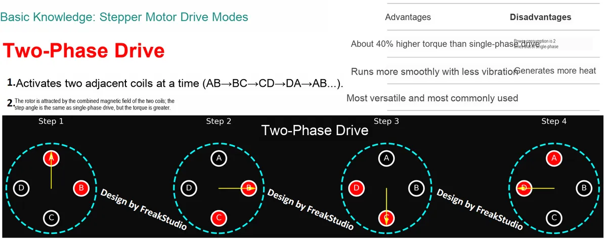
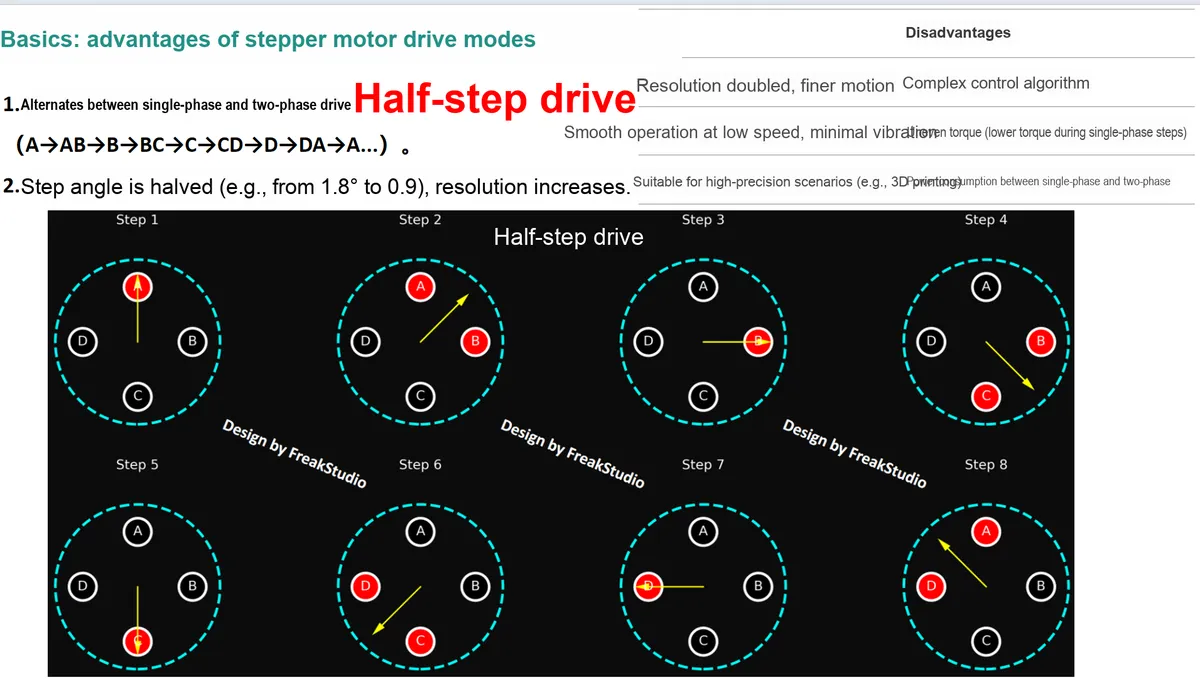
I2C Bus Unipolar Stepper Motor Driver Module, which is controlled via the I2C interface and features designs such as address selection control and pin current limiting protection. The module can output a maximum current of 8A, supports single-step, full-step and half-step driving modes, is specially designed for 5-wire unipolar stepper motors (such as 28BYJ-48), can drive 2 stepper motors, and is equipped with circuits including motor power supply input, stepper motor drive unit, power filtering and power indicator.It is applicable to unipolar stepper motor control scenarios such as automated equipment and 3D printing, and provides the system with an efficient stepper motor drive solution based on the I2C bus.
II. Introduction to Main Chips
This module mainly uses the PCA9685PW, 118 PWM control chip and the ULN2003AM/TR motor driver chip, and their related introductions are as follows:
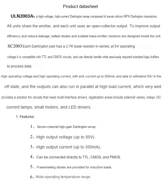
ULN2003AM/TR is a high-voltage-tolerant and high-current 7-channel Darlington transistor array chip, with a rated output current of 500mA per channel, a peak current of up to 600mA, can withstand a high voltage of 50V in the off state, and has a built-in freewheeling clamp diode that can suppress the back EMF of inductive loads.Its input is directly compatible with 5V TTL and CMOS logic circuits without requiring additional buffers, operates over a temperature range of -40°C to 105°C, and is available in packages including DIP-16 and SOP-16. It supports channel parallel connection to increase output current, complies with the ROHS directive, and is commonly used to drive loads such as stepper motors, relays and LEDs, being widely applied in microcontroller control systems, automation equipment and various industrial control scenarios.
PCA9685PW, 118 is a 16-channel 12-bit high-precision PWM control chip. It communicates via I²C bus, has a built-in 25MHz oscillator, with programmable PWM frequency ranging from 24Hz to 1526Hz; the 12-bit resolution enables fine control of 4096 levels, and each channel has a maximum output current of 25mA and can be configured independently.This chip supports 64 different address configurations, allows up to 8 devices to be cascaded for channel expansion, features a standby current of less than 10μA with extremely low power consumption, and also boasts glitch-free output upon power-up, hot-swappable and other characteristics. It can not only drive LEDs for backlight dimming but also precisely control steering gears, and is widely used in multi-channel PWM control scenarios such as robots, smart homes, and drones.
2.1 Chip Overview
2.1.1 Overview of ULN2003AM/TR
2.1.2 Overview of PCA9685PW, 118
The PCA9685 is a 16-channel LED controller controlled via the I²C bus, optimized for RGBA color backlighting, with each output featuring a 12-bit PWM controller, adjustable frequency ranging from 24 to 1526 Hz and duty cycle from 0 to 100%, and all outputs operate at the same PWM frequency.
The output can be configured to off, on, or custom PWM dimming; the pole can be set to open-drain (sink 25mA) or totem-pole (sink 25mA, source 10mA @5V); it operates at a supply voltage of 2.3 - 5.5V, with I/O pins tolerant to 5.5V, and LEDs can be connected directly or via an external driver.
It belongs to the Fm+ series, supports 1MHz communication and high bus load, and features unique characteristics compared with PCA96935, including staggered LED switching time, 4096-level PWM, programmable PWM pulse width, external clock input (up to 50MHz), wider PWM frequency range (24 - 1526Hz), and default low power-on output.
The active-low OE pin enables asynchronous output control; the software-programmable global/child call addresses support synchronous control of multi-device groups; the 6 hardware address pins allow connection of up to 62 devices; the software reset initializes all registers with a single click.
Features and Advantages
- 16-channel LED driver with each channel programmable for off, on, brightness and turn-on time (for EMI reduction)
- 1MHz Fm+ I²C interface, with 30mA high drive capability on SDA, suitable for high-capacitance buses
- 4096 levels (12-bit) linear brightness adjustment, frequency 24 - 1526Hz adjustable
- Totem pole / open-drain output optional (5V, 25mA sink current, 10mA source current), output update timing programmable
- The OE pin supports flexible control over the output state, and the 6 address pins support a shared bus for up to 62 devices
- hardware flashing, multi-group software address addressing, software reset, 25MHz internal oscillator (no external components)
- External 50MHz clock input, power-on reset, noise filtering, edge rate control, and hot-swap support
- Low standby current, operating voltage of 2.3 - 5.5V, operation within -40 ~ + 85℃, excellent ESD protection, and available in TSSOP28/HVQFN28 packages
Application
- RGB/RGBA LED drivers, LED status indication, LED displays
- LCD backlight, keyboard backlight for mobile phones/handheld devices
2.2 Pin Definition
2.2.1 Pin Definition of ULN2003AM/TR
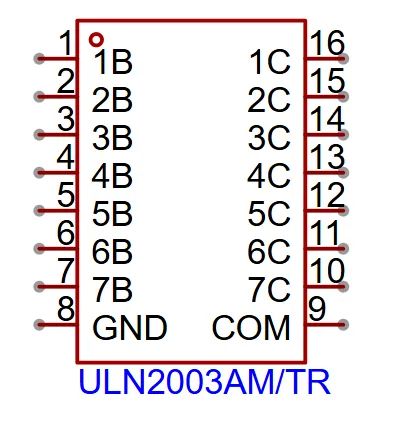
The ULN2003A mostly comes in a DIP-16 package with a total of 16 pins, covering types such as input, output, power supply, ground and common terminal. The detailed description of each pin by number is as follows:
| Pin number | Pin name | Function description |
| 8 | GND | Ground terminal. Connect it to the common ground of the circuit board to give the chip a stable potential reference and ensure normal circuit operation. |
| 1, 7 | 1B - 7B | 7 independent signal inputs, compatible with TTL/CMOS logic levels. Usually connected to a low-current drive source such as a microcontroller. A high-level input (≥2.0V) turns on the corresponding output, and a low-level input (≤0.8V) puts the corresponding output in a high-impedance state. Each input corresponds to one driver channel. |
| 9 | COM | Chip operating power supply input, which powers the internal bias circuit and logic input gates. The typical operating voltage is 5V, with a range of usually 4.5V - 25V. It can be set separately from the supply of the driven load. |
| 10, 16 | 1C- 7C | 7-channel open-collector outputs, corresponding one-to-one with IN1 - IN7. When the input is high, the corresponding output turns on and pulls to ground (outputs low); when the input is low, the output turns off and is high-impedance. In practice, one end of the load connects to the output and the other end to the positive supply provided at COM; each channel can withstand a maximum continuous current of 500mA. |
2.2.2 PCA9685PW, 118 Pin Definition
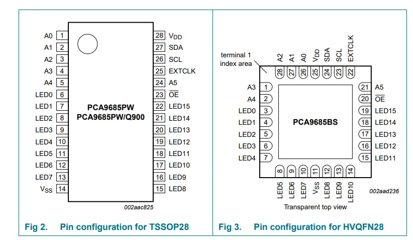
| Symbol | TSSOP28 Pin | HVQFN28 Pin | Type | Description |
| A0 | 1 | 26 | Input | Address Input 0 |
| A1 | 2 | 27 | Input | Address Input 1 |
| A2 | 3 | 28 | Input | Address Input 2 |
| A3 | 4 | 1 | Input | Address Input 3 |
| A4 | 5 | 2 | Input | Address Input 4 |
| LED0 | 6 | 3 | Output | LED Driver 0 |
| LED1 | 7 | 4 | Output | LED Driver 1 |
| LED2 | 8 | 5 | Output | LED Driver 2 |
| LED3 | 9 | 6 | Output | LED Driver 3 |
| LED4 | 10 | 7 | Output | LED Driver 4 |
| LED5 | 11 | 8 | Output | LED Driver 5 |
| LED6 | 12 | 9 | Output | LED driver 6 |
| LED7 | 13 | 10 | Output | LED driver 7 |
| Vss | 14 | 11⁽¹⁾ | Power supply | Power ground |
| LED8 | 15 | 12 | Output | LED driver 8 |
| LED9 | 16 | 13 | Output | LED driver 9 |
| LED10 | 17 | 14 | Output | LED driver 10 |
| LED11 | 18 | 15 | Output | LED driver 11 |
| LED12 | 19 | 16 | Output | LED driver 12 |
| LED13 | 20 | 17 | Output | LED driver 13 |
| LED14 | 21 | 18 | Output | LED driver 14 |
| LED15 | 22 | 19 | Output | LED driver 15 |
| OE | 23 | 20 | Input | Active-low LED output enable |
| A5 | 24 | 21 | Input | Address input 5 |
| EXTCLK | 25 | 22 | Input | External clock input⁽²⁾ |
| SCL | 26 | 23 | Input | Serial clock line |
| SDA | 27 | 24 | Input/output | Serial data line |
| VDD | 28 | 25 | Power supply | Supply voltage |
2.3 Functional Block Diagram
2.3.1 Functional Block Diagram of ULN2003AM/TR
PCA9685PW, 118 has no functional block diagram description, and this chapter only introduces the functional block diagram of ULN2003AM/TR.
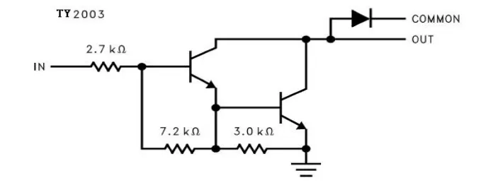
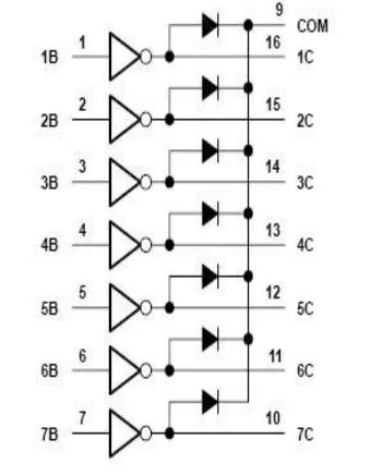
The functional block diagram of ULN2003AM/TR is described as follows.
- Input and Current Limiting Module
- IN (Input Pin): Receives external TTL/CMOS logic level signals.
- 2.7kΩ resistor: It limits the input current to protect the internal transistors, and meanwhile provides an appropriate bias current for the base.
- Amplification and Driving Module
- Darlington transistor pair: Consists of two transistors, which realizes the current amplification function and amplifies the input small current signal into a large current signal sufficient to drive a heavy load.
- 7.2kΩ and 3.0kΩ resistors: provide biasing and feedback for the Darlington transistor pair, stabilize the operating point of the transistors, and ensure amplification performance.
- Output and Protection Module
- OUT (Output Pin): Open-collector output terminal, capable of driving high-current loads.
- Freewheeling diode: Cooperating with the output terminal, it feeds back the back electromotive force generated when the inductive load is powered off, so as to protect the internal Darlington transistor from breakdown.
- COMMON: When driving an inductive load, connect it to the positive power supply of the load to serve as the common cathode of the freewheeling diodes; when driving a resistive load, it can be left floating or connected to VCC.
2.4 Performance Parameters
2.4.1 Performance Parameters of ULN2003AM/TR
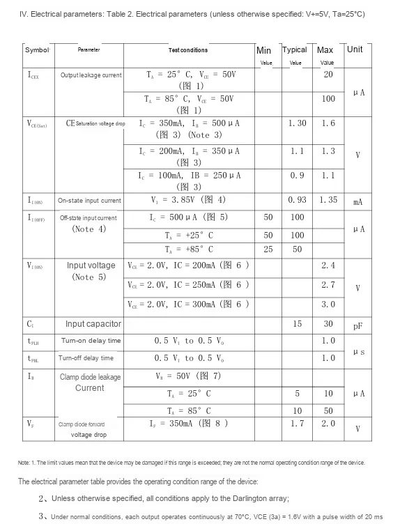
ULN2003AM/TR has the following electrical characteristic parameters:
- The maximum leakage current of the output tube is 20μA (at 25℃) and 100μA (at 85℃);
- Minimum CE saturation voltage drop: 1.1V (under different current conditions);
- ON-state input current typically 0.93mA, maximum 1.35mA;
- Off-state input current max. 100μA;
- Input voltage max. 3.0V;
- Input capacitance: typically 15 pF, maximum 30 pF;
- Turn-on / Turn-off Delay Time Max. 1.0μs;
- Freewheeling diode leakage current: max. 10μA (at 25℃), 50μA (at 85℃);forward voltage drop: typical 1.7V, max. 2.0V.
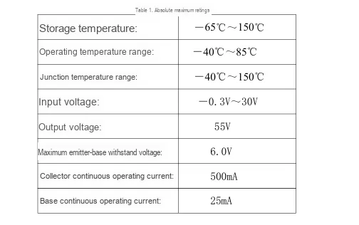
ULN2003AM/TR Some of its absolute maximum parameters are as follows:
- Storage temperature: -65~150℃, Operating temperature: -40~85℃, Junction temperature: -40~150℃;
- Input voltage: 0.3~30V, Output voltage: max. 55V;
- Maximum emitter-base voltage 6.0 V, Continuous collector current 500 mA, Continuous base current 25 mA.
2.4.2 Performance Parameters of PCA9685PW, 118
The absolute maximum ratings of PCA9685PW, 118 are as follows:
| Symbol | Parameter | Conditions | Min | Max | Unit |
| VDD | Supply voltage | - | -0.5 | 6 | V |
| VIO | Input/output pin voltage | - | VSS−0.5 | 5.5 | V |
| IO(EDn) | LEDn pin output current | - | - | 25 | mA |
| ISS | Ground supply current | - | - | 400 | mA |
| Ptot | Total power dissipation | - | - | 400 | mW |
| Tstg | Storage temperature | - | -65 | 150 | °C |
| Tamb | Ambient temperature | Operating state | -40 | 85 | °C |
The static parameters of PCA9685PW, 118 are as follows:(V DD = 2.3 V to 5.5 V; V SS = 0 V; unless otherwise specified)
| Symbol | Parameter | Conditions | Min | Typ | Max | Unit |
| Power supply | - | - | - | - | - | - |
| VDD | Supply voltage | - | 2.3 | - | 5.5 | V |
| IDD | Supply current | Operating mode: no load; fSCL=1MHz; VDD=2.3V to 5.5V | - | 6 | 10 | mA |
| Isb | Standby current | No load; fSCL=0Hz; VI=VDD or VSS; VDD=2.3V to 5.5V | - | 2.2 | 15.5 | μA |
| VPOR | Power-on reset voltage | No load; VI=VDD or VSS | ⁽¹⁾ - | 1.7 | 2 | V |
| Input SCL; input/output SDA | - | - | - | - | - | - |
| VIL | Low-level input voltage | - | -0.5 | - | +0.3VDD | V |
| VIH | High-level input voltage | - | 0.7VDD | - | 5.5 | V |
| IOL | Low-level output current | VOL=0.4V; VDD=2.3V | 20 | 28 | - | mA |
| VOL=0.4V; VDD=5.0V | 30 | 40 | - | mA | ||
| IL | Leakage current | VI=VDD or VSS | -1 | - | 1 | μA |
| Ci | Input capacitance | VI=VSS | - | 6 | 10 | pF |
| LED driver output | - | - | - | - | - | - |
| IOL | Low-level output current | VOL=0.5V; VDD=2.3V to 4.5V | ⁽²⁾ 12 | 25 | - | mA |
| IOL(total) | Total low-level output current | VOL=0.5V; VDD=4.5V | - | - | 400 | mA |
| IOH | High-level output current | Open-drain; VOH=VDD | -10 | - | 10 | μA |
| VOH | High-level output voltage | IOH=−10mA; VDD=3.0V | 1.6 | - | - | V |
| IOH=−10mA; VDD=2.3V | 2.3 | - | - | V | ||
| IOH=−10mA; VDD=4.5V | 4 | - | - | V | ||
| IOZ | Off-state output current | Three-state; VOH=VDD or VSS | -10 | - | 10 | μA |
| Co | Output capacitance | - | - | 5 | 8 | pF |
| VIL | Low-level input voltage | - | -0.5 | - | +0.3VDD | V |
| VIH | High-level input voltage | - | 0.7VDD | - | 5.5 | V |
| II | Input leakage current | - | -1 | - | 1 | μA |
| Ci | Input capacitance | - | - | 3 | 5 | pF |
⁽¹⁾ To reset the device, V DD must be lowered to 0.2 V.
⁽²⁾ Due to internal bus limitations, the maximum current per pin is limited to 25 mA, and the total package current is limited to 400 mA.
The dynamic parameters of PCA9685PW, 118 are as follows: (V DD = 2.3 V to 5.5 V; V SS = 0 V; unless otherwise specified)
| Symbol | Parameter | Conditions | Standard-mode I²C bus | Fast-mode I²C bus | Fast-mode Plus I²C bus | Unit | |||
| Min | Max | Min | Max | Min | Max | - | |||
| fSCL | SCL clock frequency | ⁽¹⁾ | 0 | 100 | 0 | 400 | 0 | 1000 | kHz |
| fEXTCLK | EXTCLK pin frequency | - | DC | 50 | DC | 50 | DC | 50 | MHz |
| tBUF | Bus free time between STOP and START conditions | - | 4.7 | - | 1.3 | - | 0.5 | - | μs |
| tHD:STA | (Repeated) START condition hold time | - | 4 | - | 0.6 | - | 0.26 | - | μs |
| tSU:STA | (Repeated) START condition setup time | - | 4.7 | - | 0.6 | - | 0.26 | - | μs |
| tSU:STO | Stop condition setup time | - | 4 | - | 0.6 | - | 0.26 | - | μs |
| tHD:DAT | Data hold time | - | 0 | - | 0 | - | 0 | - | ns |
| tVD:ACK | Data valid acknowledge time | ⁽²⁾ | 0.3 | 3.45 | 0.1 | 0.9 | 0.05 | 0.45 | μs |
| tVD:DAT | Data valid time | ⁽³⁾ | 0.3 | 3.45 | 0.1 | 0.9 | 0.05 | 0.45 | μs |
| tSU:DAT | Data setup time | - | 250 | - | 100 | - | 50 | - | ns |
| tLOW | SCL clock low period | - | 4.7 | - | 1.3 | - | 0.5 | - | μs |
| tHIGH | SCL clock high period | - | 4 | - | 0.6 | - | 0.26 | - | μs |
| tf | Fall time of SDA and SCL signals | ⁽⁴⁾⁽⁵⁾ | - | 300 | 20 + 0.1Cb⁽⁶⁾ | 300 | - | 120 | ns |
| tr | Rise time of SDA and SCL signals | ⁽⁴⁾⁽⁵⁾ | - | 1000 | 20 + 0.1Cb⁽⁶⁾ | 300 | - | 120 | ns |
| tSP | Pulse width of spikes to be suppressed by the input filter | ⁽⁷⁾ | - | 50 | - | 50 | - | 50 | ns |
| tHZ:L | Low-level to off-state propagation delay | OE to LEDn; OUTNE [1:0] = 10 or 11; MODE2 register | - | 40 | - | 40 | - | 40 | ns |
| tZL:L | Off-state to low-level propagation delay | OE to LEDn; OUTNE [1:0] = 10 or 11; MODE2 register | - | 60 | - | 60 | - | 60 | ns |
| tIH:Z | High-level to off-state propagation delay | OE to LEDn; OUTNE [1:0] = 10 or 11; MODE2 register | - | 60 | - | 60 | - | 60 | ns |
2.5 Reference Circuit
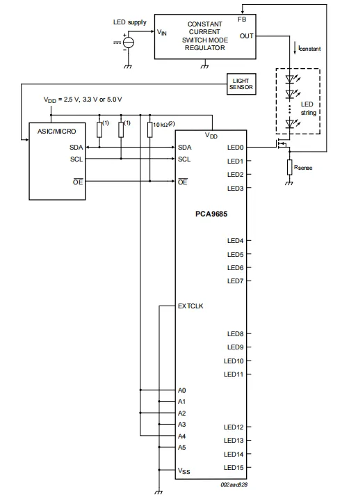
The manufacturer does not provide the reference circuit for ULN2003AM/TR; the following is the reference circuit for PCA9685PW, 118:
2.6 Chip Configuration
ULN2003AM/TR requires no additional configuration in practical applications, PCA9685PW, 118 only needs the IIC address to be selected during application.
2.7 Communication Interfaces and Related Protocols
ULN2003AM/TR does not require protocol communication during application, and this section only introduces PCA9685PW, 118 the IIC communication.
2.7.1 Registers
2.7.1.1 Mode Register 1, MODE1
Table 5: MODE1 - Bit Description Legend for Mode Register 1 (Address 00h): * indicates default value
| Bit | Symbol | Access | Value | Description |
| 7 | RESTART | Read/Write | - | Shows the state of the RESTART logic. The user writes logic 1 to this bit to clear it to logic 0; writing logic 0 has no effect. 0*: RESTART disabled. 1: RESTART enabled. |
| 6 | EXTCLK | Read/Write | - | To use the EXTCLK pin, set this bit with the following steps: 1. Set the EXTCLK bit in MODE1, which turns off the internal oscillator. 2. Write logic 1 to both the SLEEP and EXTCLK bits in MODE1 to complete the switch. The external clock can remain active during the switch because the SLEEP bit is set. This bit is "sticky": writing logic 0 cannot clear it; the EXTCLK bit can only be cleared by a power cycle or software reset. The EXTCLK range is DC to 50 MHz. See the refresh rate formula after the table. 0*: Use internal clock. 1: Use EXTCLK pin clock. |
| 5 | AI | Read/Write | - | 0*: Register auto-increment disabled⁽¹⁾. 1: Register auto-increment enabled. |
| 4 | SLEEP | Read/Write | 0 | Normal mode⁽²⁾. 1*: Low-power mode. Oscillator off⁽³⁽⁴⁾. |
| 3 | SUB1 | Read/Write | 0* | PCA9685 does not respond to I²C-bus subaddress 1. 1: PCA9685 responds to I²C-bus subaddress 1. |
| 2 | SUB2 | Read/Write | 0* | PCA9685 does not respond to I²C-bus subaddress 2. 1: PCA9685 responds to I²C-bus subaddress 2. |
| 1 | SUB3 | Read/Write | 0* | PCA9685 does not respond to I²C-bus subaddress 3. 1: PCA9685 responds to I²C-bus subaddress 3. |
| 0 | ALLCALL | Read/Write | 0 | PCA9685 does not respond to LED All Call I²C-bus address. 1*: PCA9685 responds to LED All Call I²C-bus address. |
Refresh rate formula:

⁽¹⁾ When the auto-increment flag is set (AI = 1), the control register is automatically incremented after each read or write operation, allowing users to program the registers sequentially.
(2) After the SLEEP bit is set to logic 0, the oscillator requires 500 μs to start up and stabilize. If the PWM control register is accessed within this 500 μs window, the timing of the LEDn output is not guaranteed to be stable. When the EXTCLK pin is used as the PWM clock, no start-up delay is required.
(3) PWM control cannot be performed when the oscillator is off.
⁽⁴⁾ When the oscillator is off (in sleep mode), the LEDn output cannot be turned on, turned off, dimmed or flashed.
2.7.1.2 Restart Mode
If the PCA9685 is in operation and the user puts the chip into sleep mode (by setting bit 4 of MODE1) without stopping any PWM channels, the RESTART bit (bit 7 of MODE1) will be set to logic 1 at the end of the PWM refresh cycle. The contents of each PWM register remain valid when the clock is shut down.
To restart all previously active PWM channels with a small number of I²C bus cycles, follow the steps below:
- Read the MODE1 register.
- Check whether bit 7 (RESTART) is logic 1. If yes, clear bit 4 (SLEEP) and wait for the oscillator to stabilize (500 μs).
- Write a logic 1 to bit 7 of the MODE1 register. All PWM channels will be reset, and the RESTART bit will be cleared.
Note: Before writing a logic 1 to the RESTART bit, the SLEEP bit must be held at logic 0 for a minimum of 500 μs.
The following operations will also clear the RESTART bit:
- Power-off cycle.
- I²C software reset command.
- If the OCH bit of the MODE2 register is logic 0, issue an I²C bus STOP command after writing to any PWM register.
- If the OCH bit of the MODE2 register is a logic 1, write to all four PWM registers of any PWM channel.
Similarly, if the user disables all PWM channels out of order before setting the SLEEP bit⁽¹⁾, the RESTART bit will also be cleared. At this point, the contents of all PWM registers become invalid and must be reloaded before being used again.
One application example of the RESTART bit is: when a client's laptop resumes from the standby state, the LCD backlight brightness will be restored to the level it was at before entering standby.
⁽¹⁾ This refers to the operation of not closing all PWM channels in a specific sequence.
2.7.1.3 Mode Register 2, MODE2
Table 6: MODE2 - Bit Description Legend for Mode Register 2 (Address 01h): * indicates default value
| Bit | Symbol | Access | Value | Description |
| 7 to 5 | - | Read-only | 000* | Reserved |
| 4 | INVRT⁽¹⁾ | Read/Write | 0* | Output logic state not inverted. This value is used when an external driver is used; valid when OE=0. 1: Output logic state inverted. This value is used when no external driver is used; valid when OE=0. |
| 3 | OCH | Read/Write | 0* | Outputs change on STOP command⁽²⁾. 1: Outputs change on ACK⁽³⁾. |
| 2 | OUTDRV⁽¹⁾ | Read/Write | 0 | The 16 LEDn outputs are configured with a totem pole structure. 1*: The 16 LEDn outputs are configured with an open-drain structure. |
| 1 to 0 | OUTNE[1:0]⁽⁴⁾ | Read/Write | 00* | When OE=1 (output drivers not enabled), LEDn = 0. 01: When OE=1 (output drivers not enabled): - If OUTDRV = 1, LEDn = 1 - If OUTDRV = 0, LEDn = high-impedance (same as OUTNE [1:0] = 10) 1X: When OE=1 (output drivers not enabled), LEDn = high-impedance. |
⁽¹⁾ Standard LEDs can be directly driven in any mode. Some new-generation LEDs integrate Zener diodes to limit voltage transients, reduce EMI and protect the LEDs, and these LEDs must be driven exclusively in open-drain mode to prevent IC overheating. The default state of the LEDn output pins after power-on reset is low.
⁽²⁾ The output change on the STOP command allows synchronization of outputs from multiple PCA9685 devices. This applies only to registers from 06h (LED0_ON_L) to 45h (LED15_OFF_H).One or more registers can be written in any order before stopping.
⁽³⁾ For the update-on-acknowledgment requirement, all 4 PWM channel registers must be loaded before the last acknowledgment, so that the output will change.
2.7.1.4 LED Output and PWM Control
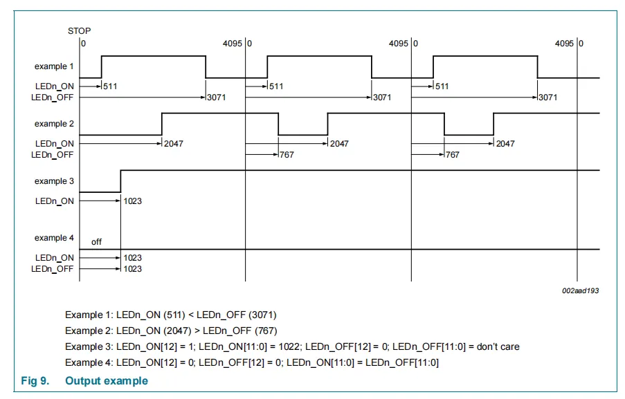
The turn-on time and PWM duty cycle of each LED driver output can be independently controlled via the LEDn_ON and LEDn_OFF registers.
Each LED output has two 12-bit registers that are programmed by the user, with a value range of 0 to 4095. One 12-bit register stores the on-time value, and the other stores the off-time value. The on and off times are compared with the value of a 12-bit counter that runs continuously from 0000h to 0FFFh (decimal 0 to 4095).
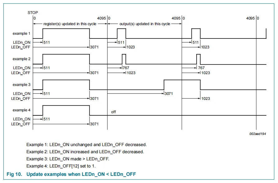
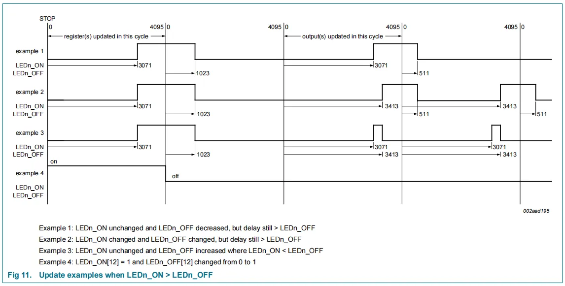
When responding, the update requirement mandates that all 4 PWM channel registers be loaded before the last response, so that the output will change accordingly.
The programmable turn-on time refers to the time when the LED output is set, and the programmable turn-off time refers to the time when the LED output is reset. In this way, the phase offset can be fully programmed, with a resolution of 1/4096 of the target frequency.
The following two examples illustrate how to calculate the values to be loaded into these registers.
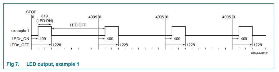
Example 1:(Assume that LED0 is used for output, and (delay time) +(PWM duty cycle) ≤ 100%)
Delay time = 10%; PWM duty cycle = 20%(LED on time = 20%; LED off time = 80%).
Delay time = 10% = 409.6 ≈ 410 counts = 19Ah.
Since the counter ranges from 0 to 4095,1 should be subtracted, therefore the delay time = 199h counts.
LED0_ON_H = 1h; LED0_ON_L = 99h (the LED starts to turn on after the delay count reaches 409) LED on-time = 20% = 819.2 ≈ 819 counts.
LED turn-off time = 4CCh (decimal 410 + 819 - 1 = 1228) LED0_OFF_H = 4h; LED0_OFF_L = CCh (the LED starts to turn off after counting up to 1228)
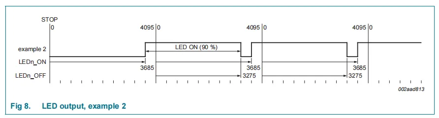
Example 2:(Assume LED4 is used for output, and (delay time) +(PWM duty cycle) > 100%) Delay time = 90%; PWM duty cycle = 90%(LED on time = 90%; LED off time = 10%).
Delay time = 90% = 3686.4 ≈ 3686 counts - 1 = 3685 = E65h. LED4_ON_H = Eh; LED4_ON_L = 65h (the LED will turn on after the delay count reaches 3685)
LED turn-on time = 90% = 3686 counts. Since the sum of the delay time and the LED turn-on period of the duty cycle is greater than 4096 counts, the LEDn_OFF count will appear in the next frame.
Therefore, subtract 4096 from the LEDn_OFF count to get the correct LEDn_OFF count.
LED turn-off time = CCBh (decimal: 3685 + 3686 - 4096 = 3275) LED4_OFF_H = Ch; LED4_OFF_L = CBh (the LED starts to turn off when the count reaches 3275)
2.7.1.5 Control for Turning All LEDs On and Off
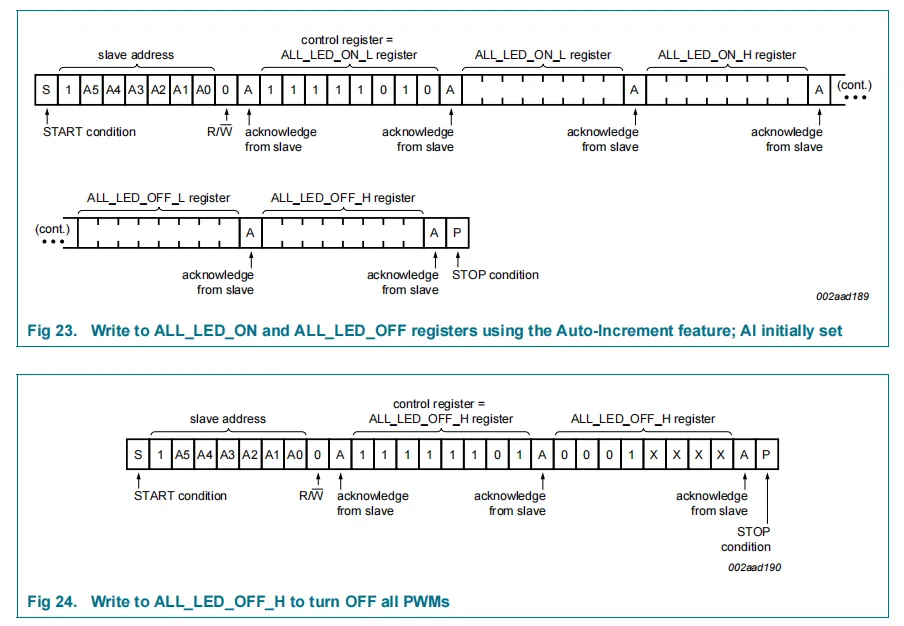
ALL_LED_ON and ALL_LED_OFF registers only require four I²C bus write sequences to fill all the on and off registers with the same pattern.
Table 8: Bit Description Legend for ALL_LED_ON and ALL_LED_OFF Control Registers (Addresses FAh to FEh): * indicates default value
| Address | Register | Bit | Symbol | Access | Value | Description |
| FAh | ALL_LED_ON_L | 7:00 | ALL_LED_ON_L[7:0] | Write-only | 0000 0000* | ON count for all LEDs, 8 most significant bits |
| FBh | ALL_LED_ON_H | 7:05 | Reserved | Read-only | 000* | Not writable |
| 4 | ALL_LED_ON_H[4] | Write-only | 1* | All LEDs fully on | ||
| 3:00 | ALL_LED_ON_H[3:0] | Write-only | 0000* | ON count for all LEDs, 4 most significant bits | ||
| FCh | ALL_LED_OFF_L | 7:00 | ALL_LED_OFF_L[7:0] | Write-only | 0000 0000* | OFF count for all LEDs, 8 most significant bits |
| FDh | ALL_LED_OFF_H | 7:05 | Reserved | Read-only | 000* | Not writable |
| 4 | ALL_LED_OFF_H[4] | Write-only | 1* | All LEDs fully off | ||
| 3:00 | ALL_LED_OFF_H[3:0] | Write-only | 0000* | OFF count for all LEDs, 4 most significant bits | ||
| FEh | PRE_SCALE | 7:00 | PRE_SCALE[7:0] | Read/Write | 0001 1110* | Prescaler for setting the PWM output frequency (default 200 Hz) |
LEDn_ON and LEDn_OFF have a count range from 0 to 4095, and these two count registers must never be programmed to the same value.
Since the loading of the LEDn_ON and LEDn_OFF registers is performed via the I²C bus and is asynchronous to the internal oscillator, these changes must be updated at the end of the low-level period to avoid visual artifacts when modifying the turn-on and turn-off values.
2.7.1.6 PWM Frequency Prescaler (PRE_SCALE)
The minimum value that the hardware-forced PRE_SCALE register can load is "3". This register defines the frequency of output modulation, and the prescaler value is determined by Equation 1:

where update_rate is the required output modulation frequency. For example, for an oscillator with a clock frequency of 25 MHz and a default output frequency of 200 Hz:

If the PRE_SCALE register is set to "0x03h", the maximum PWM frequency is 1526 Hz; if it is set to "0xFFh", the minimum PWM frequency is 24 Hz.
The PRE_SCALE register can only be set when the SLEEP bit of the MODE1 register is set to logic 1.
2.7.1.7 Subaddresses 1 to 3 (SUBADR1 to SUBADR3)
Table 9: Bit Description Legend for SUBADR1 to SUBADR3 – I²C Bus Subaddress Registers 0 to 3 (Addresses 02h to 04h): * indicates default value
| Address | Register | Bit | Symbol | Access | Value | Description |
| 02h | SUBADR1 | 7:01 | A1[7:1] | Read/Write | 1110 001* | I²C-bus subaddress 1 |
| 0 | A1[0] | Read-only | 0* | Reserved | ||
| 03h | SUBADR2 | 7:01 | A2[7:1] | Read/Write | 1110 010* | I²C-bus subaddress 2 |
| 0 | A2[0] | Read-only | 0* | Reserved | ||
| 04h | SUBADR3 | 7:01 | A3[7:1] | Read/Write | 1110 100* | I²C-bus subaddress 3 |
| 0 | A3[0] | Read-only | 0* | Reserved |
Sub-addresses can be programmed via the I²C bus. Their default values upon power-up are E2h, E4h, and E8h, and the device will not acknowledge these addresses after power-up (the corresponding SUBx bits in the MODE1 register are 0).
Once the subaddress is programmed to the correct value, the SUBx bit in the MODE1 register must be set to logic 1 for the device to respond to these addresses.
It only indicates that the 7 most significant bits of the I²C bus sub-address are valid, and the least significant bit of the SUBADRx register is a read-only bit (0).
When the SUBx position is logic 1, the corresponding I²C bus sub-address can be used in an I²C bus read or write sequence.
2.7.1.8 All Call Address Register (ALLCALLADR)
Table 10: Bit Description Legend for ALLCALLADR - LED Global Call I²C Bus Address Register (Address 05h): * indicates default value
| Address | Register | Bit | Symbol | Access | Value | Description |
| 05h | ALLCALLADR | 7:01 | AC[7:1] | Read/Write | 1110 000* | LED All Call I²C-bus address register |
| 0 | AC[0] | Read-only | 0* | Reserved |
The LED global call I²C bus address allows all PCA9685 devices on the bus to be programmed simultaneously (the ALLCALL bit in the MODE1 register must be set to 1, which is the default power-on state). This address can be programmed via the I²C bus, can be used in I²C bus read or write sequences, and can also be programmed as a sub-call address.
This only indicates that the 7 most significant bits of the fully invoked I²C bus address are valid, and the least significant bit of the ALLCALLADR register is a read-only bit (0).
If the ALLCALL bit is 0, the device will not acknowledge the address programmed in the ALLCALLADR register.
2.7.2 Active-Low Output Enable Input
The active-low output enable (OE) pin can enable or disable all LED outputs simultaneously.
- When the OE pin is at a low level, all LED outputs are enabled, and follow the output states defined in the LEDn_ON and LEDn_OFF registers, as well as the polarity defined by the INVRT bit in the MODE2 register.
- When the OE pin is at a high level, all LED outputs are programmed to the value defined by OUTNE[1:0] in the MODE2 register.
Table 11: OE = 1
| OUTNE1 | OUTNE0 | LED output |
| 0 | 0 | 0 |
| 0 | 1 | 1 if OUTDRV = 1, high-impedance if OUTDRV = 0 |
| 1 | 0 | High-impedance |
| 1 | 1 | High-impedance |
The OE pin can be used as a synchronization signal to switch multiple PCA9685 devices simultaneously, which requires an external clock reference that provides the blink period and duty cycle.
The OE pin can also be used as an external dimming control signal. The external clock frequency must be high enough to avoid being visible to the human eye, and the duty cycle determines the LED brightness.
2.7.3 Power-on Reset
When power is applied to V DD, the internal power-on reset keeps the PCA9685 in a reset state until V DD reaches VPOR. At this point, the reset state is released, and the PCA9685 registers and the I²C bus finite-state machine are initialized to their default states. After this, V DD must be dropped below 0.2 V to reset the device.
2.7.4 Software Reset
The Software Reset Call (SWRST Call) allows all devices on the I²C bus to be reset to their power-on state values via an I²C bus command in a specific format. For proper execution, it is necessary to ensure that the I²C bus functions normally and no device is holding the bus suspended.
The definition of the SWRST Call function is as follows:
- The I²C bus master sends a START command.
- The master device sends the reserved SWRST I²C bus address "0000 000", with the R/W bit set to "0"(write).
- The PCA9685 device acknowledges after detecting the general call address "0000 000"(00h). If the R/W bit is set to "1"(read), no acknowledgment will be returned to the master device.
- After the general call address is sent and acknowledged, the master device transmits a 1-byte specific value (SWRST data byte 1): a. Byte 1 = 06h: Only the PCA9685 will acknowledge this value; if byte 1 is not equal to 06h, the PCA9685 will not acknowledge. If more than 1 byte of data is sent, the PCA9685 will no longer acknowledge.
- After the correct byte (SWRST data byte 1) is transmitted and correctly acknowledged, the master device sends a STOP command to terminate the SWRST Call: the PCA9685 will then reset to its default values (power-on values) and can be addressed again within the specified bus free time (tBUF).
The I²C bus master must treat a non-acknowledge from the PCA9685 at any time as an "abort of the SWRST Call". Only when the format of the SWRST Call sequence is incorrect will the PCA9685 not initialize its register reset.
2.7.5 Usage of PCA9685 with and without external drivers
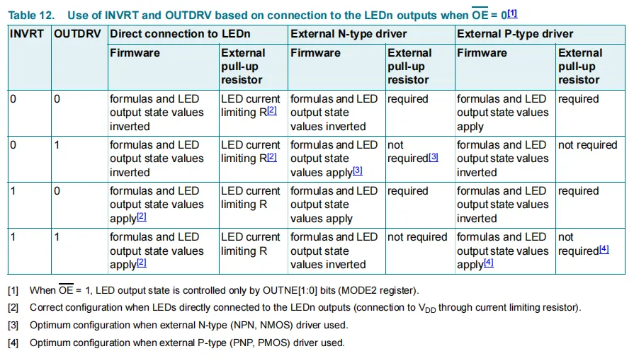
The LED output drivers of the PCA9685 only withstand up to 5.5 V, and can sink a maximum current of 25 mA at 5 V. If the device needs to drive LEDs with higher voltage and/or larger current, an external driver is required.
- The INVRT bit of the MODE2 register allows the LED PWM control firmware to remain unchanged when only the type of external driver is modified. This bit enables inverting/non-inverting control over the LED output polarity when OE= 0.
- The OUTDRV bit in the MODE2 register can reduce the number of external components required to control external drivers (N-type or P-type devices).
2.7.6 I²C Bus
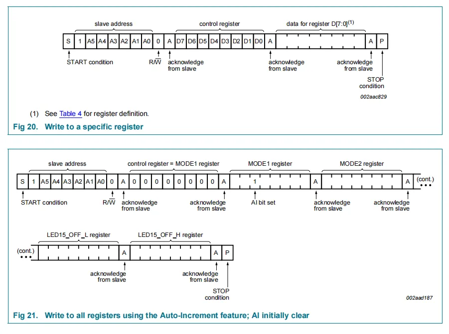
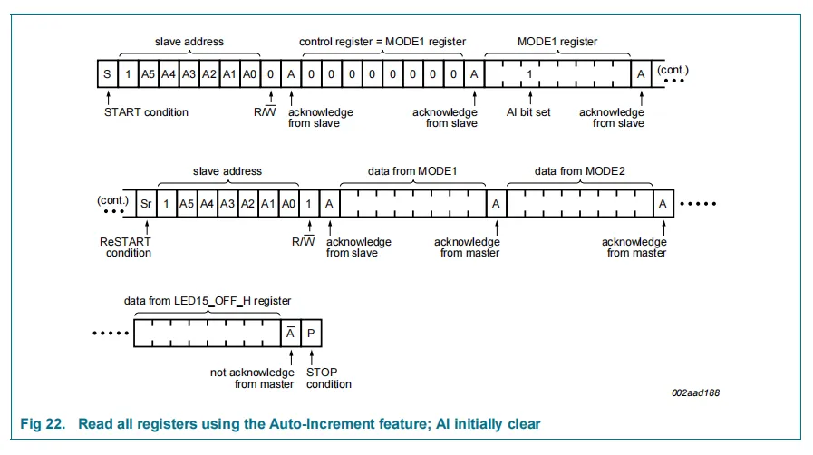
The I²C bus is used for bidirectional two-wire communication between different ICs or modules. The two wires are the Serial Data Line (SDA) and the Serial Clock Line (SCL) respectively. When connected to the output stage of a device, both of these lines must be connected to the positive power supply via pull-up resistors. Data transmission can only be initiated when the bus is idle.
PCA9685PW, 118 The I²C bus slave address is shown in Figure 4. To save power, the hardware selectable address pins do not have internal pull-up resistors integrated, so they must be pulled high or low.
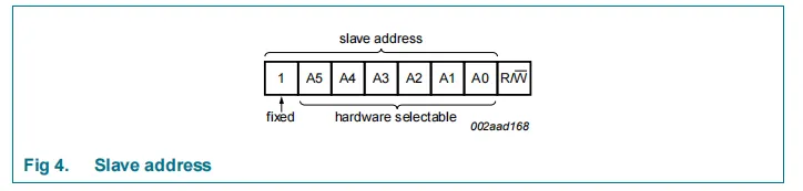
The last bit of the address byte defines the operation to be performed. A logic 1 selects a read operation, and a logic 0 selects a write operation.
2.7.6.1 Bit Transmission
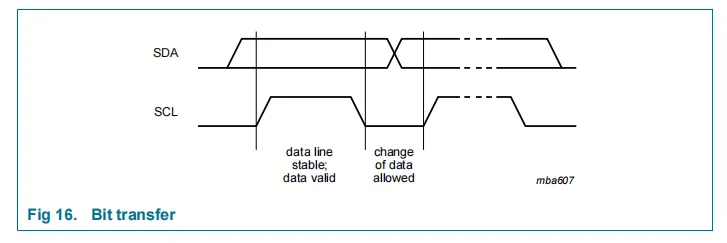
One data bit is transmitted during each clock pulse. The data on the SDA line must remain stable during the high level of the clock pulse, as any change in the data line at this time will be interpreted as a control signal (see Figure 16).
2.7.6.2 Start and Stop Conditions
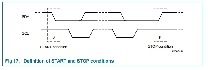
When the bus is idle, both the data line and the clock line remain at a high level. A high-to-low transition of the data line while the clock is high is defined as a start condition (S); a low-to-high transition of the data line while the clock is high is defined as a stop condition (P)(see Figure 17).
2.7.6.3 System Configuration
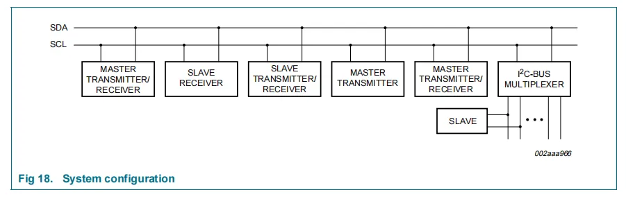
The device that generates messages is the "transmitter", and the device that receives messages is the "receiver". The device that controls messages is the "master device", and the device controlled by the master device is the "slave device"(see Figure 18).
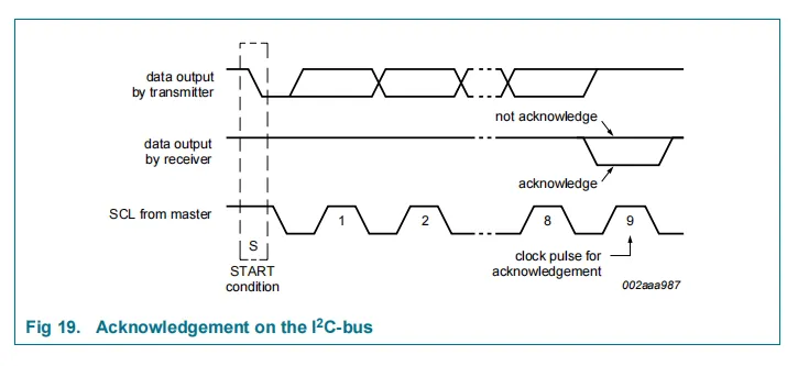
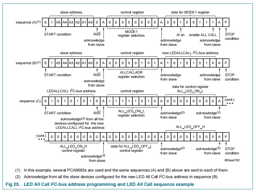
2.7.6.4 Response
Between the start and stop conditions, there is no limit on the number of data bytes transmitted from the transmitter to the receiver. Each 8-bit byte is followed by 1 acknowledge bit. The acknowledge bit is a high level set by the transmitter on the bus, while the master device generates an additional acknowledge-related clock pulse.
The addressed slave receiver must generate an acknowledge after the reception of each byte. The master must also generate an acknowledge after receiving each byte output by the slave transmitter. The acknowledging device must pull the SDA line low during the acknowledge clock pulse, so that the SDA line remains stably low during the HIGH period of the clock pulse associated with the acknowledge; setup time and hold time shall be taken into account.
The master receiver must signal the end of data to the transmitter by not generating an acknowledge for the last byte output by the slave device's clock. At this point, the transmitter must hold the data line high to allow the master to generate a stop condition.
2.8 PCB Routing Precautions
None.
III. Circuit Engineering
3.1 Circuit Source Engineering
To obtain the circuit source project, please follow the official account [Freak Embedded]
3.2 Module Usage Instructions
SCH_Schematic1_I2C Bus Unipolar Stepper Motor Driver Module-V1.0.0_2025-11-18.pdf 2.6 MB
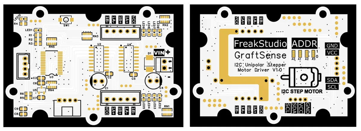
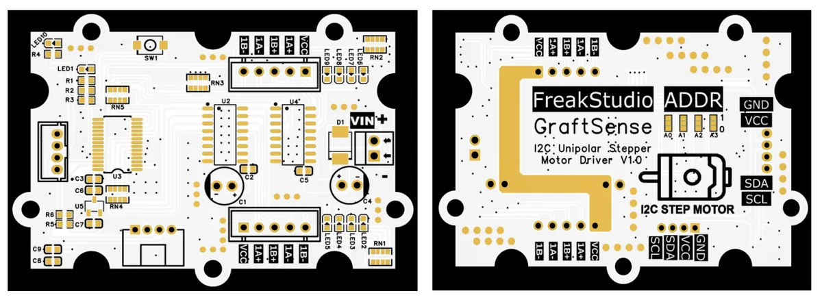
This module uses I2C interface: including SDA (data transmission pin), SCL (clock synchronization pin) core communication pin, and equipped with VCC (power input), GND (signal ground) pin to complete power supply and electrical matching; the module is designed with dual I2C communication interfaces, which can flexibly dock different main control devices and improve connection adaptability.The interface is equipped with ADDR (A0 - A3) address selection pins. By adjusting the level states of these pins, the I2C communication address of the module can be modified, which supports cascading multiple modules on the same I2C bus to meet the requirements of multi-stepper motor cooperative driving scenarios. Meanwhile, it integrates a pull-up resistor circuit, which can ensure the stability of I2C communication without additional external components. This interface is mainly used to transmit control instructions, and cooperates with the PWM generator to realize precise control over operating parameters of the stepper motor such as rotating speed and step angle.
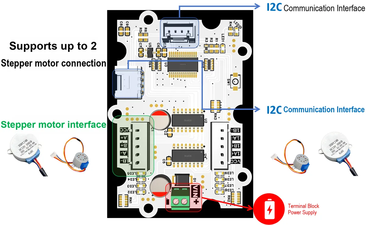
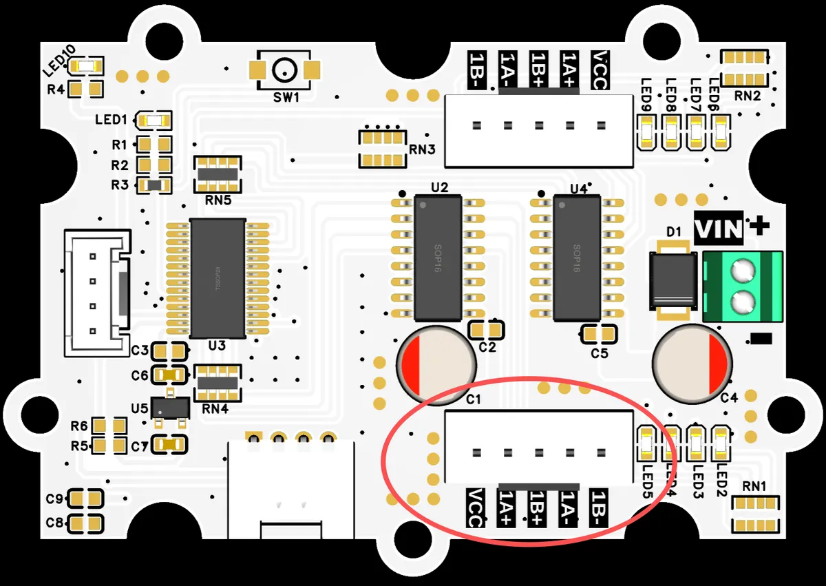
The following are the IIC interfaces led out from the module. The two interfaces only differ in terminals while sharing the same pins, and you can refer to the physical diagram below:
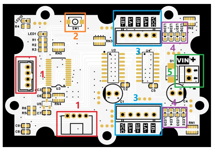
In the physical diagram, the functions of each terminal and button are described as follows:
- No. 1: two
IICinterfaces, which only differ in terminal form but share the same pins. - Item 2: Motor
PWMoutput enable control key: press the key todisable PWMoutput, and release the key to enable it. - Item 3: Two motor output terminals.
- No. 4: When the motor drive port outputs a high level, the corresponding LED indicator will light up.
- Item 5: The
IICinterface power supply of the module is separated from the motor power supply, and the terminal of item 5 is used for external power input of the stepping motor.
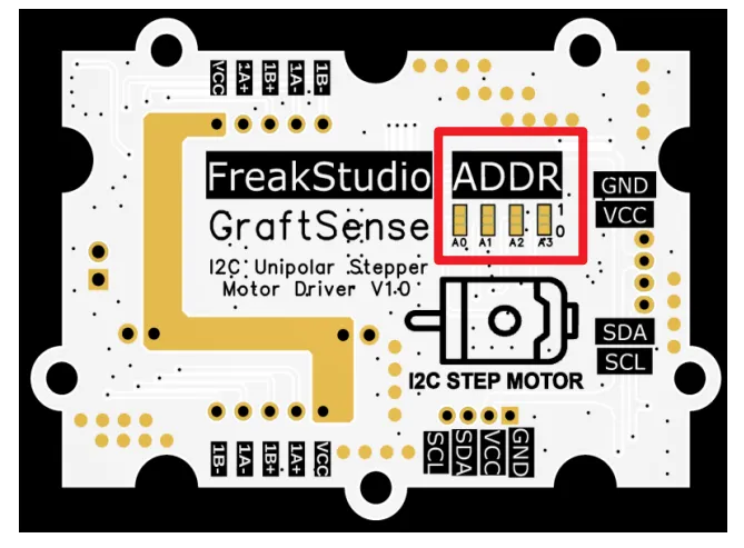
The address selection pins of the module can be selected by soldering the three short-circuit points. For the relevant address description, please refer to Section 2.7.6. The positions of the three short-circuit points on the physical object are as follows:
3.3 Application Experiment
Here, we use the GraftPort-RP2040 development board for testing, and the I2C bus unipolar stepper motor driver module uses the I2C interface to communicate with the main controller.
Here, we first use the HY2.0-4P cable to connect the module to the GraftPort-RP2040 development board's I2C0 interface. Meanwhile, it is also required to use the LM2596S adjustable power supply module to provide 5V external power supply to the I2C bus unipolar stepper motor driver module 's VIN interface, and connect the 28BYJ-48-5V unipolar stepper motor to the No. 1 stepper motor interface:
The overall connection diagram is shown as follows:
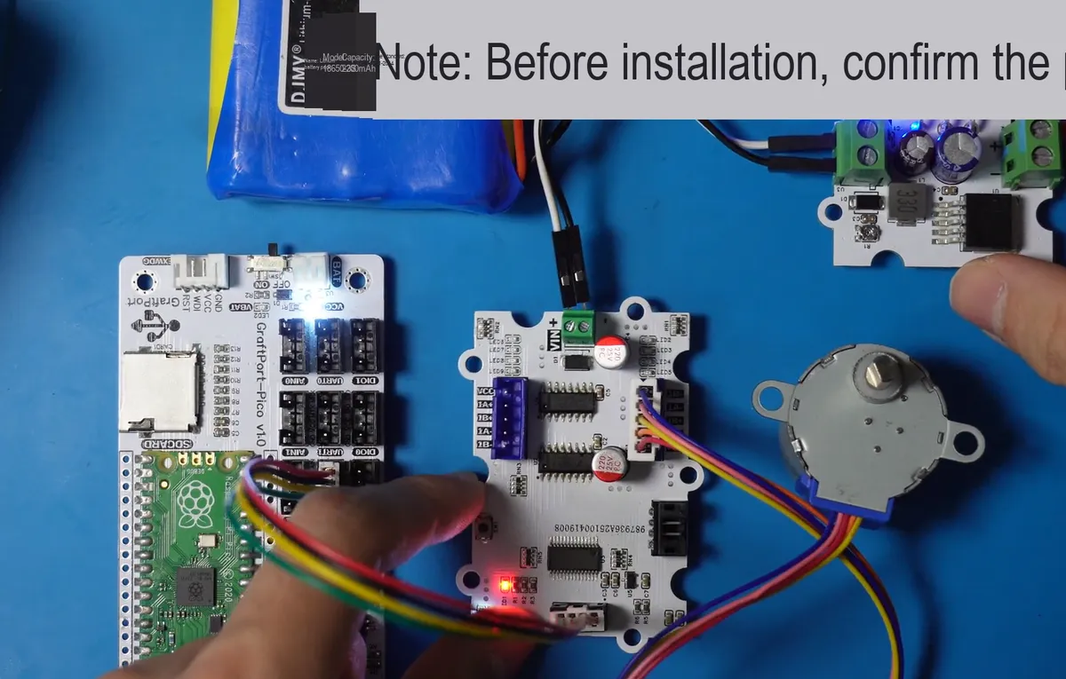
The module connections are shown in the following table:
connection object | development board pins | Module Pins | Description |
Development Boards and Modules | Pin 4 |
| I2C data transmission line, corresponding to |
Development Boards and Modules | Pin 5 |
| I2C clock signal line, corresponding to |
Drive Module and Stepper Motor | - | 5-wire terminal | - |
Power Supply and Modules | - | VIN | LM2596S Adjustable Power Supply Module Power Supply |
Here, we need to search for the relevant driver packages on uPyPI: https://upypi.net/zh/
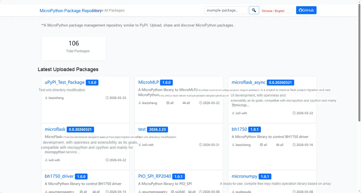
Enter bus_step_motor_driver to search, and the following will be displayed:

Click to copy the local installation command:
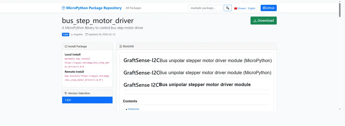
You can download it via the mip tool. Below are the usage commands for the mpremote tool:
mpremote mip install github:FreakStudioCN/GraftSense-Drivers-MicroPython/motor_drivers/bus_step_motor_driverAfter importing the I2C bus unipolar stepper motor driver module - MicroPython driver code, copy the following main.py code into our project:
# Python env   : MicroPython v1.23.0 on Raspberry Pi Pico
# -*- coding: utf-8 -*-
# @Time    : 2025/1/19 AM 10:57
# @Author  : Li Qingshui
# @File    : main.py
# @Description : Bus stepper motor expansion board example program

# ======================================== Import Modules =========================================

# Import hardware-related modules
from machine import Pin, I2C
# Import time-related modules
import time
# Import custom module
from pca9685 import PCA9685
# Import the DC motor control module
from bus_step_motor import BusStepMotor

# ======================================== Global Variables ============================================

# External PWM expansion chip address
PCA9685_ADDR = 0

# ======================================== Functions ============================================

# ======================================== Custom Classes ============================================

# ======================================== Initialization ==========================================

# Power-on delay of 3 s
time.sleep(3)
# Print debug message
print("FreakStudio: Using PCA9685 to control step motor")

# Create a hardware I2C instance using the I2C0 peripheral, with a clock frequency of 400KHz, SDA pin 4, and SCL pin 5
i2c = I2C(id=0, sda=Pin(4), scl=Pin(5), freq=400000)

# Start scanning for devices on the I2C bus and return a list of slave addresses
devices_list = i2c.scan()
print('START I2C SCANNER')

# If devices_list is empty, no device is connected to the I2C bus
if len(devices_list) == 0:
    print("No i2c device !")
# If not empty, print the slave device addresses
else:
    print('i2c devices found:', len(devices_list))
    # Iterate over the slave device address list
    for device in devices_list:
        # Check whether the address is between 0x40 and 0x4F; if so, it is a PCA9685 chip address
        if 0x40 <= device <= 0x4F:
            print("PCA9685 I2C hexadecimal address: ", hex(device))
            PCA9685_ADDR = device

# Create a PCA9685 instance using the I2C0 peripheral
pca9685 = PCA9685(i2c, PCA9685_ADDR)

# Create a stepper motor instance using the PCA9685 instance, with 4 motors
bus_step_motor = BusStepMotor(pca9685, 4)

# ========================================  Main Program  ===========================================

# Enable stepper motor continuous motion mode: motor number 1, forward direction, single-phase drive mode, speed 10
bus_step_motor.start_continuous_motion(1, BusStepMotor.FORWARD, BusStepMotor.DRIVER_MODE_SINGLE, 10)
# Delay 10 s
time.sleep(10)
# Stop stepper motor continuous motion mode
bus_step_motor.stop_continuous_motion(1)

# Enable stepper motor step motion mode: motor number 1, forward direction, single-phase drive mode, speed 10, 10 steps
bus_step_motor.start_step_motion(1, 1, 0, 100, 1000)
To flash the code, open a terminal and use the mpremote tool to connect to the main controller; the output is as follows:
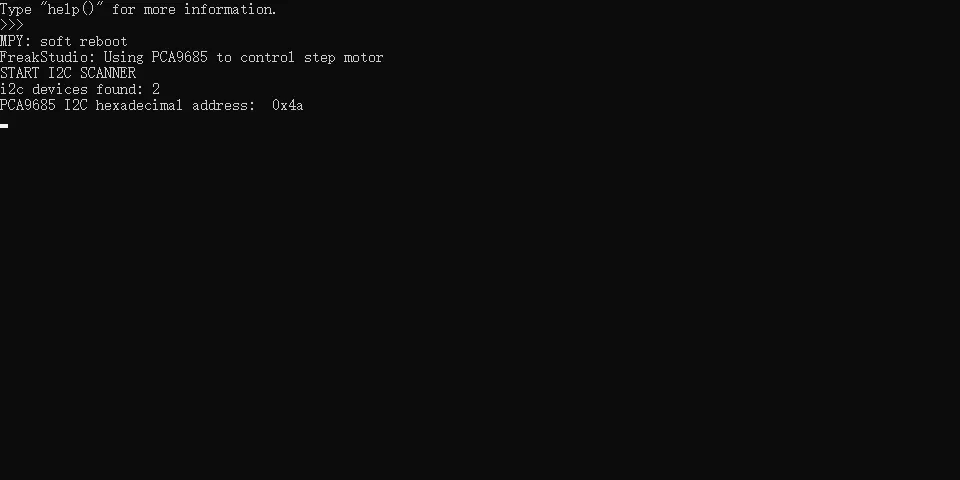
It can be seen that the address of the module is output correctly, and the stepping motor can rotate normally as programmed in the code:
IV. Drivers
bus_step_motor_driver.zip 11 KB
5. BOM & Recommended Alternative Parts
None.
VI. Revision History
Document Version | Revision Date | Modifier | Revised Content |
v1.0 | 2025-11-18 | Xing Gao | Initialize Document |
v1.1 | 2025-12-29 | Li Zisheng | Add production files and application experiments. |
v1.2 | 2025-12-31 | Sin Ruili | Create an open version of the document based on the internal document version v1.1. |
v1.3 | 2026-03-29 | Sin Ruili | Modified the application experiment section |
VII. Relevant Materials
7.1 Chip Datasheet
ULN2003AM_TR Datasheet.pdf 615 KB
PCA9685.pdf 399 KB
7.2 Unique Icons for PCB Silk Screen