The Raspberry Pi Pico is a low-cost, high-performance microcontroller development board officially designed by Raspberry Pi, featuring flexible digital interfaces. In terms of hardware, it adopts the RP2040 microcontroller chip independently developed by Raspberry Pi, is equipped with an ARM Cortex-M0+ dual-core processor, has an operating frequency of up to 133MHz, integrates 264KB of SRAM and 2MB of memory, and also has up to 26 multifunctional GPIO pins on board.In terms of software, you can choose the C/C++ SDK provided by Raspberry Pi or use MicroPython for development. It comes with complete development materials and tutorials, which facilitates quick getting started with development and embedding applications into products.
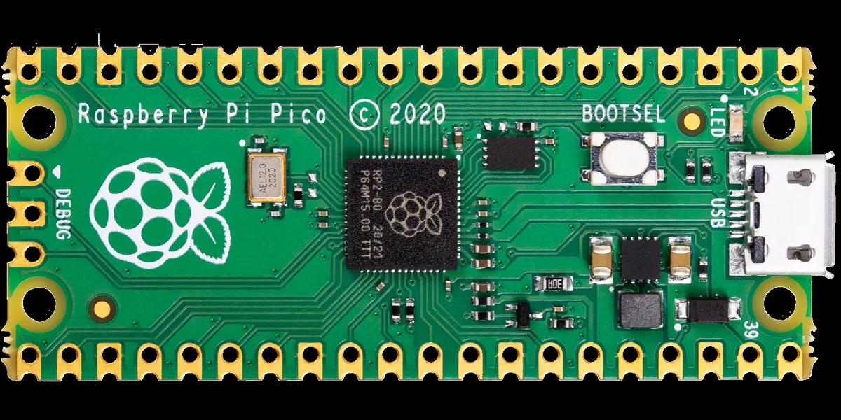
Figure 1.1 Front of the Raspberry Pi Pico Development Board
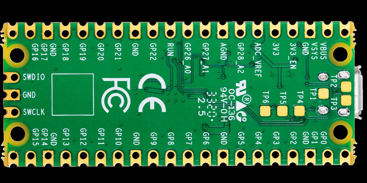
Figure 1.2 Back of the Raspberry Pi Pico Development Board
Differences between a development board and a chip:
What is a "chip"(taking RP2040 as an example): The RP2040 is a single electronic component, an integrated circuit independently developed by Raspberry Pi:
It serves as the core functional carrier of the Pico development board, and itself integrates core computing/storage modules including the ARM Cortex M0+ dual-core processor, 264KB SRAM, and 2MB flash memory;
However, the chip cannot function on its own: it is merely a packaged integrated circuit devoid of peripheral components such as power supply circuits, interfaces, and pin expansion. If you take the RP2040 chip alone, you can neither power it nor connect it to sensors or peripherals.
What is a "development board"(taking the Raspberry Pi Pico as an example): The Raspberry Pi Pico is a finished circuit board based on the RP2040 chip:
It is centered around the RP2040 chip, and integrates necessary peripheral circuits and interfaces at the same time: for example, it comes with an onboard USB power supply circuit, extends the chip's pins into 26 GPIO header pins, and is equipped with a BOOTSEL button, an LED indicator, a USB interface, etc. ;
It is a ready-to-use "finished tool": after developers get the Pico, they don't need to build basic circuits such as power supplies and pin expansions by themselves, and can directly connect it to a computer via USB and plug in sensors to start development.
1.1 Basic Parameters of the Pico Development Board
It adopts the RP2040 microcontroller chip independently designed by the official Raspberry Pi team;
Equipped with a dual-core ARM Cortex M0+ processor, featuring a flexible clock with an operating frequency of up to 133MHz;
It incorporates 264KB of SRAM and 2MB of on-chip Flash, features a stamp-hole design, and can be directly soldered and integrated onto the baseboard independently designed by users.
USB 1.1 host and device support;
Supports low-power sleep and hibernation modes;
It can be recognized as a mass storage device via USB for drag-and-drop program download;
A built-in temperature sensor is integrated on the chip;
On-Chip Accelerated Floating-Point Library
8 programmable I/O (PIO) finite-state machines for custom peripheral support
Flexible user-programmable high-speed IO
It can simulate interfaces such as SD card and VGA
3-pin ARM Serial Wire Debug (SWD) port
A simple yet highly flexible power supply architecture
Can be powered via Micro-USB
Can be powered by an external power source/battery
Plain-language Explanation of MCU Chip Parameters
Adopting the official RP2040 microcontroller chip from Raspberry Pi: it serves as the core computing unit of the development board, integrating all basic functional modules and acting as the "hardware foundation carrier" for the development board to realize computing and control functions.
Dual-core ARM Cortex M0+ processor with an operating frequency up to 133MHz and flexible clocking: is the computing core of the development board:
"Dual-core" means having 2 independent computing units that can process different tasks in parallel (e. g., simultaneously collecting sensor data + controlling peripherals);
The "133MHz clock" serves as the benchmark for computing speed — it can execute 133 million basic instructions per second, which sets the upper limit of task processing speed and meets the efficiency requirements of most lightweight control and Data Acquisition scenarios.
Built-in 264KB SRAM and 2MB on-chip Flash:
SRAM (264KB) serves as the "temporary data buffer" during program operation to store intermediate data generated during program execution, such as real-time values collected by sensors and temporary calculation results. With a capacity of 264KB, it can support scenarios of "simultaneously processing 3 to 5 channels of sensor data plus simple logical operations"; if a task requires processing a large amount of real-time data (e. g., multi-channel high-speed signal acquisition), an SRAM with a larger capacity should be considered.
On-chip Flash (2MB): Yes the "permanent storage area" for programs and fixed data, used to store user-written programs, predefined configuration parameters, etc. (data will not be lost after shutdown). The 2MB capacity can store dozens of lightweight control programs, or programs containing a small number of fixed creatives (such as simple character display data); if a large amount of offline data (such as screen display images) needs to be stored, external peripheral expansion storage is required.
Stamp hole design: it is the hardware integration interface of the development board, which can be directly soldered onto the circuit board independently designed by users to realize the "hardware integration" of the development board into the finished device.
USB 1.1 host and device support → serves as the USB communication interface of the development board and features a "dual-role" design:
As a "device": it communicates with the computer (host computer) to realize program download and data upload;
Act as a "host": connect external USB devices (such as USB flash drives, keyboards) to expand functions like data storage and human-computer interaction.
Supports low-power sleep and hibernation modes → which is the power management mechanism of the development board:
"Sleep Mode": Pauses non-essential modules, retains core data, and supports quick wake-up (applicable to short-term idle scenarios);
"Sleep Mode": Shuts down more hardware modules and retains only basic power supply, featuring lower power consumption (suitable for battery-powered scenarios with prolonged inactivity). This function is an essential support for portable, low-power devices.
Can be recognized as a mass storage device via USB for drag-and-drop program download: Yes A simplified method for program flashing: The development board emulates a "mass storage device" via USB, eliminating the need for dedicated flashing tools. Users only need to copy the program file to this "device" to complete the flashing process, significantly lowering the hardware/operation threshold for entry-level development.
Up to 26 multifunctional GPIO pins (23 digital pins; 3 analog ADC pins): serve as the universal interaction interface between the development board and external devices.
Digital pins: transmit discrete signals of "HIGH/LOW level" to control peripherals (such as LED on/off, motor start/stop) or read signals from digital sensors;
Analog ADC Pins: Convert external continuously varying analog signals (such as the voltage signal from a temperature sensor) into digital values to enable "gradual signal acquisition"(e. g., continuous measurement of temperature and brightness).
2 SPIs, 2 I2Cs, 2 UARTs, 3 12-bit ADCs, and 16 controllable PWM channels → are the dedicated communication/control modules of the development board:
SPI/I2C/UART: are three commonly used "serial communication buses":
SPI: Suitable for high-speed short-distance communication (e. g., connecting displays and high-speed sensors);
I2C: supports multi-device bus sharing (e. g., connecting multiple temperature and humidity sensors simultaneously);
UART: It is a traditional serial communication interface (e. g. for connecting serial port modules, Bluetooth modules);
12-bit ADC: it serves as the quantization unit for analog signals; a 12-bit configuration corresponds to 4096 quantization levels, and more levels lead to higher precision of the collected analog signals (for example, smaller numerical errors when measuring temperature);
16 PWM channels: refer to the "Pulse Width Modulation modules", which adjust the duty cycle of pulses to realize "analog output"(such as continuously regulating motor speed and LED brightness), and multiple channels can simultaneously control different states of multiple devices.
Accurate on-chip clock and timer: as the time reference module of the development board, it provides high-precision time ticks for "timed task triggering"(e. g., periodic sensor data acquisition) and "signal duration measurement"(e. g., pulse signal decoding for infrared remote controls), serving as the core support for all time-related functions.
Built-in temperature sensor on chip: Yes On-chip environment monitoring unit: Capable of real-time monitoring of the chip's own temperature without external sensors, which can be applied to "chip over-temperature protection"(to prevent hardware damage) and "rough ambient temperature detection"(to replace simple external temperature sensors).
On-chip accelerated floating-point library: Yes Floating-point arithmetic optimization module: Improves the efficiency of "numerical calculation with decimals"(e. g., filtering and calibration algorithms for sensor data), avoids the precision loss of ordinary integer arithmetic, and reduces computation time simultaneously.
8 programmable I/O (PIO) finite-state machines for custom peripheral support: are the hardware interface expansion unit of the development board: by programming to define the timing logic of pins, it can simulate non-standard peripheral interfaces (such as SD card read-write interface, VGA display interface), break through the limitations of the chip's native interfaces, and adapt to special peripherals.
3-pin ARM Serial Wire Debug (SWD) port: it is the program debugging interface of the development board: with a dedicated debugging tool, it can read the chip's operating status and set breakpoints for program debugging, which is an essential hardware interface for troubleshooting program errors and optimizing code.
A simple yet highly flexible power architecture — the power management system of the development board: it supports two power supply modes, Micro-USB (for desktop development scenarios) and external power supply/battery (for portable device scenarios), adapts to different usage environments, and improves the scenario compatibility of hardware.
1.2 Pinout Diagram of Pico Development Board
The pinout diagram serves as the "external interface manual" for the Raspberry Pi Pico — when you want to connect external components such as LEDs and sensors to the Pico, randomly connecting pins may either result in incorrect power connection that burns out the hardware, or the selected pins may not support the functions required by the component (for example, if a sensor requires an analog signal but you choose a purely digital pin); referring to the pinout diagram allows you to clearly understand the function of each pin (whether it is a power pin, ground pin, or signal port) and the supported functions, which not only prevents equipment damage due to incorrect connections but also accurately fulfills requirements such as "lighting up an LED" and "enabling a sensor to transmit data".
First, let’s clarify: What exactly is a "pin"? The difference between chip pins and development board pins
What is a pin? A pin can be understood as the "external interface / connecting wire" of a development board — just like the charging port or headphone jack of a mobile phone, it serves as the "channel" that connects the development board to external electronic components (such as sensors and LED lights): it can not only receive power from an external source (power pins), but also transmit control or data signals (signal pins).
Difference between chip pins and development board pins:
Chip pins: These are the tiny metal contacts (small solder points on the chip surface) on the RP2040 chip itself. They are extremely small in size and can only be used after soldering, so ordinary users cannot directly connect wires to them;
Development board pins refer to the interfaces that the Pico forms by expanding the "chip pins" into easily pluggable header pins (i. e., the row of metal pins on the board). Users can directly insert DuPont wires into these pins to connect components such as sensors and motors without soldering by themselves.
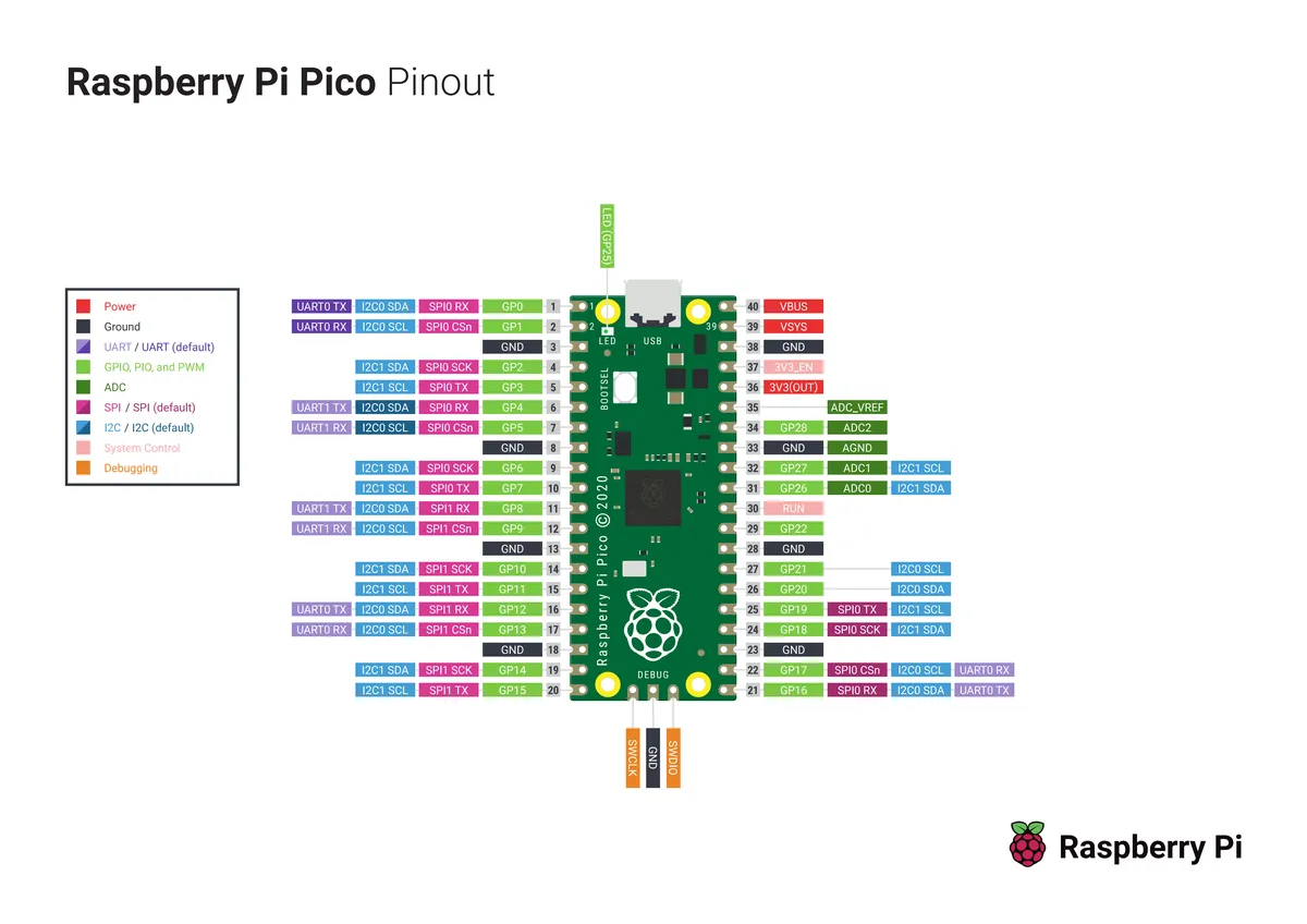
Figure 1.3 Raspberry Pi Pico Development Board Pinout
You can first refer to the "legend" in the top-left corner (colors correspond to pin types: for example, red indicates power pins, and green indicates GPIO pins), then locate the pin numbers on the board (such as GP0 and GP25). The text next to each pin number (such as UART-TX and ADC0) denotes the pin's additional functions. Finally, based on the requirements of the component you are connecting (for instance, if you need 3.3V power supply, look for the red 3V3 pin; if you need analog signal input, look for the pin labeled ADC), match the colors in the legend with the function labels beside the pins, and you will find the appropriate pin.
The definitions of each pin are as follows:
VSYS: 2V~5V power input pin, which serves as the power supply input pin of the development board.
VBUS: It is a 5V power output obtained from the Micro USB interface, which can supply power to electronic components that require a 5V power supply.
3V3 (OUT): 3.3V power supply, which matches the operating voltage of the Pico W. This pin can be used to power external circuits (the maximum output current depends on the RP2040 load and VSYS voltage; it is recommended to keep the load on this pin below 300 mA).
3V3_EN: This pin controls the 3.3V power supply switch. It is set to "ON"(high level) by default. When a low level is input to this pin, the 3V3 (OUT) power output will be turned off, and part of the power supply to the Pico itself will also be controlled accordingly.
RUN: RUN is the enable pin of the RP2040 MCU chip, and you can enable or disable the Pico by applying a high or low level to the RUN pin.
By default, it is at a high level, and there is an internal (on-chip) pull-up resistor connected to 3.3V outside the pin, which has a resistance value of 50kΩ.
Applying a low input level will cause the Pico to stop operating and undergo a reset.
GP0 to GP28: These are general-purpose function interfaces, the most commonly used pins on the Pico, capable of connecting to a wide range of external components: they can either output signals (such as controlling the on/off of an LED) or input signals (such as reading data from sensors). The onboard LED is connected to the GP25 pin.
ADC0 to ADC2: These pins can function either as regular GPIO pins or as "analog input ports" — for example, to measure gradual signals such as temperature levels and light intensity (regular GPIO pins can only detect discrete "on/off" signals).
AGND: AGND (Analog Ground) is specifically used as the reference ground for analog signals such as those on GPIO26 to GPIO29, serving as the "reference ground line" for ADC (Analog-to-Digital Conversion). If you need to measure analog signals with high precision (for example, requiring a very small temperature measurement error), connect this pin to the ground line of external components; if high precision is not required, it can also be directly connected to the common digital ground line (GND).
ADC_VREF: ADC_VREF is the reference voltage pin for improving the accuracy of analog acquisition. By default, it uses the filtered voltage from the Pico's own 3.3V power supply. To achieve higher ADC measurement accuracy, you can connect an external, more stable reference voltage to this pin.
1.3 Pico Development Board Hardware Circuit
Beginners can think of the RP2040 chip as "a phone motherboard without a screen, battery or buttons" — it has core functions, but cannot work without these accessories. These hardware circuits supplement the chip with essential functions such as "power supply, clock, status indicator and interfaces", turning the Pico from a "bare chip" into a "ready-to-use development board".
The Raspberry Pi Pico is equipped with some peripheral circuits of the RP2040 chip, including passive components such as an external Flash memory chip (W25Q16JV), a clock crystal oscillator, and power filter capacitors, as well as a USB connector, a reset button, and an LED indicator. Most of the available pins of the RP2040 chip are routed out on both sides of the Pico development board, and four pins are reserved for internal functions, including driving the onboard LED, powering the development board, and selecting the BOOT mode.
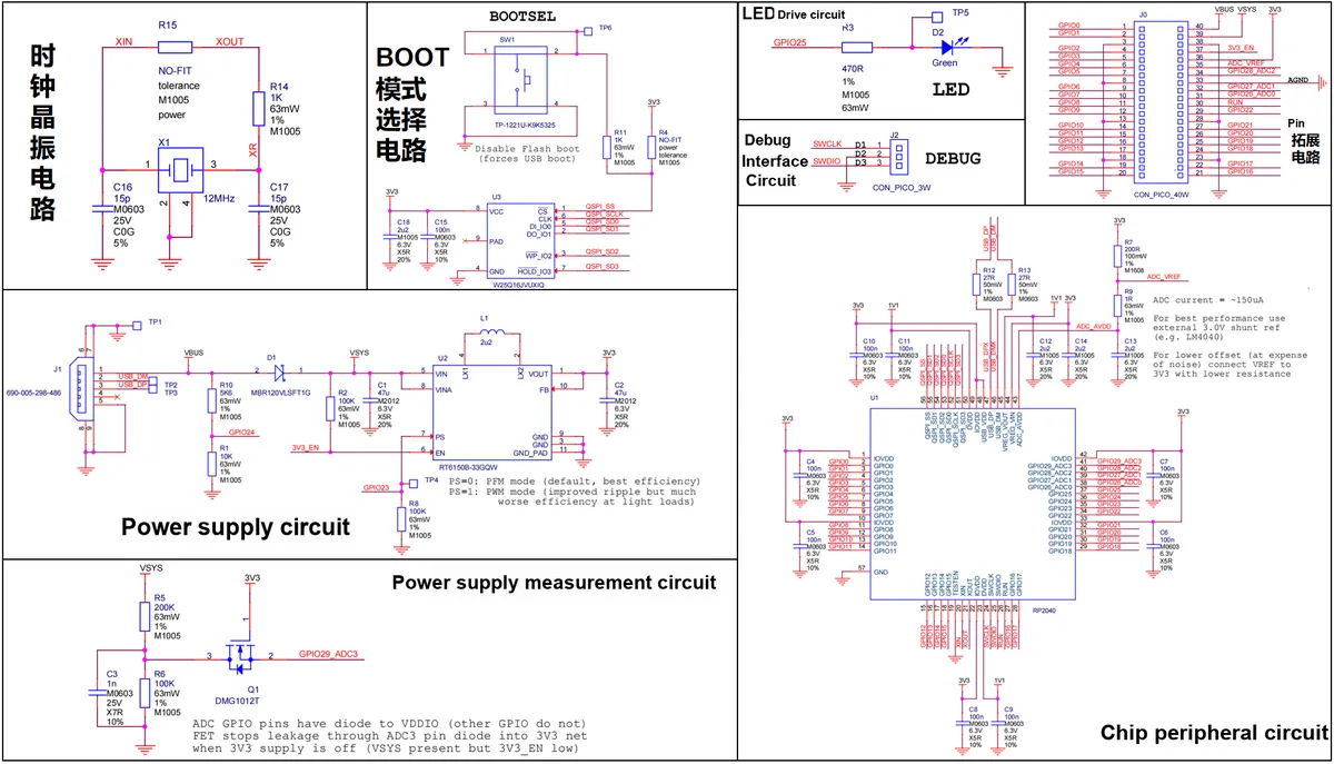
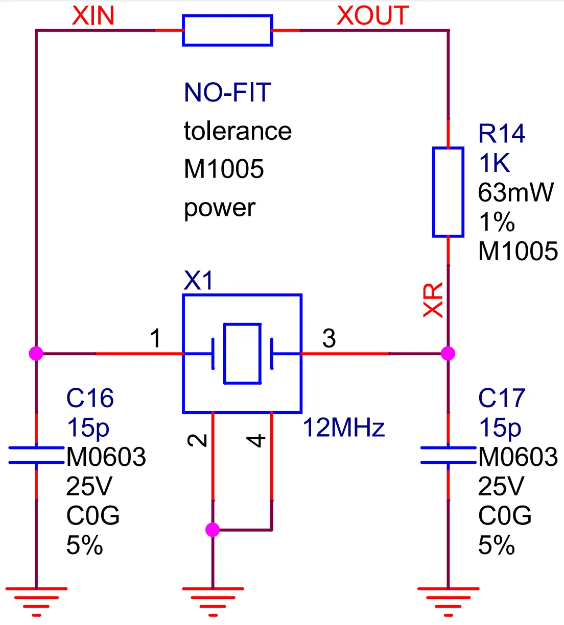
The schematic diagram of the Raspberry Pi Pico is shown below, which consists of an external clock crystal oscillator circuit, a BOOT mode selection circuit, a power supply input circuit, a power supply voltage measurement circuit, an LED indicator driving circuit, a debugging interface circuit, a pin expansion circuit and a chip peripheral circuit, and these will be introduced to you one by one next.
Figure 1.4 Raspberry Pi Pico Development Board Circuit Schematic
Simply put, the peripheral circuits of a Pico development board consist of the following parts:
Clock oscillator circuit: A circuit composed of a 12MHz crystal oscillator (X1 in the diagram) and small components such as capacitors. It acts as the "metronome" for the chip — the chip's operations and communication with peripherals all require precise "timing rhythm", and this circuit provides a stable "beat signal" of 12 million cycles per second to ensure the chip works with accurate timing (for example, timing a 1-millisecond LED flash relies entirely on this beat to calculate time).
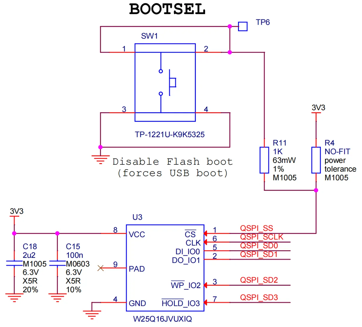
BOOT Mode Selection Circuit: Essentially, it is a small circuit equipped with a BOOTSEL button, serving as the "boot mode toggle switch" for the chip. The chip has two modes during startup:
Normal Mode: Launch the saved program;
BOOT Mode: The firmware flashing state is the "program loading mode" of the Pico: after connecting the Pico to a computer while holding down the BOOTSEL button, the Pico will switch to this state (without launching the old program). At this point, it will be recognized by the computer as a storage device, and you can load new functions onto the Pico by dragging the written program (firmware) into it.
Power supply input circuit: This is the circuit responsible for power management (such as the power management chip U2 in the diagram). We can connect it to a USB (5V) power source or a battery (2-5V); this circuit will stably convert the input voltage to the 3.3V required by the chips, filter out clutter in the voltage, and prevent voltage fluctuations from damaging the chips.
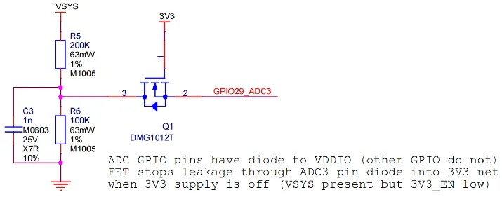
Power Supply Voltage Measurement Circuit: A small circuit that detects the power supply voltage. It acts as the "built-in voltmeter" of the board, capable of measuring the current input power supply voltage in real time (for example, when powered by a battery, it lets you know if the battery is running low), making it convenient for you to monitor the power supply status.
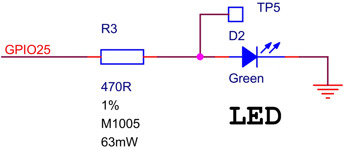
LED Indicator Driver Circuit: A compact circuit for controlling the onboard LED. The chip can toggle this LED on/off via the GPIO25 pin to indicate system status — for example, it flashes when the program is running, and stays steadily lit when power is connected.
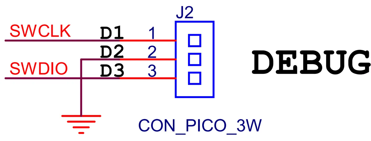
Debug Interface Circuit: This refers to the DEBUG header (a 3-pin header) shown in the diagram, which acts as the "fault diagnosis port" of the board. If your program malfunctions and causes the board to stop working, you can connect a debugging tool to this interface to check the internal operating status of the chip and pinpoint where the program has gone wrong.
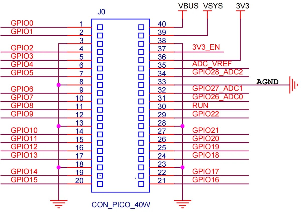
Pin Expansion Circuit: A circuit that converts the chip's pins into header pins (labeled CON_PICO_40W in the diagram). The RP2040 chip itself has very small pins that cannot accept direct wire connections; this circuit expands the chip's pins into standard header pins, allowing you to directly insert DuPont wires into these headers to connect external components such as sensors and motors.
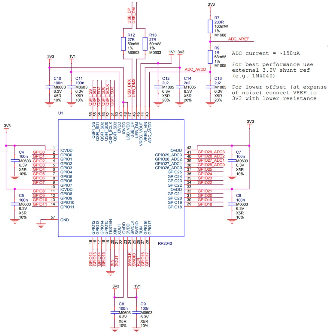
Chip peripheral circuit: A circuit composed of small components such as filter capacitors and resistors around the chip. For example, filter capacitors can filter out clutter in the power supply to make the power supply for the chip more stable; resistors can protect pins from being burned out by excessive current, and prevent the chip from malfunctioning due to external interference or current fluctuations.
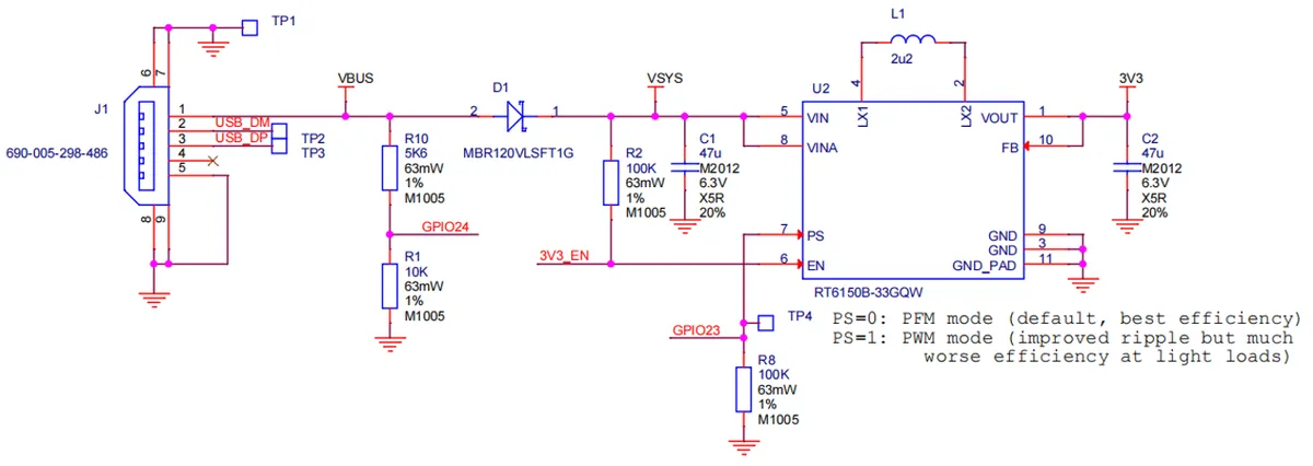
1.3.1 Power Supply Circuit
Figure 1.5 Power Supply Circuit Schematic
The Raspberry Pi Pico can be powered by an external power supply or a Micro-USB cable, and there are two power lines worth our attention:
VBUS line: This is the power supply from the microUSB bus, with a voltage of 5V. If the Raspberry Pi Pico is not powered via the microUSB connector, there will be no power input at this point.
VSYS Line: This is the power supply input line of the DC-DC power chip, with a voltage input range of 1.8~5.5V. The onboard RT6150B can convert the input power into + 3.3V voltage and output it to the MCU chip.
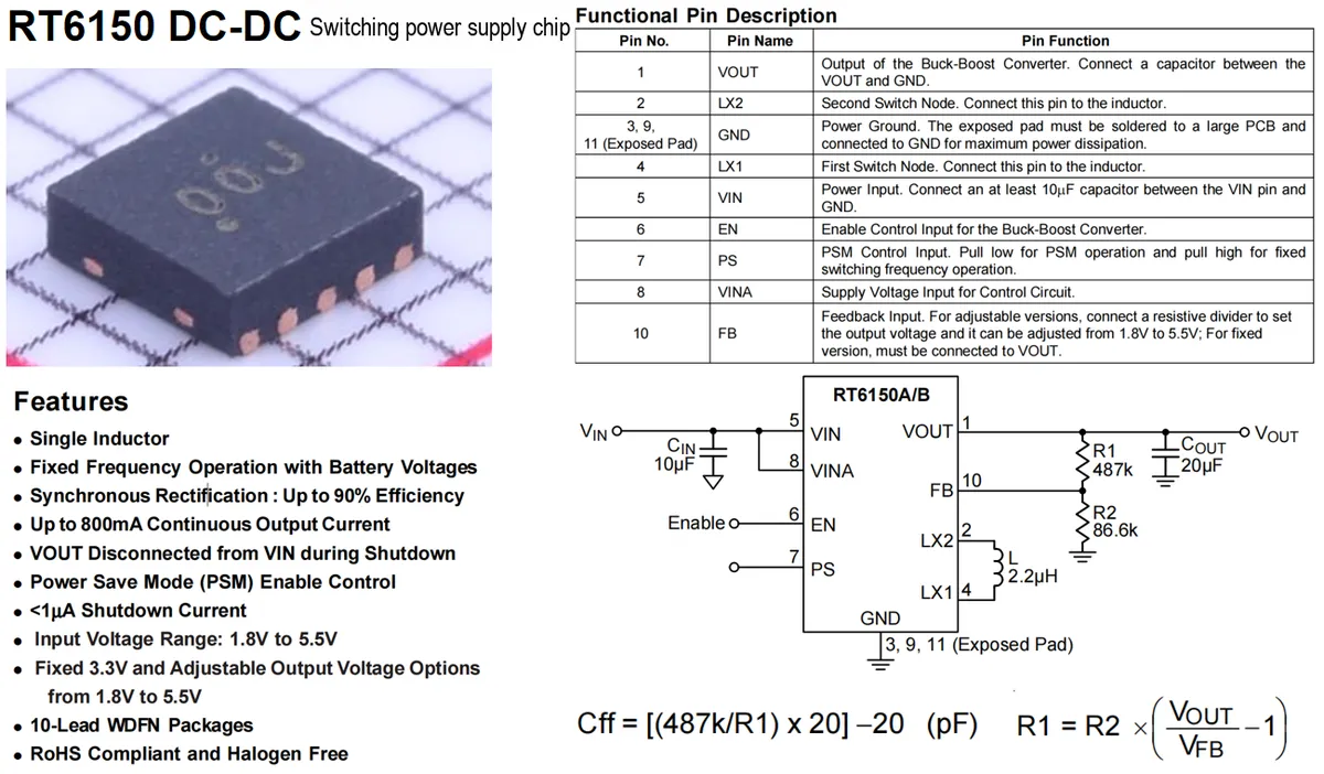
The entire power voltage conversion is implemented by the RT6150B DC-DC power supply chip. The RT6150A/B is a high-efficiency, fixed-frequency switching power converter that operates with input voltages higher than, lower than, or equal to the output voltage. This chip features low static power consumption (the switching operating frequency is set to 1MHz, and the static current in power-saving mode is only 60μA), compact size, selectable operating modes (power-saving mode PSM enable control) and other advantages, and is commonly used in power supply modules for portable products and handheld instruments and meters.
Introduction to RT6150 Power Management IC
(1) Chip Parameters and Reference Circuit Design
Figure 1.6 RT6150 Power Chip Parameters and Reference Circuit Design
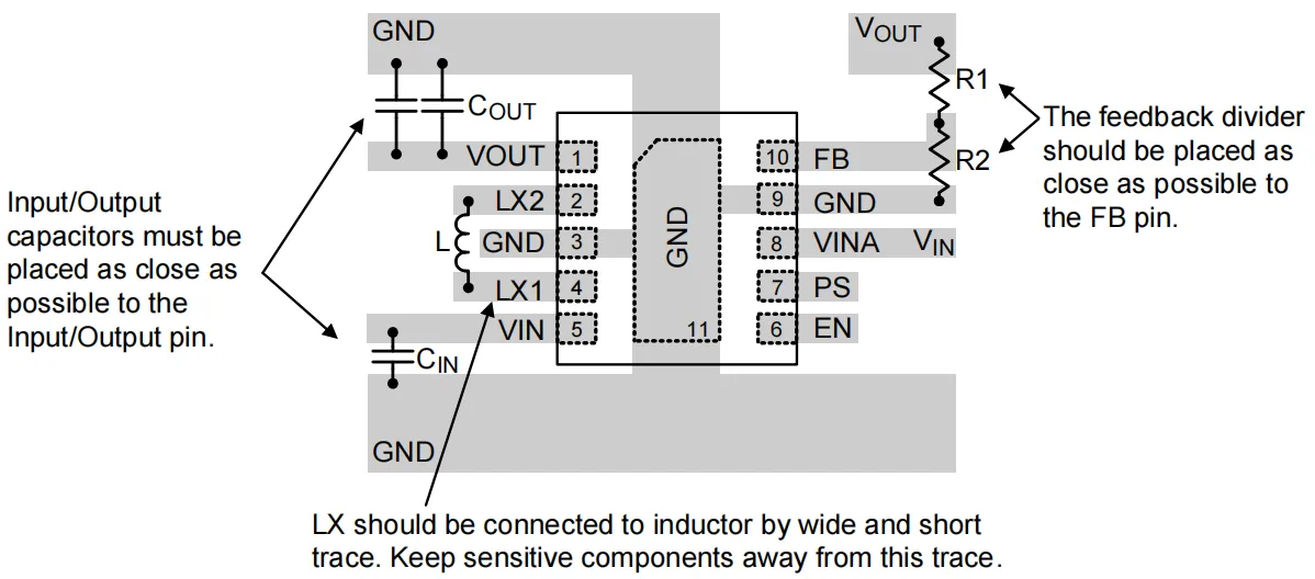
(2) PCB Routing Reference Diagram
Figure 1.7 RT6150 Power Chip PCB Layout Reference
Here, the GPIO23 pin of the Raspberry Pi Pico is connected to the PS pin of the power supply chip, and the operation mode of the power supply chip can be switched by controlling the high and low level output of GPIO23:
PS= 0: PFM (Pulse Frequency Modulation) mode, the default value, which delivers the optimal operating efficiency of the chip. It is the "high-efficiency power-saving mode" that offers the highest efficiency when the power chip is running, and this mode is sufficient for daily use;
PS= 1: PWM pulse width modulation mode, which is the "stable wave heavy load mode", delivers smoother power output and can drive heavier equipment; enabling this mode when using ADC (Analog-to-Digital Conversion) will yield more accurate data.
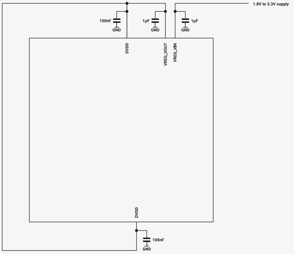
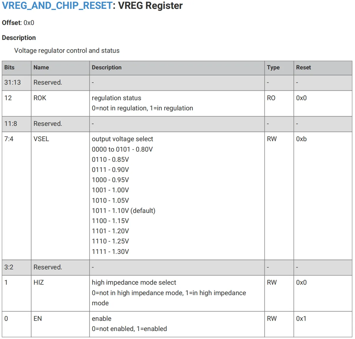
The RP2040 chip on the Raspberry Pi Pico requires two voltage supplies: 3.3V (for I/O) and 1.1V (for the digital core voltage of the chip). Since the RP2040 has an integrated 3.3V-to-1.1V LDO, there is no need to worry about the 1.1V power supply issue.
1.3.2 Clock Crystal Oscillator Circuit
Figure 1.8 Clock Crystal Oscillator Circuit
Chips cannot function without precise "timing rhythm" — for example, tasks like flashing an LED at 1-second intervals or transmitting data in sync with a sensor all rely on a stable "clock signal". This circuit serves as Pico's "external precision metronome", dedicated to providing a stable time reference for the RP2040. Below are its core components and their functions:
Here, a crystal oscillator with SMD3225-4P package and 12MHz frequency is selected. The 15pF capacitors on both sides of the crystal oscillator function to ensure more stable oscillation frequency, and a 1kΩ resistor connected in series in XOUT is used for current limiting, which can prevent the crystal oscillator from reduced service life or damage caused by over-driving. If other different crystal oscillators are selected, these values may need to be adjusted.
When strict timing requirements are not required, the clock of the RP2040 can be selected to be input from the internal oscillator.
1.3.3 BOOT Mode Selection Circuit
Figure 1.9 BOOT Mode Selection Circuit
This circuit incorporates two key functional modules of the Pico: one is the BOOT mode selection circuit that controls the "startup state", and the other is the Flash memory circuit that stores programs. The former helps you switch between the states of "running the stored program" and "loading a new program", while the latter acts as the "built-in small hard drive" for the Pico to store programs. Their specific functions are detailed as follows:
The onboard 2MB QSPI flash memory can be (re-) programmed via the serial wire debug port or through a special USB mass storage device mode.
The upper part is the BOOT mode selection circuit. The startup mode switching button is connected in series with a 1kΩ resistor to the QSPI_SS pin of the RP2040. This series resistor ensures that the content of the Flash runs when the reset button is pressed in BootLoader mode.
When the RP2040 is powered on, the QSPI_SS pin automatically defaults to pull-up, and the RP2040 checks the value of this I/O during the boot process; when QSPI_SS is at logic 0, the RP2040 enters the BootLoader mode of the boot loader driver.
When the BOOTSEL button is not pressed, during reset or power-up: the device enters normal mode, and the MCU boots the pre-stored program from Flash.
When the BOOTSEL button is pressed during reset or power-up, the MCU enters the "new program loading" BootLoader mode, at which point the Pico will appear as a "USB flash drive" on the computer; simply drag and drop a uf2 format program file to update the firmware.
There is a short period during power-up when the state of the QSPI_SS pin cannot be guaranteed, and this can be ensured by adding a pull-up resistor. For the W25Q128 Flash memory, an external pull-up resistor is unnecessary, so it is marked as NO-FIT and can be omitted during soldering.
Below is the Flash memory circuit, whose power supply operates at the same voltage as the 3.3V power pin of the chip. The pins of the W25Q128 are connected to the QSPIx pins of the RP2040. Place 2.2uF and 100nF filter capacitors near the power supply pin (VCC) of the W25Q128 Flash memory to provide a stable 3.3V power supply for the W25Q128JVSIQ.
The steps to flash firmware in USB mode are as follows:
First, turn off the power supply of the circuit board.
Hold down the start button while the circuit board is powered on (i. e., hold down the BOOTSEL button and then connect the USB)
Pico will appear as a USB mass storage device, and you can complete the Flash writing by dragging a special '. uf2' file to the disk
Unplug the USB connector of the Pico and then reconnect it
1.3.4 Power Supply Measurement Circuit
Figure 1.10 Power Supply Measurement Circuit
This circuit is the 'power supply voltage monitoring module' of Pico, which utilizes the ADC (analog signal acquisition) function of the chip to measure the supply voltage of Pico in real time (for example, checking the remaining power of the battery). First, understand the basics of the ADC of the RP2040, then look at the function of this circuit:
The ADC of the RP2040 is a "tool for measuring gradual change signals"(such as measuring voltage levels), and it has 5 acquisition channels:
The four channels correspond to the four pins GPIO26 to GPIO29;
One is the built-in "temperature sensor" inside the chip, which can measure the chip temperature without any external components;
There is also an ADC_VREF pin, which serves as the "reference standard" for ADC voltage measurement (3.3V by default, and it determines the voltage range that the ADC can measure).
These ADC pins are internally protected by reverse diodes and feature a 12-bit resolution (equivalent to dividing the 0~3.3V range into 4096 small steps for more accurate voltage measurement).
The so-called power supply measurement circuit is to use GPIO29 (corresponding to ADC3 channel) to measure the supply voltage (VSYS) of the Pico:
C3 capacitor: filters the voltage signal to make the voltage to be measured more stable and prevent clutter from interfering with the measurement results;
R5 and R6 resistors: Divide the VSYS voltage (max. 5.5V) into 1/3 (since the ADC can only measure up to 3.3V, the divided voltage falls within the measurable range);
Q1 component: Prevents voltage from leaking from the ADC pin into the power supply circuit after the Pico is powered off, serving a protective function;
Finally, GPIO29 will sample the "divided VSYS voltage", and the current supply voltage can be obtained after conversion (for example, when powered by a battery, the battery level can be monitored).
1.3.5 Peripheral Circuit of the Chip
Figure 1.11 Chip Peripheral Circuit
The RP2040 chip serves as the "core brain" of the Pico, but it requires "supporting safeguards" to operate independently — the peripheral circuitry below acts as an "auxiliary module" that complements the chip with essential capabilities such as "communication, power supply, and anti-interference", enabling the chip to work stably and implement functions including USB connection and ADC acquisition, which are specifically divided into the following parts:
USB Communication Section: The two signal pins of the USB interface (USB_DP / USB_DM) must be connected to the USB interface in series with 27Ω resistors — these resistors function as "protection + optimizers": they not only prevent component burnout caused by excessive current in case of a short circuit, but also enable smoother signal transmission and reduce interference, allowing the USB to be used both for firmware programming and for connecting external USB devices.
Chip Power Supply - Internal LDO Power Input: Inside the chip, there is a "voltage converter" that steps down 3.3V to 1.1V to power the core circuitry. The 2.2µF capacitors adjacent to its input and output pins act as voltage stabilizers, filtering voltage fluctuations to ensure a stable 1.1V power supply and prevent the chip from malfunctioning due to unstable voltage.
GPIO Peripheral Power Supply Input: The 100nF small capacitor next to the GPIO pin acts as an "anti-interference filter" that filters out clutter in the power supply, making the GPIO pin more stable when supplying power to or transmitting signals to external components.
TESTEN: This is a pin for factory testing, directly connected to the ground line, and users do not need to handle it.
ADC Reference Power Supply: By default, the ADC uses the Pico's built-in 3.3V as the "reference scale" for voltage measurement; for higher acquisition accuracy, a dedicated external voltage reference chip (e. g., LM4040) can be connected, but in this case the ADC will only be able to measure voltages in the range of 0 to 3.0V.
ADC Power Supply - ADC_AVDD Pin: Supplies 3.3V power to the ADC module, using the stable 3.3V output from the preceding power management chip.
1.3.6 LED Driver Circuit
Figure 1.12 LED Drive Circuit
It is used to test the GPIO25 pin of the RP2040, and its on-off can be controlled via a program.
1.3.7 Debug Interface Circuit
Figure 1.13 Debug Interface Circuit
This circuit serves as Pico's "program debugging port" — when the program you wrote malfunctions (e. g. the board is unresponsive or functions incorrectly), it can help you troubleshoot issues and load code directly, offering more flexibility than regular USB programming. Its specific functions are detailed below:
There are two ways to reprogram the Flash on Pico:
Normal method: Drag and drop the uf2 file via USB (simple but with limited functions);
This SWD debug port (DEBUG interface): It allows you to reset the system, load and run code without pressing any buttons, and also supports "interactive debugging" — meaning you can view the internal operating status of the chip while the program is running, to pinpoint exactly where the program goes wrong.
Additionally:
The SWDIO and SWCLK debug pins of the RP2040 chip have built-in 60kΩ pull-up resistors internally, so no additional resistors are required.
However, the more commonly used term in daily practice is "USB serial port debugging", which represents the most straightforward program download/debug method, and the USB approach is sufficient for most beginners.
1.3.8 Pin Expansion Circuit
Figure 1.14 Pin Expansion Circuit
The pins here are led out through 2 sets of "1×20Pin" stamp holes (each set has 20 pin holes), and the spacing between adjacent holes is 2.54mm — this is a common standard spacing for electronic components, compatible with regular DuPont wires and expansion boards.
The advantage of this design is its "dual-purpose" functionality: it can either be directly connected to components like sensors and LEDs via Dupont wires for experiments, or the Pico can be soldered onto a custom-designed circuit board, making it easy to integrate the Pico into your finished projects (such as small robots or environmental monitoring devices).
1.3.9 Introduction to Test Points
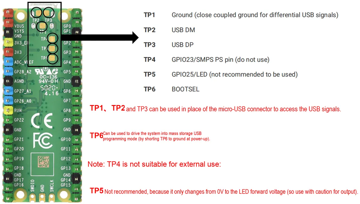
There are 6 test points (TP1 to TP6) accessible on the Raspberry Pi Pico:
Figure 1.15 Raspberry Pi Pico Test Points (TP1~TP6) Function Description
These 'test points (TP1~TP6)' are the 'spare small connectors' reserved on the Pico board — the main interfaces such as Micro-USB and pins are sufficient for regular use, but when you need to batch test whether the development boards are functional, the main interfaces are damaged, or special operations are required, these test points can temporarily replace some functions. The functions of each test point are as follows:
TP1, TP2, TP3: These are "spare USB ports" — if the Micro-USB port on the board is damaged, you can use these three test points to connect USB signals to replace the function of the original USB port;
TP4: Not suitable for external use; ignore it.
TP5: Corresponds to GPIO25 (the pin of the onboard LED), but it is not recommended for use — since its voltage can only vary between 0V and the LED turn-on voltage, which has an excessively narrow range, using it as an output is prone to issues;
TP6: This is the "trigger point for the alternate BOOT mode". If the BOOTSEL button malfunctions, simply short TP6 to the ground line when powering on the device, and it will force the Pico to enter the drag-and-drop programming mode for firmware flashing.
2. Introduction to the RP2040 Chip
RP2040 is the first microcontroller chip launched by Raspberry Pi, featuring the advantages of low power consumption, high performance and low cost.
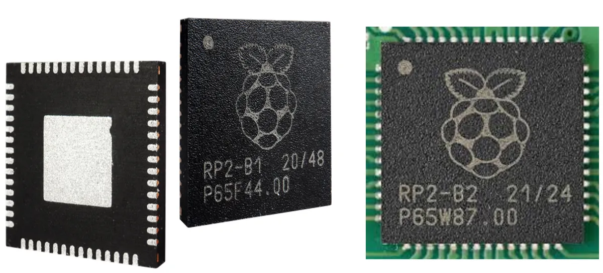
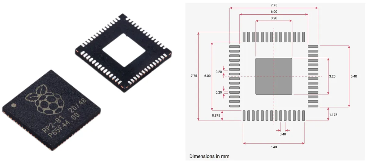
The RP2040 chip is manufactured using a 40nm process, which means the chip is compact in size and low in power consumption, and it comes in a 7×7mm QFN-56 package —that is, the chip is a 7mm square die with 56 small pins, making it easy to solder onto circuit boards:
Figure 2.1 RP2040 Chip in QFN-56 Package: Photo and Dimensions
The specific specifications and parameters are as follows:
Dual-core Arm Cortex-M0 + @ 133MHz
The chip has built-in 264KB SRAM and 2MB onboard flash memory.
Supports off-chip flash memory up to 16MB via a dedicated QSPI bus
Built-in DMA controller (acts as the chip’s "errand runner" to transfer data, so that the chip can focus on computing without wasting computing power)
30 GPIO pins, 4 of which can be used as analog inputs
4 ADC channels, maximum sampling rate of 0.5 MSa/s, 12-bit precision, and support for external reference voltage input
2 UARTs, 2 SPI controllers and 2 I2C controllers
16 PWM channels
USB 1.1 host and device support
8 Raspberry Pi programmable I/O (PIO) finite-state machines for custom peripheral support
Supports UF2-enabled USB mass storage boot mode for drag-and-drop programming
Supports SWD debugging and downloading
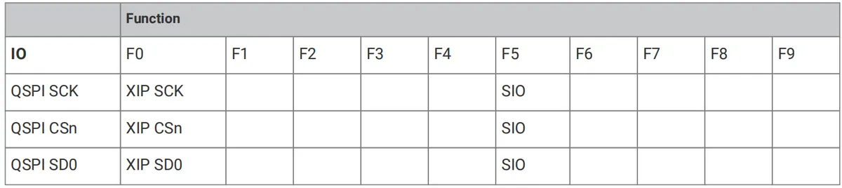
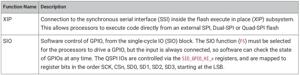
Six dedicated IOs are used for SPI Flash to support XIP (which enables direct reading of programs from external flash without first copying them into the chip)
Built-in temperature sensor
Accelerated floating-point library in ROM
Fully connected AHB crossbar (the "expressway" inside the chip that enables faster data transmission between various components)
Interpolator and integer divider peripherals (more efficient for complex numerical operations such as division and interpolation)
On-chip programmable LDO, used to generate core voltage (it can convert the input voltage into the voltage required by the core by itself, eliminating the need for an additional power supply chip)
2 on-chip PLLs are used to generate USB and core clocks, which produce precise "time beats" to ensure the accurate rhythm of chip operation and USB communication.
What is "encapsulation"?
The core of a chip (the integrated circuit on the silicon wafer) can be understood as a "fragile bare die" — it is thin and delicate, vulnerable to impacts and moisture, and has no directly connectable interfaces, making it impossible to use as-is. "Packaging" is the process of "fitting a protective casing and leading out interfaces" for this bare die:
It serves as the "protective casing" of a chip: it encloses the fragile core circuitry to resist impacts, moisture and dust, thereby preventing damage to the circuits;
It serves as the "external interface" of the chip: metal pins are drawn out from the core circuit to facilitate soldering the chip onto a circuit board, enabling the chip to receive power and transmit signals with external components.
Different packages feature distinct shapes and pin counts; for instance, the "7×7mm QFN-56 package" used for the RP2040: QFN denotes the package type (a flat no-leads form factor), 56 indicates that this package comes with 56 pins, and 7×7mm refers to the dimensional size of the package.
In addition to the QFN package used for the RP2040, these are other common chip packages:
DIP package (Dual In-line Package) Take "DIP-20" as an example: it features long metal pins arranged in two rows, which can be directly inserted into a breadboard or perforated prototype board.
Features: beginner-friendly, easy to insert and solder, and simple to disassemble when damaged; however, it is relatively bulky in size.
Applicable scenarios: Experiments for beginners, prototype verification on breadboards (for example, early 51 single-chip microcontrollers commonly used DIP packages).
SOIC package (Small Outline Integrated Circuit package) For example, "SOIC-16": it is a surface-mount package, with pins being small metal leads on the surface of the circuit board, and its volume is much smaller than that of DIP.
Features: Compact size, suitable for tight circuit board layouts; however, it requires surface-mount soldering, making manual soldering more difficult for beginners compared to DIP packages.
Applicable scenarios: Small consumer electronics (such as chips for Bluetooth modules and small sensors).
QFP package (Quad Flat Package) For example, "QFP-44": its leads are arranged on all four sides of the chip, and it features a higher pin count than SOIC.
Features: It can support more functions (more pins correspond to more chip functions), with a size smaller than DIP but larger than BGA.
Applicable scenarios: Devices with moderate complexity (such as some feature-rich microcontrollers and small industrial control board chips).
BGA package (Ball Grid Array package) Take "BGA-100" for example: its pins are the solder balls on the bottom of the chip (rather than exposed pins), featuring an extremely compact size and a very large number of pins.
Features: It can accommodate a large number of pins (supporting high-performance chips) and has an extremely small form factor; however, it requires professional equipment for soldering and is hardly usable for beginners.
Application scenarios: High-end small devices (e. g., processors in mobile phones and tablets, high-performance sensor chips).
The core differences between these packages lie in their size, pin configuration, and soldering difficulty: DIP (easy to handle) is commonly used by beginners for experiments, SOIC/QFN is typical for compact end products, while BGA is adopted for high-end miniature devices.
USB Flashing Format (UF2) File
UF2 is a brand-new firmware update file format developed by Microsoft for PXT (also known as Microsoft MakeCode), which is particularly suitable for the firmware upgrade process of microcontrollers and embedded devices via Flash memory.
The core features of the UF2 file lie in its divisibility and easy identifiability. Each UF2 file consists of a series of fixed-size (usually 512-byte) data blocks, which can be read independently by the device. When the device detects consecutive data blocks, it will automatically combine them into a firmware image. This design allows the device to start running the update after receiving part of the file, thus improving the reliability of the update.
In addition, UF2 files have a specific trailing structure to facilitate devices in identifying their file type. This feature enables UF2 files to operate seamlessly across various operating systems such as Windows, Linux or macOS, and be compatible with a wide range of development boards.
It has the following characteristics:
Easy to use - Users can upload UF2 files to compatible hardware devices via simple drag-and-drop operations;
Cross-platform compatibility - Works with multiple operating systems and is widely used in various microcontrollers and development boards;
Robustness - Ensures successful firmware updates even in unstable network environments;
Flexibility - Can be easily adapted to different hardware architectures and memory layouts.
XIP —— eXecute In Place
The memory units in a microcontroller can be roughly divided into two categories:
RAM: Variables that need to be rewritten during program execution are all stored in RAM;
ROM: Mainly used to store instruction codes and certain fixed values that cannot be modified after the program runs. For example, all code in. c and. h files, global variables, local variables, constant data defined by the 'const' qualifier, and the code in the startup.asm file are all stored in ROM.
Flash memory, also known as flash, combines the advantages of both ROM and RAM: it not only features the electrically erasable programmable (EEPROM) performance, but also retains data without power supply while enabling fast data readout. In the past, embedded systems consistently used ROM (EPROM) as their storage device; however, in recent years, Flash has fully replaced ROM's position in embedded systems.
During the code execution of a microcontroller unit (MCU), it is usually necessary to read the code from ROM or external flash into a RAM buffer before executing it sequentially. However, many modern NOR QSPI flash memories support the XIP (eXecute In Place) function, under which mode the embedded MCU chip can directly fetch instructions from the NOR QSPI flash for the subsequent decoder and executor to use, without the need to read the code into RAM in advance.Simply put, XIP is a mechanism that enables code to be executed directly in flash memory without being loaded into RAM for execution, which reduces the time required for the kernel to be copied from flash memory to RAM.
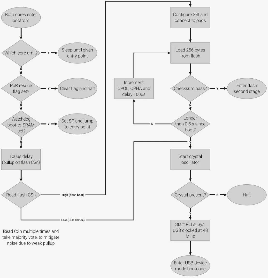
When flashing a self-developed application to the Raspberry Pi Pico, the program is first written to the external Flash, and then when the chip starts up, the bootloader in its internal ROM loads and executes the program via XIP/Cache.
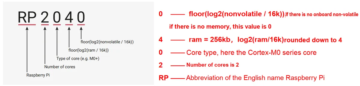
The specific meaning of each symbol in its name RP2040 is as follows:
Figure 2.2 RP2040 Chip Part Number Naming Convention
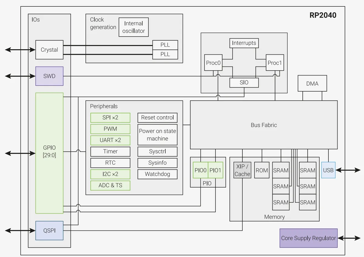
2.1 Block Diagram of the Chip System
For any chip, the block diagram serves as the core starting point for learning — it acts as the chip's "architecture specification" that helps you build a systematic understanding (rather than a scattered list of functions), which is the universal approach to learning all chips. Through the block diagram, you can first grasp the information from the following general dimensions before diving into specific functions:
Clarify the composition of core functional modules: Whether it is a microcontroller, processor or dedicated chip, the block diagram will clearly divide the arithmetic core (such as the dual cores of RP2040), storage units (such as SRAM), peripheral interfaces (such as SPI/I2C), and auxiliary modules (such as clock/power supply), allowing you to quickly understand "what basic components the chip contains" — this is the "component list" for subsequent learning.
Master the architectural logic between modules: The block diagram presents the hierarchical relationship of each module (e. g., the core is the core control layer, and the peripherals are the external interaction layer) and the communication link (e. g., the bus is the interconnection hub between modules), helping you understand "how the components of a chip work together" — for example, the core of all chips accesses memory and controls peripherals through the bus, which is the general logic of chip operation (corresponding to the Bus Fabric interconnection of RP2040).
Clarify the allocation boundaries of hardware resources: Key resources of the chip (such as the number of GPIOs, memory size, and peripheral types) can be directly obtained through the block diagram, which is the premise for subsequent hardware design and program development — for example, by knowing how many UARTs a chip has, it is possible to determine how many serial port devices it can connect simultaneously (corresponding to the 2 UARTs and 30 GPIOs of the RP2040).
Evaluate the adaptability for feature expansion: The programmable modules in the block diagram (such as the PIO of RP2040) and expansion interfaces (such as QSPI) will indicate whether the chip supports custom functions and external devices, which is the core basis for judging whether the chip can adapt to a specific scenario — for example, the block diagram of a general-purpose microcontroller will include programmable modules, while the block diagrams of dedicated chips mostly consist of fixed peripherals.
Establish a logical framework for fault debugging: When encountering problems subsequently, you can quickly locate the failure domain based on the module division of the block diagram (for example, check peripherals and buses first for communication anomalies, and check the core first for operation errors) — this is a general approach for debugging all chips.
The RP2040 features dual M0+ processor cores, DMA, on-chip memory, and peripheral blocks connected via an AHB/APB bus structure:
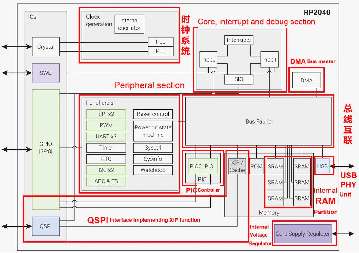
We can think of a chip as a "miniature factory", where each module in the diagram corresponds to a distinct "workshop / post": some are responsible for computation, some for data transmission, and others for interfacing with external devices. These posts work in tandem to enable the chip to fulfill tasks such as control and arithmetic operations. Below, we will explain the function of each "post" according to the partitions in the diagram:
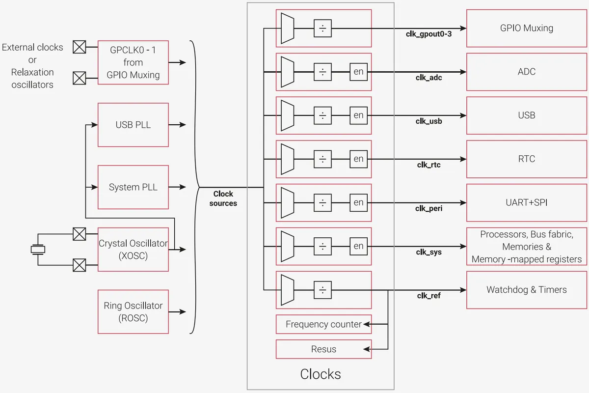
Clock system: It acts as the "metronome" of a factory — responsible for generating a stable "time rhythm"(for example, internal oscillators and external crystal oscillators provide the basic beat, while the PLL module speeds up the beat to 133MHz), ensuring that all modules operate in a synchronized rhythm (for instance, timing a 1-second blink for an LED relies entirely on this beat to calculate time).
Kernel, Interrupt and Debugging Components: They function as the "core workers" of the factory — Proc0 and Proc1 are the two "workers"(dual-core) responsible for executing programs and handling core tasks; the SIO acts as the "tool workshop for the workers", enabling data exchange between the two; Interrupts serve as the "emergency caller" that can interrupt the workers’ ongoing tasks to prioritize urgent ones when sudden tasks arise (such as an unexpected sensor trigger); the SWD is the "supervisor interface" that allows checking the workers’ working status and identifying the root causes of task errors.
DMA bus master: It acts as the "porter" in a factory — it handles data transfer for the core processing units (for example, moving sensor data from peripherals to memory), so that the processing units do not need to perform these routine data transfer tasks themselves, and can focus on core processing work to improve overall efficiency.
Bus Fabric: It serves as the "internal pathway" of the factory — all communication and data transmission between modules are carried out through this "pathway", ensuring efficient interconnection between all workstations.
Internal RAM Partition: It acts as the "temporary warehouse" of the factory — the 264KB SRAM is divided into 6 separate "sub-warehouses" that can store different types of temporary data simultaneously (for example, Worker A uses Warehouse 1, while the porter uses Warehouse 2), which prevents space conflicts between different tasks and improves the efficiency of data access.
Peripheral Section: It serves as the "external interface" of the microcontroller — it consists of modules including SPI/I2C/UART (the "communication interfaces" for interacting with external devices), PWM (the "regulator" for dimming lights or controlling motors), ADC & TS (the "measuring instruments" for detecting voltage and temperature), and is responsible for connecting and interacting with external components such as sensors and LEDs.
PIO controller: It serves as the "universal workbench" for factories — it supports custom interface functions (such as emulating SD cards and VGA interfaces) to expand the peripheral capabilities that the chip does not natively have.
The QSPI interface implements the XIP function: it acts as the "direct access channel from the external warehouse" for the factory — by connecting to external flash memory (equivalent to a "large external warehouse") via the QSPI interface, the XIP function enables the chip to read programs directly from the external warehouse without first transferring them to the internal temporary storage, thus saving internal space.
USB PHY Unit: It acts as the "USB express interface" of the factory — responsible for communicating with external USB devices (computers, USB flash drives) to enable program downloading and data transmission.
Internal Voltage Regulator: It acts as the "power supply stabilizer" of the chip — it stabilizes the externally input voltage and converts it into the 1.1V voltage required by the chip core, ensuring stable power supply for all modules.
XIP / Cache : The microcontroller connects to an external NOR QSPI FLASH via a dedicated SPI, DSPI or QSPI interface to implement the XIP (eXecute In Place) function, and a small cache can improve the performance of typical applications;
SWD Debug Interface: The SWD debug interface is connected to the core;
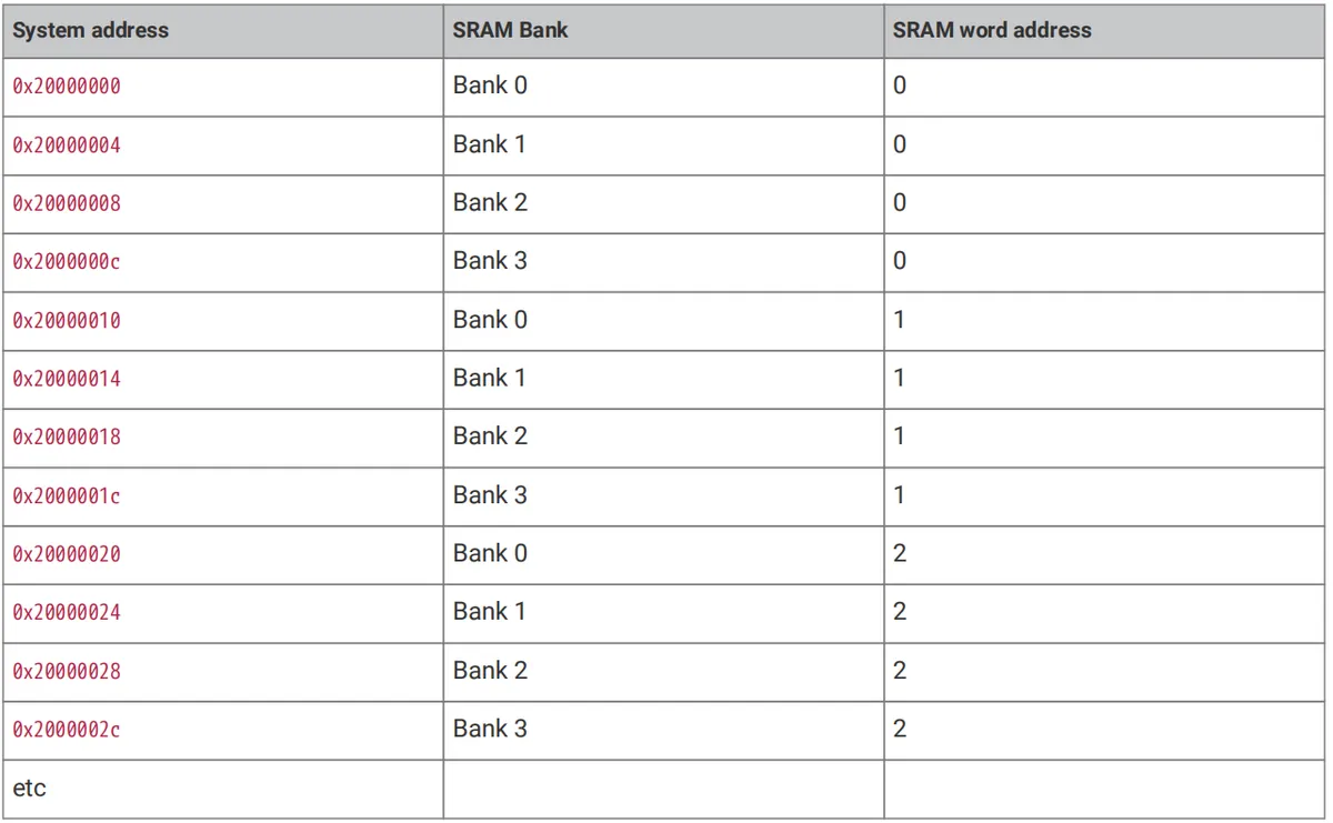
Internal SRAM Partition: The internal SRAM can store code or data. It is mapped as a single 264kB address space, but physically divided into 6 banks to enable simultaneous parallel access from different host buses — for example, the CPU can access one bank while the DMA accesses another;
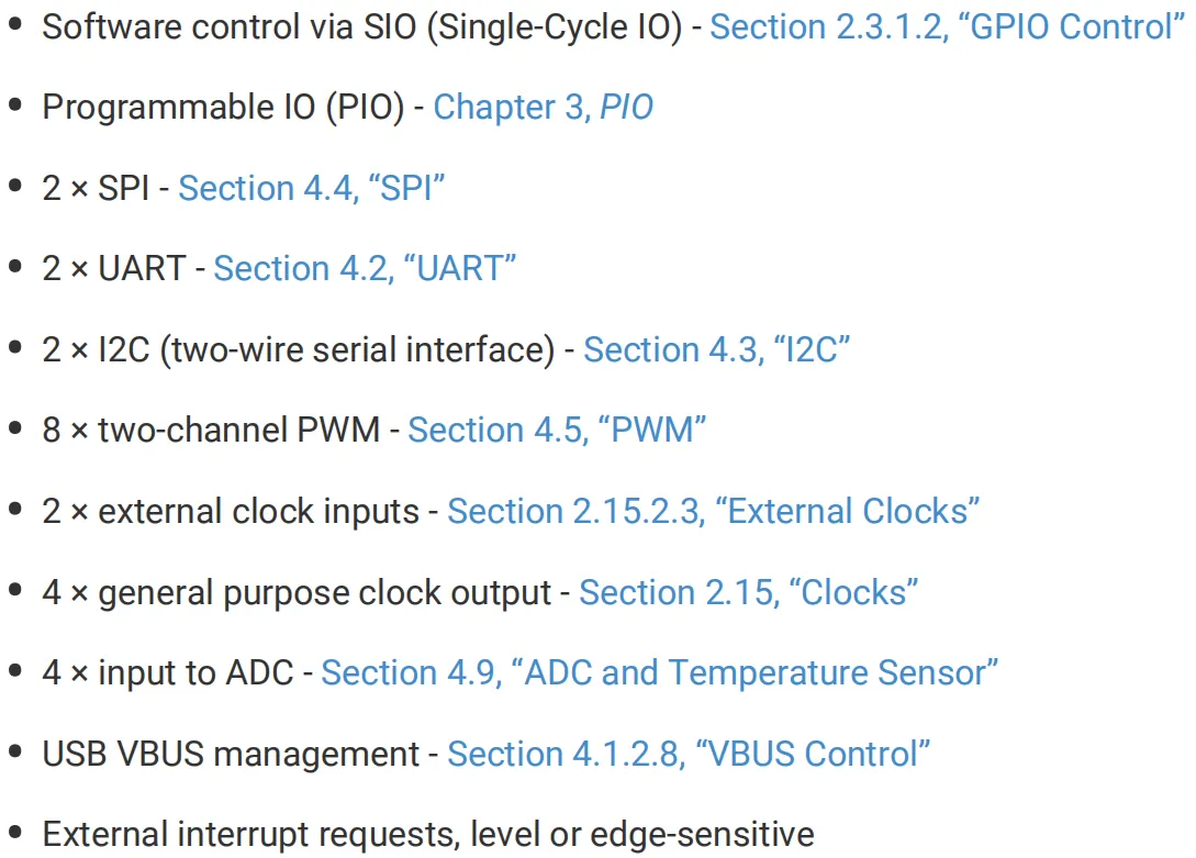
GPIO Ports and Peripherals: GPIO pins can be directly driven, or work with peripherals to implement multiplexing functions such as SPI, I2C, and UART.
PIO Controller: The flexible and configurable PIO controller can be used to provide various IO functions.
USB PHY Unit: The USB controller with an embedded PHY can be used to provide FS/LS host or device connections under software control
Clock System: Two PLLs (Phase-Locked Loops) provide a fixed 48MHz clock for USB or ADC, as well as a flexible system clock up to 133MHz.
Internal Voltage Regulator: An internal voltage regulator is provided to supply the 1.1V core voltage
DMA Bus: A DMA bus master can be used to offload repetitive data transfer tasks from the processor
Kernel Part: two completely symmetric processing cores, namely Proc0 and Proc1
2.2 Pin Mapping
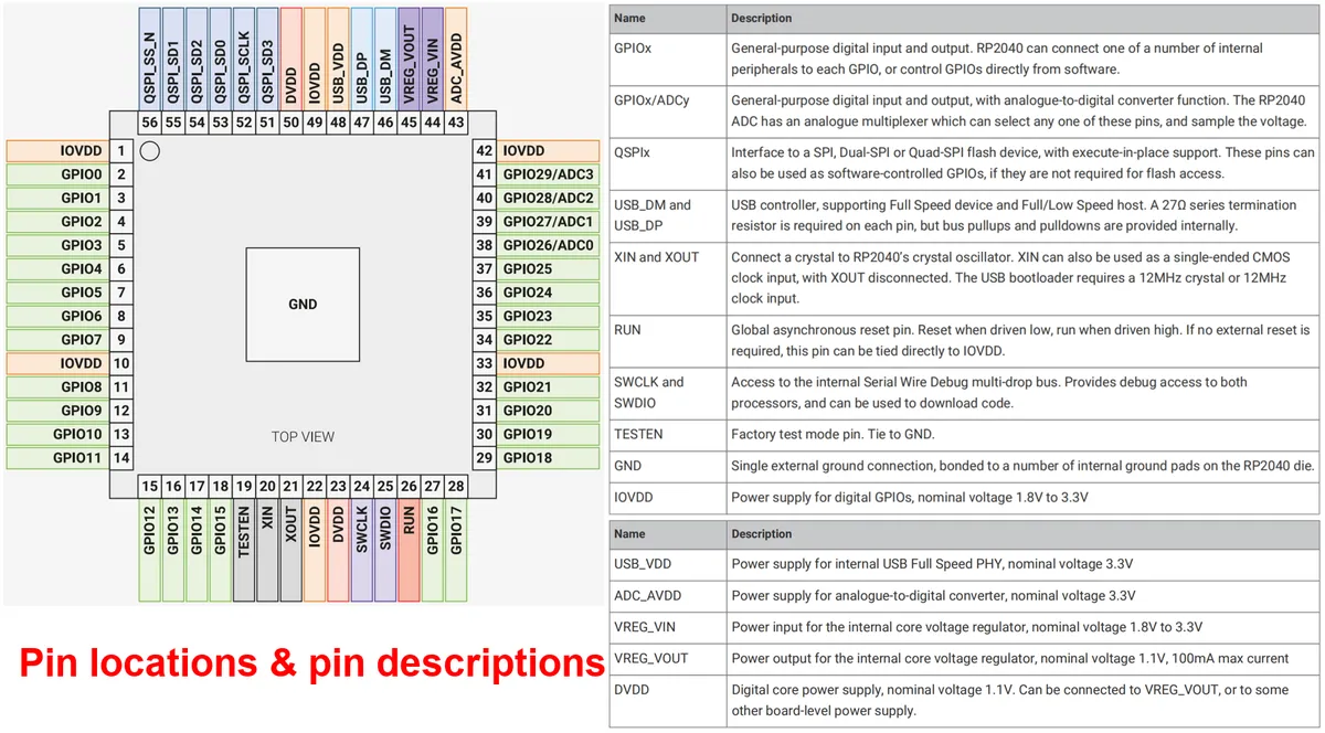
For chip learning, pin mapping serves as the critical link between "the internal functions of a chip" and "the actual physical hardware" — it is a "wiring guide" that creates a one-to-one correspondence between the functional modules in the chip block diagram (such as GPIO, ADC, UART) and the physical pins on the chip package (i. e., the exposed metal legs of the chip).
The reason why it is necessary to understand the pin mapping is as follows:
It serves as the "operation manual" for hardware design: the block diagram tells you that the chip has functions such as GPIO and ADC, but the pinout will clearly specify "which physical pins on the chip these functions correspond to specifically" — for example, if you want to connect a temperature and humidity sensor (using I2C) to the RP2040, you have to find the physical pins that support the I2C function through the pinout before you can solder and wire correctly;
It serves as the "function index" for program development: when writing a program to control a certain function (such as turning on an LED), you need to determine the "pin number corresponding to that function" through pin mapping, so as to correctly configure the pin in the code;
It serves as a "reference sheet" for function multiplexing: many pins support multiple purposes (for example, the GPIOx pins of the RP2040 support ADC functionality at the same time), and the pinout will mark the multiplexing function of each pin, making it convenient for you to select the appropriate pins according to your project requirements.
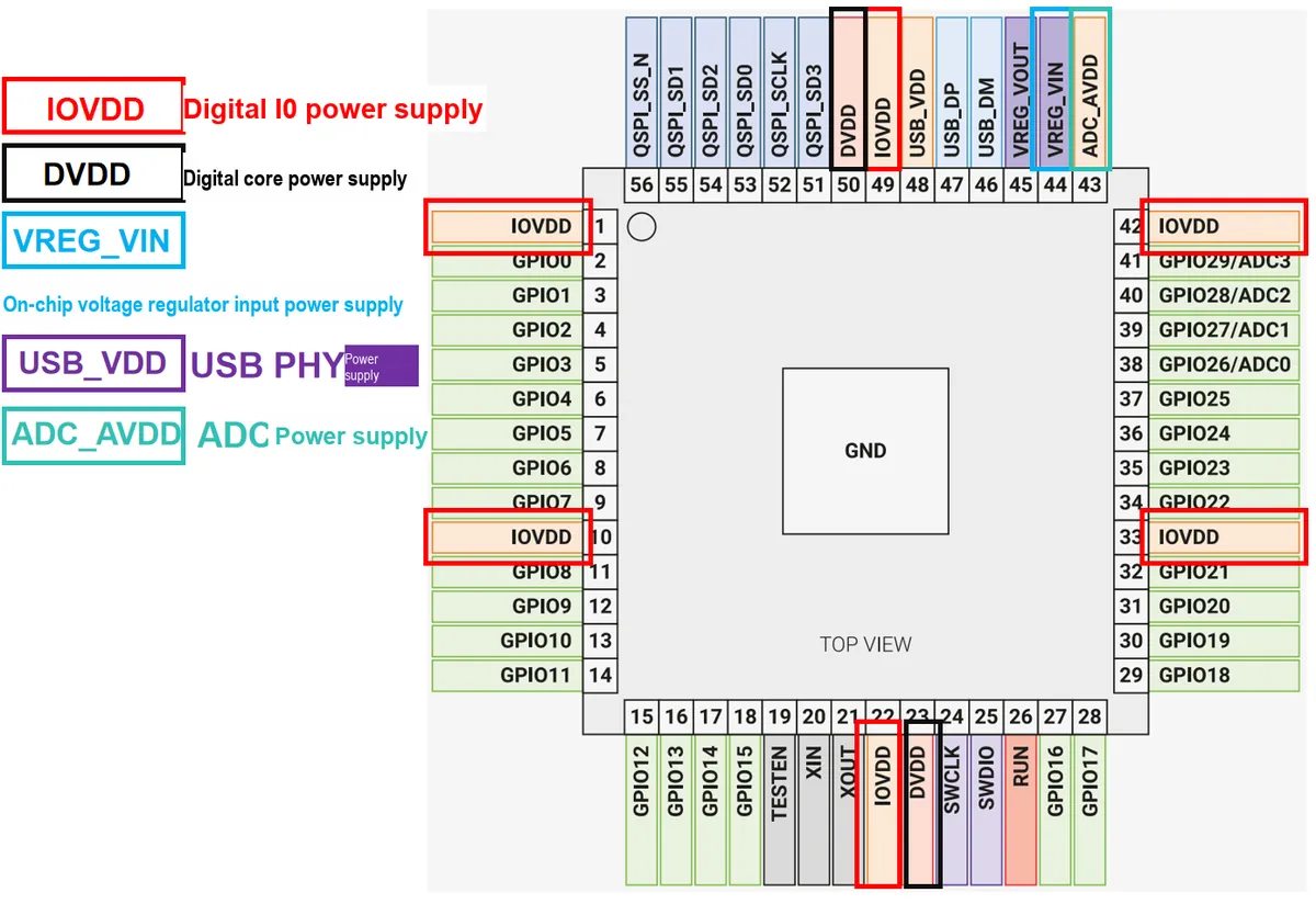
Figure 2.5 RP2040 Chip Pin Mapping and Function Description
Take the pinout diagram of this RP2040 as an example: the left side of the diagram shows the physical pin numbers of the chip, while the right side lists the corresponding functions of each pin (for instance, GPIO029/ADC3 means "physical pin 42 corresponds to the GPIO29 function and also supports ADC3 acquisition"). Only by mastering this can you translate the understanding you gained from the block diagram that "there are GPIO and ADC functions" into actual hardware connections and program development — this is also the necessary step when learning any chip, moving from "architecture awareness" to "practical application".
2.3 Pin Multiplexing Function
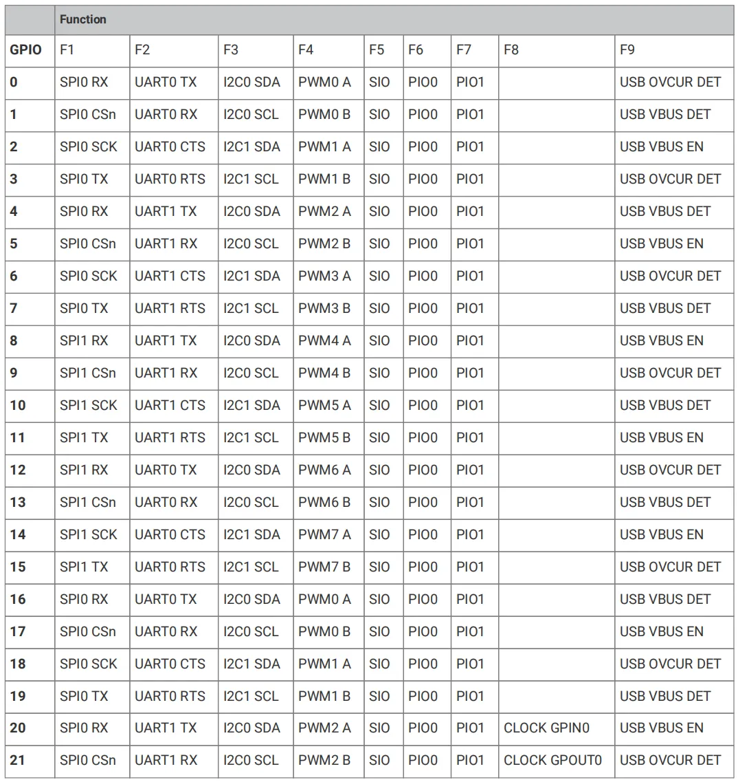
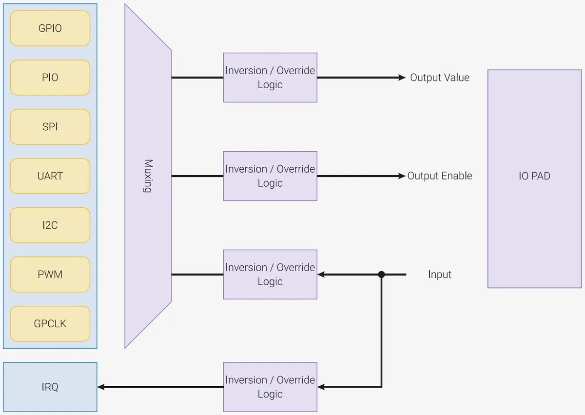
Put simply, pin multiplexing means "a single GPIO pin can serve multiple roles" — for instance, one GPIO pin can function as an ordinary switch (controlling the on/off state of an LED), be switched to act as an "SPI interface"(to connect to a sensor), or be configured as a "UART interface"(to connect to a serial port). Just like a smartphone's Type-C port that can charge the device, transfer data, and connect to other peripherals, realizing multiple functions through one single port — this is exactly what "multiplexing" refers to.
Each individual GPIO pin can be connected to an internal peripheral via the GPIO function defined below:
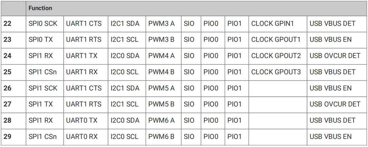
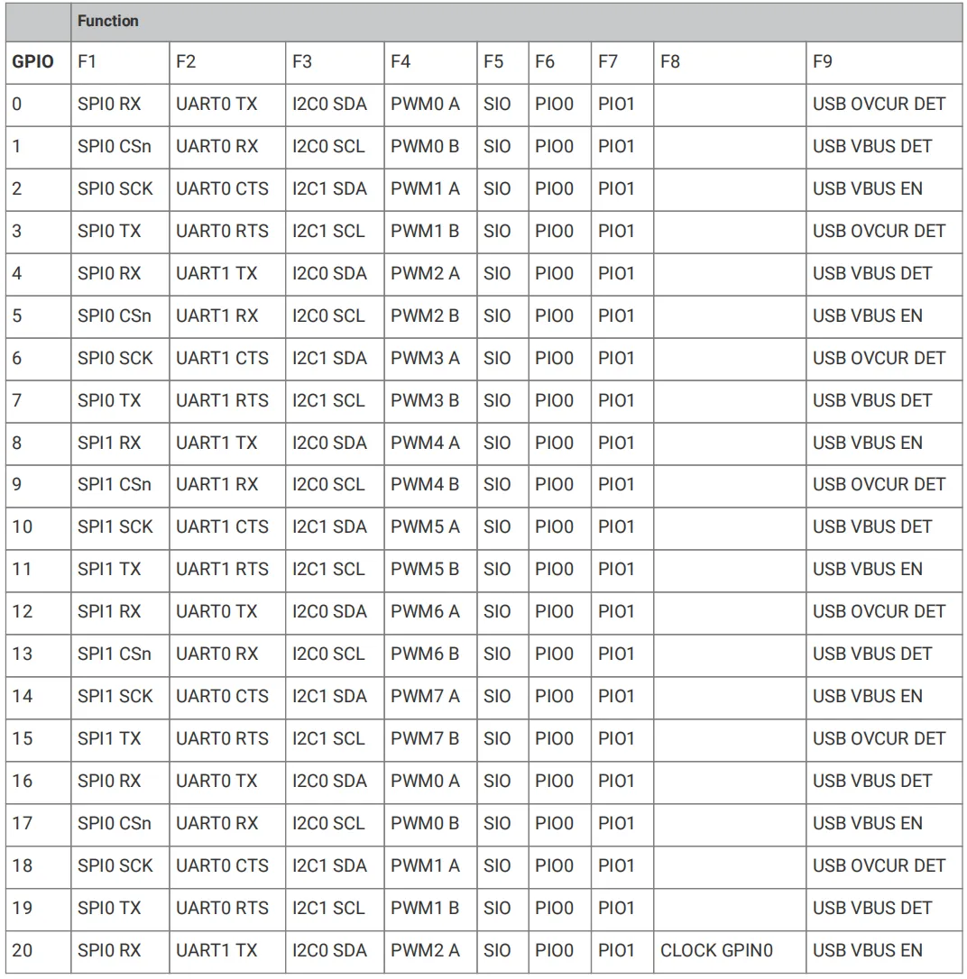
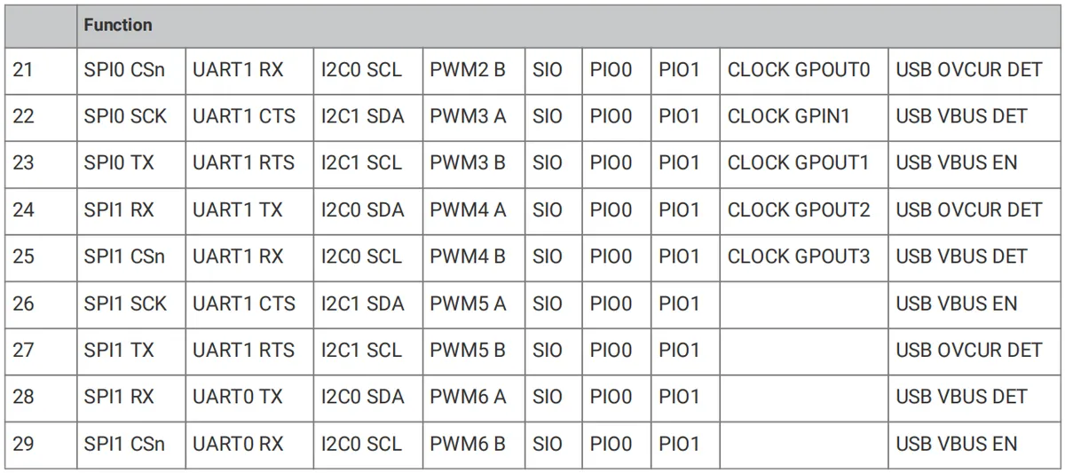
Figure 2.6 RP2040 GPIO Pin Multiplexed Function Table (0-21)Figure 2.7 RP2040 GPIO Pin Multiplexed Function Table (22-29)
This table is the " GPIO 'Function Selection Table'", and its structure and usage are very simple:
First column (GPIO number): indicates the specific GPIO pins (e. g., GPIO0, GPIO1), and each pin corresponds to one row;
Columns F1 to F9 (function options): refer to the "roles" that this GPIO can switch between (for example, F1 corresponds to SPI0 RX, and F2 corresponds to UART0 TX) — each GPIO can select one function from these options for use (only one function can be selected at a time);
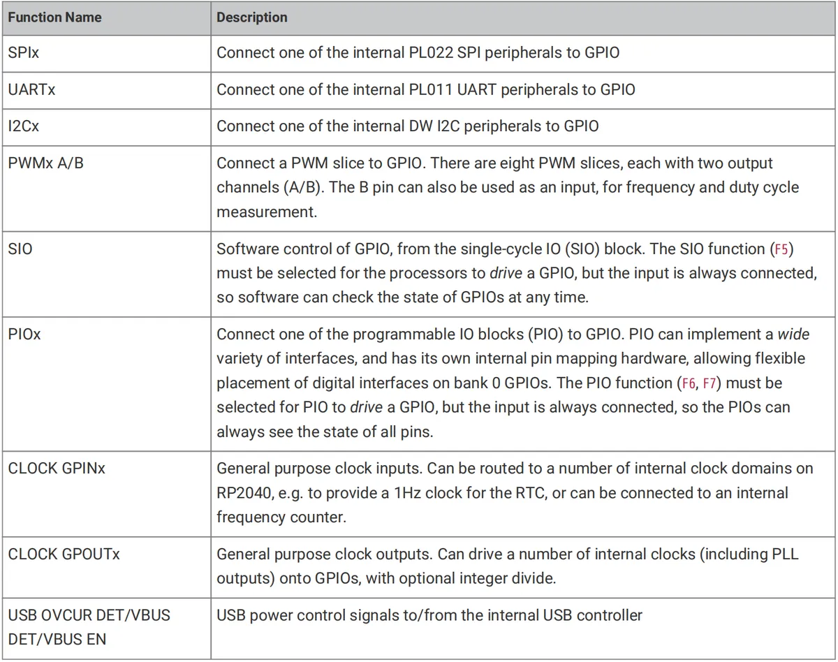
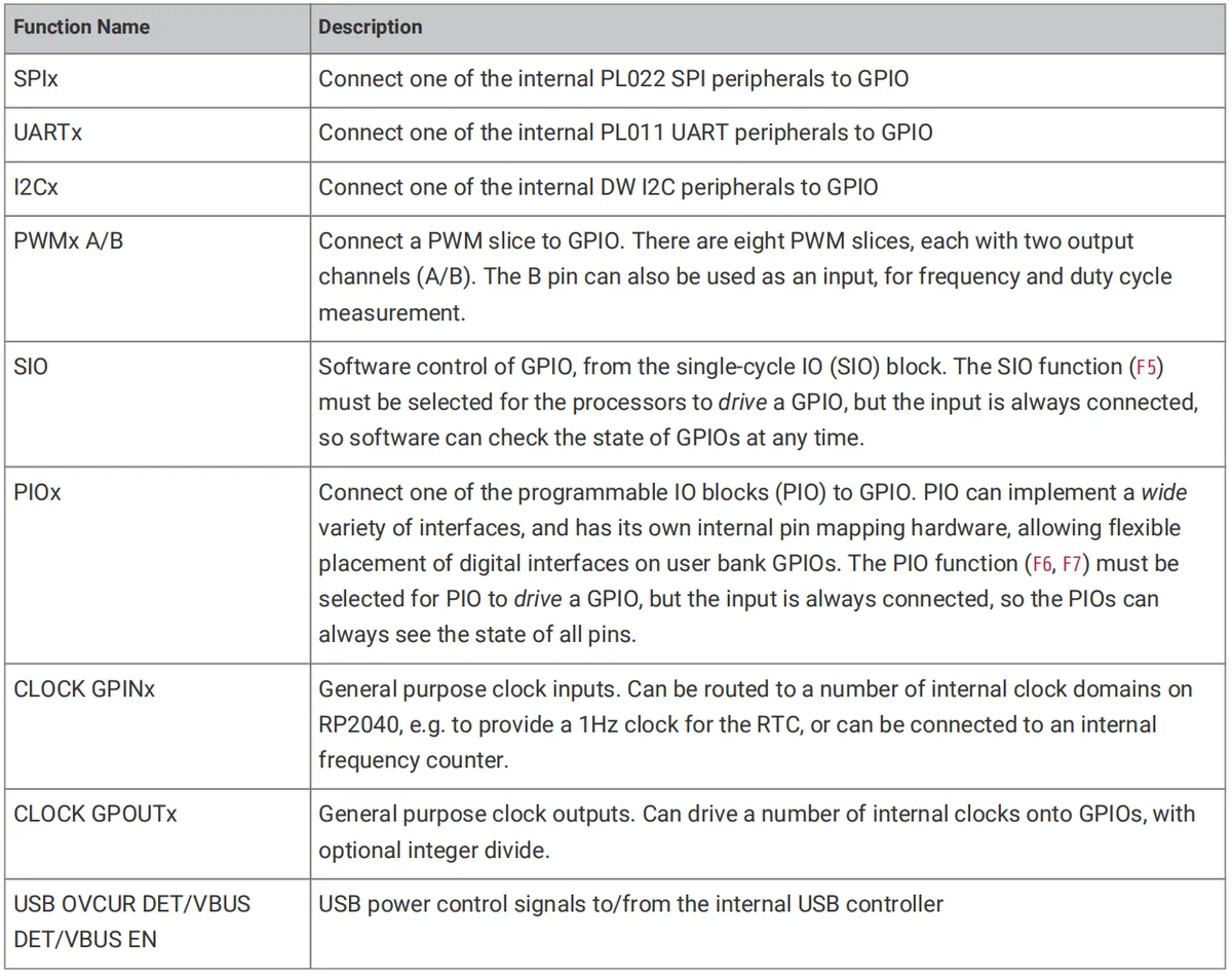
Figure 2.8 RP2040 Pin Multiplexed Function Description Table
The function description table above explains the internal components of the chip corresponding to each "role"(for example, SPIx corresponds to the SPI controller inside the chip, and UARTx corresponds to the UART controller), as well as the purpose of each function.
2.4 Brief Introduction to System Characteristics and Architecture
2.4.1 Bus Interconnection Architecture
The bus interconnection structure is the "data transportation system" inside a chip — it governs how data and instructions are transmitted between various functional modules (cores, memory, peripherals), making it one of the core architectures that impact a chip's operating efficiency. Understanding it clarifies how the chip "avoids data transmission congestion" and the "communication priorities of different modules", which is the key to grasping the chip's performance bottlenecks and resource scheduling logic.
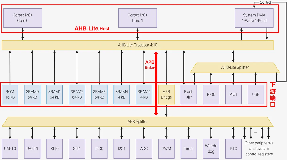
Figure 2.9 RP2040 Chip Bus Interconnect Block Diagram
This diagram illustrates the "internal communication network" of the RP2040, with the core logic as follows:
AHB-Lite Master (Upstream Port): It is the initiator of data requests, corresponding to 4 traffic initiators — two processor cores (Core0, Core1), the read port of DMA, and the write port of DMA, which are responsible for sending read/write data requests to other modules.
AHB-Lite Crossbar (bus hub): it acts as a "traffic control center", which distributes requests from 4 master devices to 10 "downstream ports"(i. e., the modules to which data is to be delivered); it can complete up to 4 transmissions of 32-bit data per cycle, ensuring the efficiency of data interaction.
Downstream port (destination module): refers to the recipient of a data request, which falls into three categories:
Memory Class Module: It consists of ROM, Flash XIP, and the partitioned SRAM0 to SRAM5 (each SRAM occupies an independent port). Splitting the SRAM into multiple ports is designed to enable "multi-module parallel access" — for example, while Core0 is accessing SRAM0, the DMA can access SRAM1 simultaneously — so as to prevent access congestion of memory resources.
High-speed peripheral modules: including "Fast AHB-Lite peripherals" such as PIO0, PIO1, USB, etc. , which are directly connected to the bus hub to adapt to the requirements of high-speed data transmission.
Low-speed peripheral modules: These include peripherals such as UART, SPI, and I2C, which are connected to the bus hub via an "APB bridge" — the APB bridge acts as a "slow lane adapter", ensuring that communications from low-speed peripherals do not compromise the transmission efficiency of high-speed modules.
2.4.2 Address Mapping
To understand address mapping, we must first clarify its core definition: Address mapping refers to the rules by which a chip assigns unique "numeric addresses" to all its internal resources, including ROM, SRAM, and peripheral registers. It is equivalent to assigning a "house number" to every memory block and functional module inside the chip; modules such as the core and DMA can precisely locate and access the corresponding resource via this "house number", i. e., the address.
The reason why address mapping is required is that the arithmetic/control modules of the chip (such as dual-core processors and DMA) can only locate resources through "addresses": for example, when the core needs to read data from the SRAM or configure the communication parameters of the UART, it must first find the storage area of the SRAM and the control registers of the UART via the corresponding addresses — without address mapping, these modules are just like "rooms without house numbers" and cannot be located or accessed at all. The essence of address mapping is to establish a "unique accessible identifier" for resources, which serves as the basic rule for internal communication within the chip.
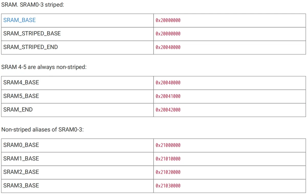
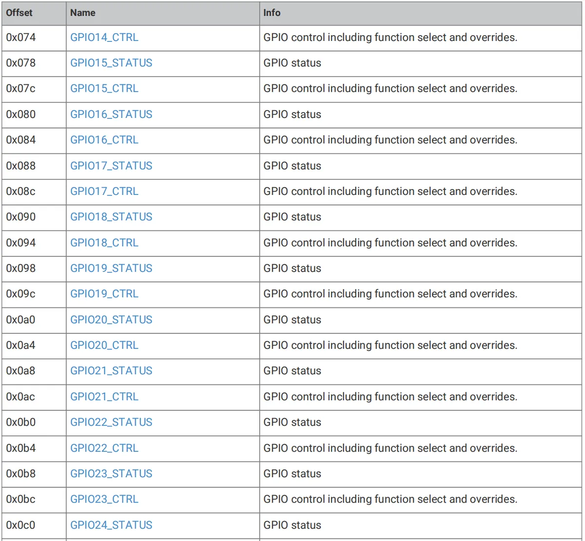
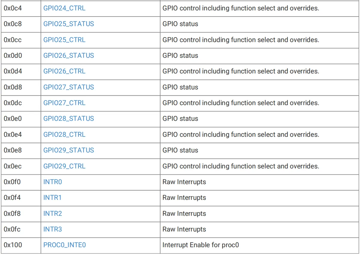
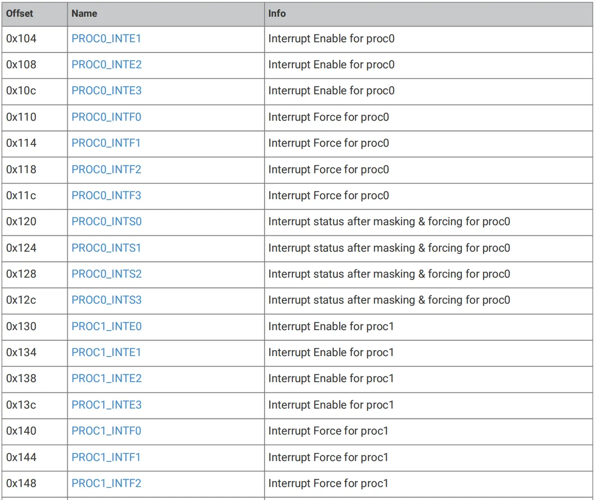
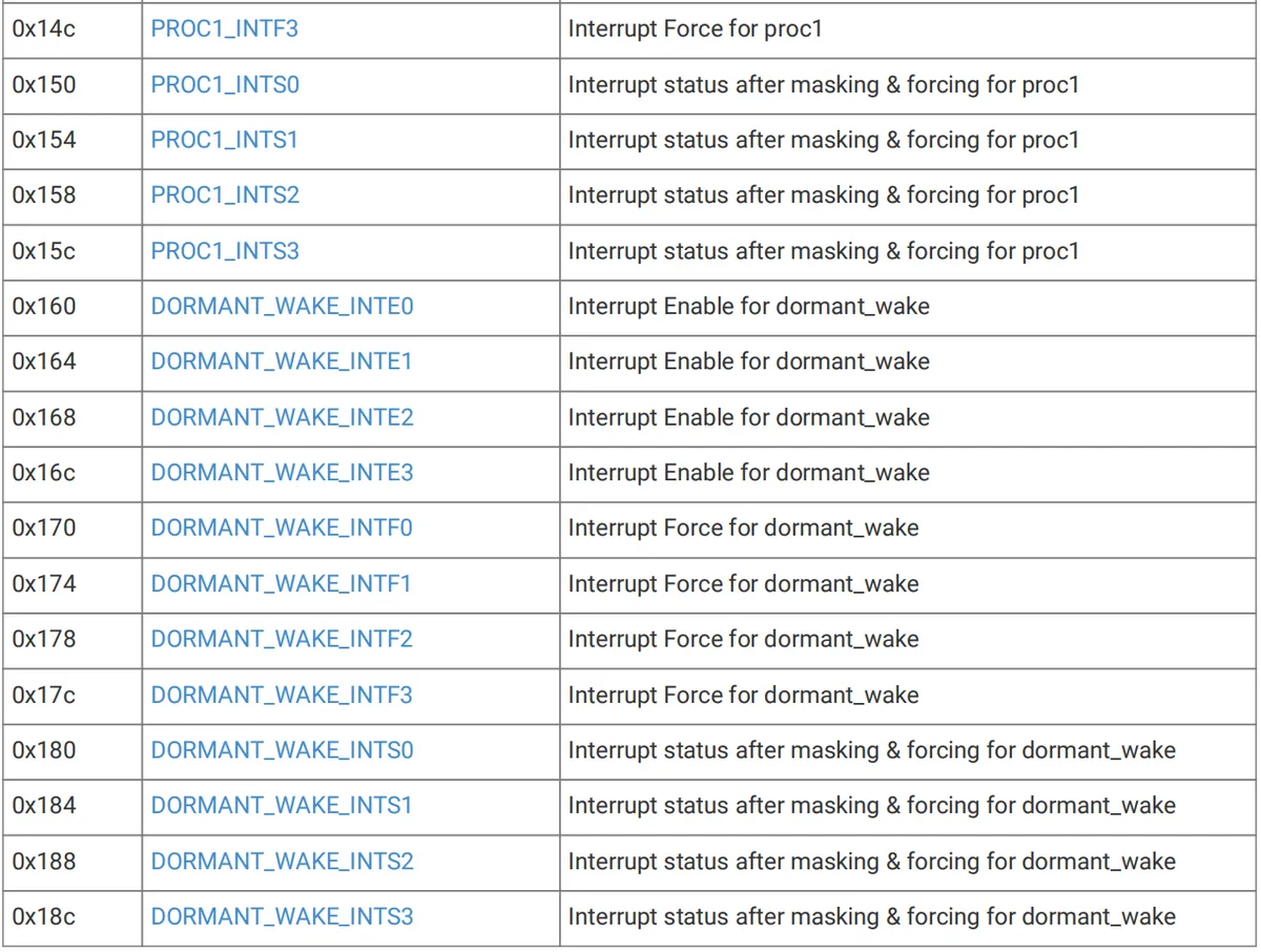
And the address mapping works in deep coordination with the aforementioned "SRAM partitioning" — take the SRAM of the RP2040 as an example: As previously mentioned, the SRAM is physically divided into 6 banks (SRAM0 to SRAM5), which is designed to support "parallel access" by multiple modules (for instance, while Core0 is accessing SRAM0, the DMA can access SRAM1 simultaneously);The address mapping table assigns separate address ranges to these 6 banks (for example, SRAM0_BASE is 0x21000000 and SRAM1_BASE is 0x21010000).
As a result, when Core0 accesses addresses starting at "0x21000000", they actually map to the physical SRAM0; when the DMA accesses addresses starting at "0x21010000", they correspond to the physical SRAM1 — address mapping enables different modules to access "distinct physical partitions" via "different house numbers", which not only achieves precise resource positioning but also realizes "parallel access" in coordination with the physical partitions of SRAM, avoiding resource conflicts between modules and improving data access efficiency.
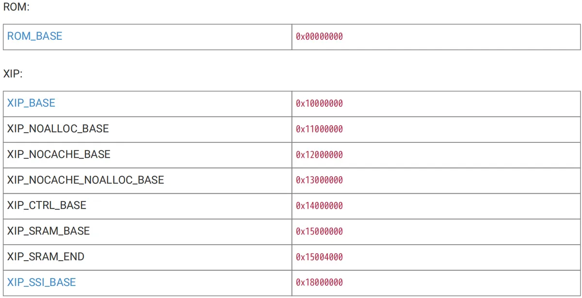
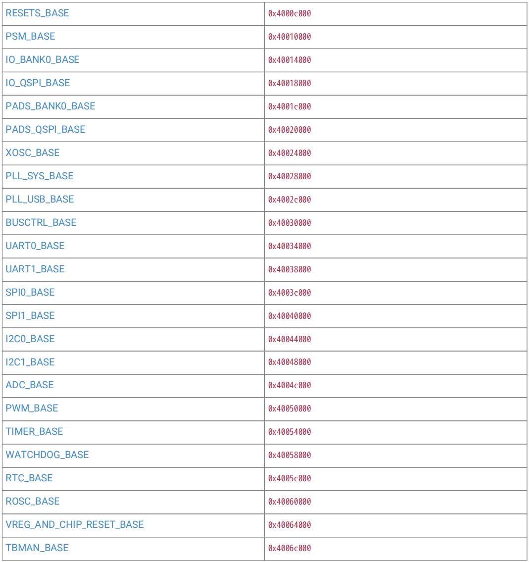
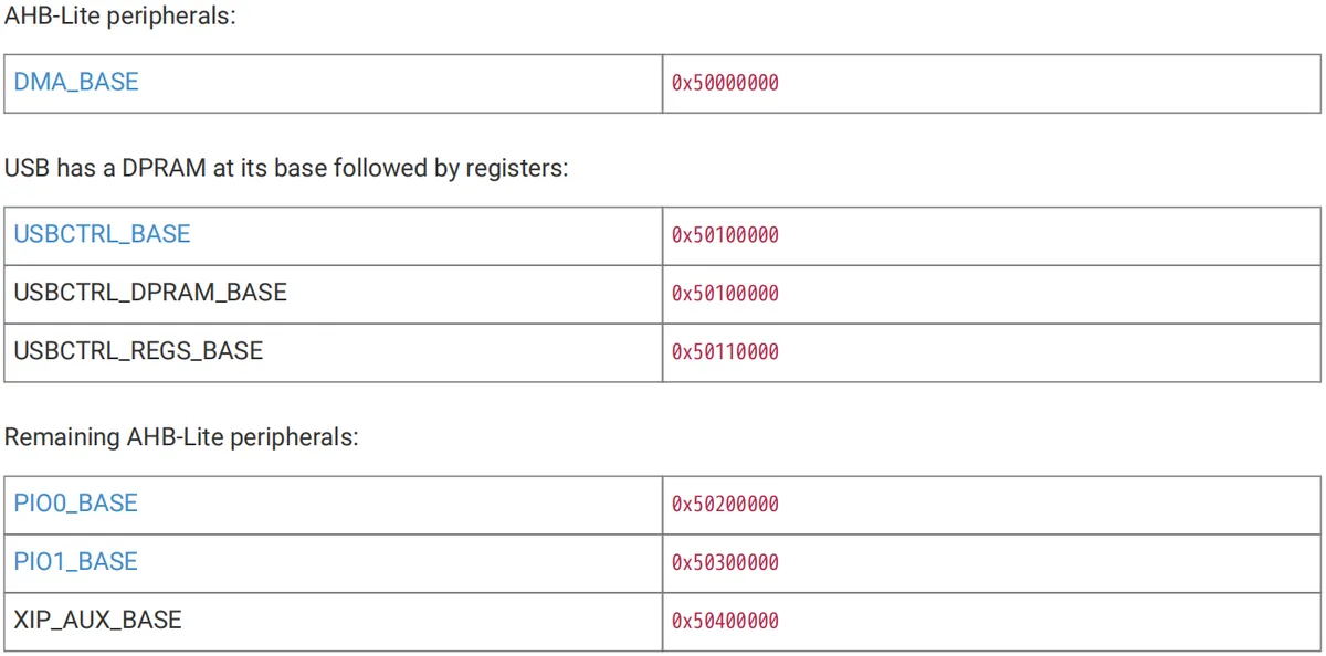
The address mapping of RP2040 is as follows:
IOPORT Peripherals:
Figure 2.10 RP2040 Chip Address Map (Full Series)
As can also be seen from the address mapping table in the figure:
Different types of resources are allocated to distinct address ranges (for example, ROM starts at 0x00000000, SRAM at 0x20000000, and peripherals at 0x40000000), which makes it easier for modules to distinguish whether the target to be accessed is a memory or a peripheral.
Different sub-modules of the same type of resource (e. g., SRAM0 to SRAM5) have consecutive yet independent address ranges, which not only ensures the integrity of the storage but also supports partitioned access.
2.4.3 Processor Subsystem
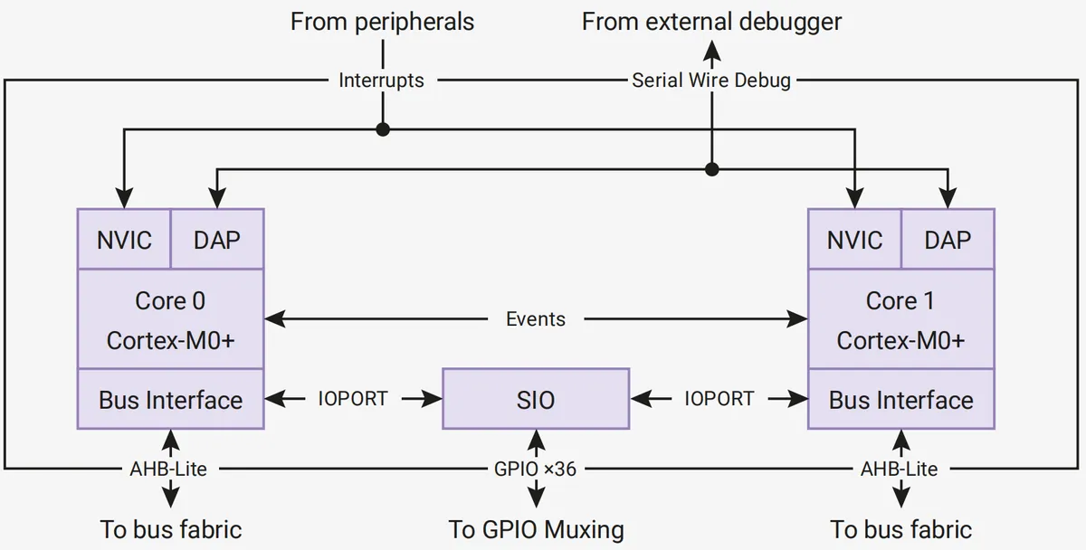
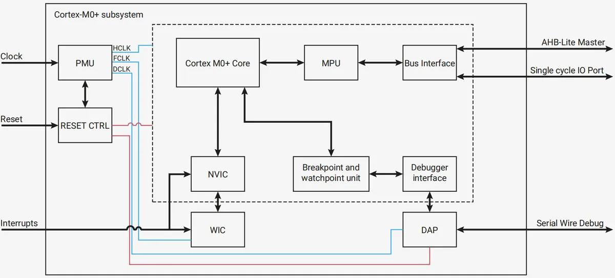
The RP2040 processor subsystem consists of two Arm Cortex-M0+ processors — each equipped with its standard internal Arm CPU peripherals as well as external peripherals for GPIO access and inter-core communication.
The diagram above illustrates the "working connection framework" of the RP2040 dual-core processor — it defines the communication modes between the two Cortex-M0+ cores (Core0, Core1), other on-chip modules and external devices, serving as the fundamental supporting structure for dual-core collaborative work. The functions of the core communication interfaces are as follows:
Independent AHB-Lite Bus Interface: Each core is equipped with a dedicated 32-bit AHB-Lite bus, which serves as its "exclusive main artery" for accessing memory and peripherals — for instance, when Core0 reads SRAM programs or Core1 configures UART peripherals, both connect to the Bus Fabric via their respective buses. This independent bus design eliminates "traffic congestion and resource contention" when the dual cores access resources, ensuring efficient read and write operations for code and data.
SIO Block and IOPORT: High-Speed GPIO Access + Dual-Core Collaboration SIO is a "high-speed interface block" dedicated to dual-core systems, with each core connected to the SIO via an IOPORT:
On the one hand, it provides "high-speed, latency-free access" to GPIO — this method delivers faster response and more stable timing compared to accessing GPIO via a bus (for example, it can ensure precise rhythm when quickly controlling LED blinking);
On the other hand, the SIO is also responsible for "Events communication" between the two cores, enabling Core0 and Core1 to send signals to each other (for example, after Core0 completes Data Acquisition, it sends an event to notify Core1 to perform processing), thus realizing dual-core collaboration.
Interrupt System: Divided Response to Spontaneous Tasks Peripherals (such as sensor triggers, UART data reception) generate interrupt signals, which are routed to the NVIC (Nested Vectored Interrupt Controller) of the two cores. The 26 system-level interrupts of the RP2040 can be assigned to either core for processing — for example, the interrupt for "UART data reception" can be allocated to Core 0, and the interrupt for "sensor trigger" to Core 1, enabling the dual cores to respond to sudden tasks in a divided manner and improving the real-time performance of the system.
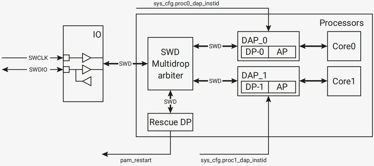
SWD Debug Bus: A Unified Entry Point for External Debugging An external debugger connects to the DAP modules of both cores simultaneously via a multi-drop Serial Wire Debug bus — this means the external debug host can access and debug Core0 and Core1 at the same time. For example, when a program malfunctions, it is possible to view the running status of both cores concurrently to accurately locate issues in dual-core collaboration.
Next, we will introduce these key components one by one.
2.4.3.1 Single-cycle IO block (SIO)
SIO is the "high-speed collaboration toolbox" for the dual-core RP2040 processor — it leverages the IOPORT auxiliary bus of the Cortex-M0+ to achieve "single-cycle (ultra-fast)" operations, and is specifically designed to handle tasks with strict speed and timing requirements such as "high-speed data transfer between dual cores", "contention for shared resources", and "high-speed GPIO control", serving as the core supporting module for efficient dual-core collaboration.
The essence of SIO is a "fast lane module" based on the IOPORT auxiliary bus: IOPORT is a dedicated fast bus port of Cortex-M0+, corresponding to the address range starting from 0xd0000000, which can be accessed with ordinary read and write instructions. Moreover, SIO is not connected to the main system bus and only uses this fast channel — this ensures that all read and write operations of SIO can be completed within 1 cycle, featuring high speed and precise timing.
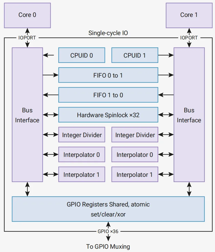
The specific structure of SIO is shown as follows:
SIO performs 32-byte accesses by leveraging the auxiliary bus IOPORT of the Cortex-M0, which is designed to save access time, execute high-speed computing tasks, and also serve as a communication channel between two cores.
IOPORT is an auxiliary bus port on the Cortex-M0+ that enables high-speed 32-bit read and write operations.
Processors access their IOPORTs using standard load and store instructions, targeting the dedicated IOPORT address range from 0xd0000000 to 0xdfffffff. The SIO appears as memory-mapped hardware within the IOPORT space.
SIO has a dedicated bus interface for each processor's IOPORT. Due to its strict timing requirements, SIO is not connected to the main system bus, and can only be accessed by the processor or a debugger via the processor debug port.
Read and write operations of SIO are both completed in one cycle, which consists of the following units:
Dual-core FIFO: Used to transfer data, messages or ordered events between two cores.
One of the FIFOs can only be written to by core 0 and read from by core 1.
The other one can only be written by core 1 and read by core 0.
CPUID: It is used to identify the currently working core. The CPUID register is the first register in the IOPORT space. When accessing this address, core 0 reads a value of 0, while core 1 reads a value of 1. The software determines which core it is running on during the initial boot process: both cores start running simultaneously, core 1 enters a deep sleep state, and core 0 continues to execute the main boot sequence.
Hardware Mutex Lock: It can be used to manage mutually exclusive access to shared software resources, and software interacts with each spin lock through one of the following operations
Read: to acquire the lock
Write: Release the lock
hardware division and interpolator
IO Shared Access Control
A Layman’s Explanation of SIO
The core functional units included in SIO all serve the purposes of "dual-core collaboration" and "high-speed operation":
Dual-core FIFO: It serves as a "high-speed express box" between the two cores
FIFO0 can only be written to by Core0 and read by Core1; FIFO1 can only be written to by Core1 and read by Core0.
Its function is to enable the dual-core to transmit data and messages quickly (for example, after Core0 processes the sensor data, it directly writes the data into FIFO0, from which Core1 can read it immediately) without going through the main bus, thus avoiding latency.
CPUID: The "Identification Badge" of Dual-Core Processors
Core0 reads this register and obtains "0", while Core1 reads it and obtains "1".
At startup, the two cores run simultaneously. When Core1 reads its own identifier as "1", it enters sleep mode, while Core0, which reads "0", executes the boot program. Through this "identity identifier", task division during dual-core startup is achieved to avoid conflicts.
hardware Mutex lock (spinlock): a "shared resource placeholder" for dual-core systems
When two cores need to access the same shared resource (such as the same memory block), use this lock: a "read lock" is equivalent to "occupying the resource", while a "write lock" is equivalent to "releasing the resource".
Ensure that only one core can use the shared resource at the same time to avoid data confusion.
Hardware Division & Interpolator: The "Fast Calculation Accelerator" for Dual-Core Processors
A hardware divider enables division operations to be completed within a single cycle (far faster than software-based computation); an interpolator is a piece of hardware that assists with interpolation operations.
Its function is to accelerate specific computing tasks and improve the core computing efficiency.
IO Shared Access Control: serves as the "high-speed control port" of GPIO
Accessing GPIO registers via SIO is a "single-cycle + atomic operation"(the operation will not be interrupted), which is faster and more precise than controlling GPIOs through the main bus.
Suitable for scenarios with strict requirements on GPIO timing (such as fast LED blinking control and high-frequency signal output).
2.4.3.2 Interrupt
Interrupts are the core mechanism of the RP2040 for handling "burst tasks" — for example, when a timer expires, data is received via a serial port, or a sensor triggers a signal, the core cannot wait to "finish the task at hand" before handling these events; at such times, an interrupt will "interrupt" the core's current operation to prioritize the urgent task. Meanwhile, the NVIC (Nested Vectored Interrupt Controller) acts as the "interrupt dispatcher" for each core, responsible for managing interrupt priorities and execution sequences, and its logic will be clearly explained below with reference to the table and relevant rules:
IRQ and Priority
IRQ: short for "Interrupt Request", is an "urgent call signal" sent by peripherals (such as timers and UARTs) to the processor core. When a peripheral needs the core to process a task immediately — for example, when a timer expires or data is received via a serial port — it triggers the corresponding IRQ, prompting the core to suspend its current work and prioritize handling this urgent task.
Priority: refers to the sorting rule for the urgency of interrupt tasks. A chip may receive multiple IRQs at the same time, and tasks with higher priority will be processed first by the core to prevent urgent tasks from being delayed.
Each core (Core0 and Core1) has an independent NVIC, which acts as a dedicated "interrupt dispatcher" and can receive 32 interrupt signals. However, the RP2040 only uses the first 26 of these (IRQ0 to IRQ25), while the remaining IRQ26 to IRQ31 are reserved (though they can also be forcibly triggered). When a peripheral (such as a timer or UART) triggers an urgent task, it sends a signal to the corresponding IRQ, and the NVIC then schedules the core to process it.
On the RP2040, only the lower 26 IRQ signals are connected to the NVIC, while IRQs 26 to 31 are not tied to any source. By writing to bits 26 to 31 in the NVIC ISPR register, the core can still be forced to enter the corresponding interrupt handler.
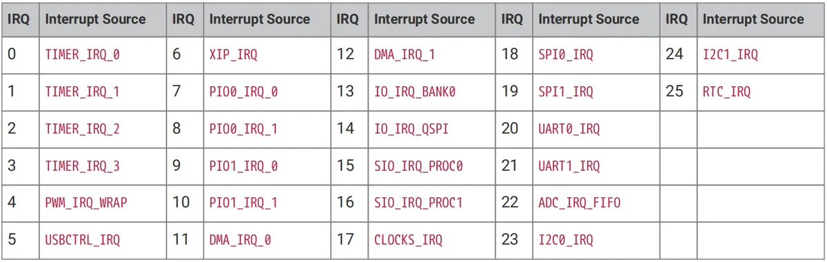
The interrupt vector table of the RP2040 is as follows. This table acts as the "task list for IRQs", where each IRQ number corresponds to a specific "source of urgent tasks":
Figure 2.13 RP2040 Interrupt Sources and IRQ Mapping Table
For example, IRQ0 corresponds to "the IRQ of Timer 0"(meaning Timer 0 has reached its set time), and IRQ20 corresponds to "the IRQ of UART0"(meaning UART0 has received data). Once the core sees the IRQ number, it can immediately identify which peripheral has sent this "urgent call" and then invoke the corresponding handler.
When multiple IRQs are triggered simultaneously, the core processes them in sequence according to their "urgency level", with priority determined in two layers:
NVIC dynamic priority: Each IRQ can be assigned 4 priority levels (0 to 3) via registers, where a smaller number indicates a higher urgency level (for example, level 0 is the highest priority and will be processed before level 1);
IRQ Number Priority: If two IRQs share the same NVIC priority, the IRQ number will be used as the tiebreaker — the smaller the number, the higher the urgency (e. g., IRQ0 has higher priority than IRQ1).
Support for nested interrupts in hardware: a low-priority interrupt can be preempted by a high-priority interrupt (or another exception such as a hard fault), and the low-priority interrupt will resume once the high-priority exception is completed. This "cutting in line" mechanism ensures that the most urgent tasks are always responded to first.
2.4.3.3 Event Signals
First, let's clarify the core concepts:
Event signal: A lightweight "wakeup/notification signal". The difference between it and an interrupt is that an interrupt "preempts the core's current task" to handle an urgent job, whereas an event mainly "wakes up a sleeping core" or "sends a notification to another core" and will not actively interrupt the core's execution.
WFE instruction: short for Wait For Event. After executing this instruction, the core will enter a sleep state and suspend its operation, and will not be woken up until an event or interrupt arrives.
SEV instruction :The full name is Send Event. Executing this instruction on the core can actively generate an event signal to notify or wake up other cores.
In the RP2040, the event signal serves as the core mechanism for dual-core coordination and low-power sleep, with its logic outlined as follows:
Event intercommunication between dual cores:
The event signaling between the two cores (Core0 and Core1) of the RP2040 is "cross-connected" — for example, when Core0 executes the SEV instruction to send an event, this event will be received by Core1; conversely, events sent by Core1 can also be received by Core0.
The purpose of this design is to implement "lightweight notification between dual cores": for example, after Core0 completes Data Acquisition, it sends an event to wake up Core1 which is in sleep state to let it continue processing data. This not only avoids the waste of computing power caused by idle waiting of the core, but also is more lightweight than using interrupt for notification.
Implementation of low-power sleep mode:
After the core executes the WFE (or WFI, Wait For Interrupt) instruction to enter the sleep state, the internal clock gate of the core will be turned off and no additional power will be consumed; if both cores enter the sleep state and the DMA is also inactive, the entire RP2040 will enter "global sleep", which simultaneously turns off the clocks of unused modules to further reduce power consumption.
The trigger conditions for wake-up are highly flexible: whether it is an event sent by another core or an interrupt triggered by a peripheral, it can wake the core (or the entire chip) from sleep and resume operation — this is extremely practical in scenarios requiring low power consumption, such as battery-powered devices.
2.4.3.4 Debugging
Before understanding the debugging structure, let's first clarify several core concepts:
SWD (Serial Wire Debug): a debug interface that requires only two wires (the SWCLK clock line and the SWDIO data line). It acts as the "channel" for communication between an external debugger (such as a debugging tool on a computer) and the internal modules of a chip, and is used to implement operations including program downloading and debugging.
DAP (Debug Access Port): it serves as the "debugging entry point" inside the chip, and each core (Core0, Core1) corresponds to one DAP (DAP_0, DAP_1); an external debugger can access the operating status of the cores and control their execution via the DAP.
SWD Multi-Node Arbiter: It acts as the "traffic controller" for debug communication — the external debugger only has one SWD interface, yet it needs to connect to the DAPs of two cores and the backup rescue port; the arbiter is responsible for allocating communication resources to prevent signal contention from multiple debug access points.
Rescue DP (Debug Rescue Port): serves as the "safe exit" for debugging — when normal DAP debugging fails (e. g., the core is locked up), this backup port can be used to restore debugging functionality.
Figure 2.15 RP2040 SWD Serial Wire Debug Architecture Block Diagram
This diagram illustrates the debug communication architecture of the RP2040, which implements the unified control of dual-core by an external debugger plus debug reliability assurance, with the core logic as follows:
Basic Communication of the SWD Interface: An external debugger connects to the chip's IO module via the two lines SWCLK and SWDIO, and then accesses the SWD multi-node arbiter — this is the only communication channel between the debugger and the chip's internal circuitry. It is recommended to use a maximum frequency of 24MHz to ensure stable communication.
Debug Resource Scheduling (Role of the Arbiter): Since there are 2 core DAPs inside the chip (DAP_0 corresponds to Core0, DAP_1 corresponds to Core1) and 1 Rescue DP, while the debugger only has 1 SWD interface, the arbiter allocates communication to the corresponding port based on debugging requirements:
To debug Core0, allocate it to DAP_0;
To debug Core1, allocate it to DAP_1;
When normal debugging fails, it is allocated to the Rescue DP. This prevents multiple debugging entry points from contending for signals and ensures orderly communication.
Core Functions of SWD Debugging Through this architecture, an external debugger can perform the following operations:
Load a program (firmware) to the SRAM of the chip or an external flash memory;
View / modify the core operating status (e. g., register values);
Core Control Execution: It enables the core to run, stop, and execute code step by step, and also supports setting breakpoints (to pause the core when it executes to the specified code position).
The "rescue" guarantee of Rescue DP When normal DAP debugging becomes unavailable due to core lockup, configuration errors or other reasons, Rescue DP can serve as a backup entry to restore debugging functionality via the pam_restart signal — this is a safety mechanism to prevent the chip from being "bricked" due to debugging failures.
2.4.4 Cortex-M0+ Core
The core is the central processing brain of a microcontroller chip, and all program execution, data computation, and task scheduling of the chip are ultimately completed by the core, which directly determines the core capability boundaries of the chip (such as computing speed, power consumption level, and supported functions) and serves as the basis for judging "what scenarios the chip is suitable for"(e. g., low-power devices / complex computing devices) and "what tasks it can perform".
The ARM Cortex-M0+ processor is an ultra-low-power, low-cost microprocessor that supports the ARMv6M instruction set.
What is the ARM Cortex-M series?
This is the "microcontroller-specific core family" launched by ARM, which is divided into multiple models to meet different performance and power consumption requirements:
M0/M0+: Entry-level, low power consumption, and low cost (e. g., the M0+ used in RP2040), suitable for simple IO control and low-power devices;
M3/M4: mid-to-high-end models, supporting more complex operations (the M4 is equipped with a floating-point unit);
M7: High-end, suitable for high-performance scenarios.
The Cortex-M0+ is one of the models with "the lowest entry barrier and the lowest power consumption" in this family, focusing on basic control tasks featuring low cost and low power consumption.
The chip has the following features:
It adopts a 2-stage pipeline structure (instruction fetch + pre-decoding, decoding + execution);
Supports single-cycle I/O access:
"Single cycle" means that when accessing peripherals such as GPIO, a read or write operation can be completed in only one clock cycle;
With extremely fast IO access speed and ultra-low response latency, it is suitable for scenarios that impose strict requirements on IO timing, such as rapidly controlling LED blinking and high-frequency signal output.
Low power consumption with integrated sleep mode:
Sleep mode refers to a state in which the processor "temporarily suspends operation and reduces energy consumption": the core will turn off some circuits, lower the clock frequency, and only retain the necessary wake-up detection function;
Significantly reducing power consumption during chip idle periods is a core requirement for battery-powered devices such as smart bands and wireless sensors.
Capabilities featuring determinism, fixed latency, and interrupt handling:
"Determinism" means that the interrupt response time is fixed: regardless of what the processor is currently doing, the latency for processing an interrupt — the time from receiving the interrupt signal to starting to execute the interrupt service routine — will not fluctuate erratically.
In real-time systems (such as industrial control and motor speed regulation), it can ensure that urgent tasks (e. g., sensor triggering) receive timely and stable responses, and will not cause faults due to delay fluctuations.
Thumb-2 Technology:
Thumb-2 is an instruction set technology from ARM, which combines 16-bit short instructions and 32-bit long instructions (standard ARM instructions are 32-bit);
It not only reduces the code size (as 16-bit instructions occupy less space) but also retains the execution efficiency of 32-bit instructions, thus striking a balance between "code storage footprint" and "execution speed".
32-bit single-cycle hardware multiplier:
A "hardware multiplier" is a hardware module in a chip that is specifically dedicated to multiplication operations (as opposed to "software multiplication", which simulates multiplication via code); the term "single-cycle" means that a single multiplication of 32-bit numbers can be completed in just one clock cycle; ;
It significantly boosts the speed of multiplication operations (software multiplication may require more than ten cycles), making it suitable for scenarios that demand fast computation (such as data filtering and simple mathematical operations).
An exception model compatible with C application binary interfaces allows the use of pure C functions as interrupt handlers:
An "exception model" is a set of rules for handling unexpected events such as interrupts and faults; this feature allows developers to write interrupt handlers in the C language (without having to write low-level assembly code);
It significantly reduces the development difficulty of interrupt routines, enabling ordinary developers (who do not need to be proficient in assembly language) to easily write interrupt logic.
Input from low-power sleep modes using Wait For Interrupt (WFI), Wait For Event (WFE) instructions, or the interrupt-on-exit sleep return function:
This is the trigger method to enter the "low-power sleep mode":
WFI (Wait For Interrupt): After execution, the core enters a sleep state and will not be woken up until an interrupt signal is received;
WFE (Wait For Event): After execution, the core enters a sleep state and will not be woken up until an event signal is received;
It enables developers to flexibly control the chip to enter the low-power state, further reducing energy consumption during idle periods and extending the battery life of battery-powered devices.
What is a "pipeline"?
Instruction pipelining is a parallelized working mechanism for processors to execute instructions: it splits the execution process of a single instruction into multiple stages, allowing different stages to operate simultaneously to improve instruction execution efficiency. The 2-stage pipeline of Cortex-M0+ splits instructions into two steps: "instruction fetch + pre-decode" and "decode + execute": for example, while the previous instruction is in the "decode + execute" stage, the next instruction is already in the "instruction fetch + pre-decode" stage, which is equivalent to "handling two tasks at the same time", enabling even a simple core to execute instructions efficiently.
Commonly used in the following applications:
General data processing and I/O control tasks
Ultra-low power consumption applications
Update/Replacement of 8-bit/16-bit Microcontrollers
Low-cost ASIC and ASSP
The block diagram of the system unit is as follows:
Figure 2.16 ARM Cortex-M0+ Core System Unit Architecture Block Diagram
It can be seen that for the kernel to operate properly, different modules are required to provide it with fundamental support such as power supply, clock, interrupts and debugging, so as to ensure the stable operation of the kernel.
Power Consumption and Clock PMU: It provides different clock signals (HCLK/FCLK/DCLK) for the core, and meanwhile controls the power consumption status of the core (such as lowering the clock or powering off during sleep), serving as the core module to realize "ultra-low power consumption".
Reset Control (RESET CTRL): It is responsible for the restart of the core. When the program freezes or the chip malfunctions, it triggers a reset to return the core to its initial state and resume operation.
Memory and Access MPU + Bus Interface:
MPU (Memory Protection Unit): It manages the memory access permissions of the kernel, prevents programs from incorrectly accessing unauthorized memory (for example, an application accessing the memory exclusive to the kernel), and improves system stability;
Bus Interface: It serves as the "bridge" for communication between the core and other modules of the chip (such as SRAM and peripherals) — the core reads memory and controls peripherals via it.
Interrupts and Low-Power NVIC + WIC:
Nested Vectored Interrupt Controller (NVIC): It manages interrupt requests (IRQ), schedules interrupt priorities, and enables the core to respond to urgent tasks in a timely manner;
Wake-up Interrupt Controller (WIC): It acts as a "sleep wake-up device" — when the kernel is in deep sleep, regular interrupts cannot wake it up, but the WIC can detect interrupt signals and pull the kernel back from the low-power state to the working state.
Debug Breakpoint/Watchpoint Unit + DAP:
Breakpoint/Watchpoint Unit: The "grasping tool" for debugging programs — breakpoints pause the kernel when it executes specified code, while watchpoints pause the kernel when it accesses specified memory/registers, making it easier to locate program bugs;
DAP (Debug Access Port): serves as the entry point for external debuggers (such as a computer) to communicate with the core. Through the SWD (Serial Wire Debug) interface, it enables control over the core's operation and inspection of the core's status.
2.4.5 DMA
The core responsibility of a kernel is "computing and processing tasks". If it is made to manually move data (such as reading data from a sensor and storing it into memory), computing power will be wasted — the kernel cannot handle other tasks while moving data. DMA, by contrast, is a "dedicated data transfer tool" that can efficiently complete bulk transfers, allowing the kernel to handle other tasks or even enter low-power sleep mode, which both improves efficiency and saves power.
The DMA (Direct Memory Access) controller has separate read and write master connections to the bus architecture, and can perform bulk data transfers on behalf of the processor. This allows the processor to freely handle other tasks or enter a low-power sleep state.
A standalone DMA read/write operation can handle a maximum of 32-bit data, features 12 independent channels, and each channel monitors a sequence of bus transmissions.
DMA is typically used for data transmission in the following three scenarios:
Memory to Peripheral: When more data is required, the peripheral sends a signal to the DMA. The DMA reads data from the array in RAM or flash and writes it to the data FIFO of the peripheral device;
Peripheral to Memory: When a peripheral receives data from an external sensor or communication interface, it sends a signal to the DMA controller. The DMA reads this data from the peripheral's data FIFO and writes it to an array in RAM;
Memory-to-Memory: DMA transfers data between two buffers in RAM.
The architecture diagram illustrates the "internal workflow" of DMA, and the functions of each module are as follows:
AHB-lite Read/Write Master Bus: it is the "interface" through which the DMA connects to the system bus (AHB-lite):
Read Master: responsible for reading data from the system (memory/peripheral devices);
Write Master: Responsible for writing data to the system (memory/peripheral devices).
Read/Write Address FIFO: FIFO stands for "First-In First-Out buffer", which stores the addresses to be read from or written to (for example, when a transfer starts at memory address 0x20000000, the address will be stored here). It caches address requests to prevent laggy performance caused by the mismatched pacing between address generation and data transfer.
Transfer Data FIFO: It stores the data being transferred and also serves as a buffer to align the pace of "address request" and "data movement" so as to ensure smooth transmission.
Address Generator: The "automatic address calculator" of DMA: for example, if you need to transfer 100 consecutive bytes starting from 0x20000000 in memory, it will automatically generate consecutive addresses such as 0x20000000,0x20000001.. . without requiring the kernel to calculate addresses manually.
Control/Status Registers: serve as the control center and status indicator of DMA:
Control: The software configures DMA here (e. g., the transfer direction, whether it is "peripheral to memory" or "memory to peripheral", the data size, which can be 8/16/32 bits, and the amount of data to be transferred);
Status: The software allows you to view the transfer progress here, such as how much data has been transferred, whether the transfer is completed, and whether any errors have occurred.
AHB-lite Slave Interface: It serves as the entry for the core to configure the DMA: the core writes configuration parameters to the Control/Status Registers through this interface to inform the DMA of "what data to transfer and how to transfer it".
Next, let's take the "peripheral to memory" transfer (e. g., storing sensor data into memory) as an example:
The kernel writes configurations to the Control/Status Registers via the AHB-lite Slave Interface (for example, the source address is the FIFO address of the sensor, the destination address is the address of the memory array, and the transfer length is 100 bytes);
Address Generator Automatically generates the peripheral address to be read and the memory address to be written, and stores them in the Read Address FIFO and Write Address FIFO respectively;
AHB-lite Read Master Reads data from the peripheral and stores it in the Transfer Data FIFO buffer;
AHB-lite Write Master fetches data from the Transfer Data FIFO and writes it to the target address in memory;
During the entire process, the kernel does not need to participate, and the whole procedure is completed automatically by DMA.
Each channel of the DMA is equipped with a corresponding status register, through which software can program and monitor the progress of data read and write operations for that channel. We can visualize each DMA channel as an independent courier, and the status register is exactly the "task list + work log" of this courier:
Programming (register writing): Before the assistant sets off, you (the software) write the task in the logbook — for example, "transfer 100 pieces of data from location A in memory to the UART peripheral" and "follow the DREQ signal of the UART when transferring data"; this is how you configure a task for the DMA channel.
Monitor Progress (Read Registers): While the DMA controller is operating, it records its progress in real time in a log book — entries like "50 data units transferred", "task completed", "error encountered during data transfer". Your software can check this log at any time to get the working status of this DMA channel, without having to constantly monitor its operation.
The size of data transferred via DMA can be 32 bits, 16 bits or 8 bits. Each channel is configured such that the source transfer size matches the destination transfer size.
This defines the "data transfer packetization mode" for DMA — when DMA transfers data each time, it can choose to transfer 1 byte (8 bits), 2 bytes (16 bits) or 4 bytes (32 bits)(equivalent to a courier carrying 1 parcel, 2 parcels or 4 parcels at a time);
The source and destination sizes must be identical: this means the packaging format for "where the data is moved from" and "where it is moved to" must be consistent — you cannot move 4 bytes (32 bits) at a time from memory while writing only 1 byte (8 bits) at a time to a peripheral, otherwise data corruption will occur (just like a courier carrying 4 packages at once but only being able to fit 1 into the parcel locker, leaving the rest to fall on the ground);
Configure each channel once: Once a DMA channel is set to use 32-bit transmission, it will use 32-bit transmission throughout the entire task without any mid-process modification; if you need to change the transmission mode, you have to reconfigure this channel.
DMA channels can be combined with each other. For example, one channel can be configured by another channel to load configuration data from a series of control blocks in memory, and then when reconfiguration is required, the second channel can call the first channel via the CHAIN_TO option:
This is the "relay operation" or "mutual coordination" function of DMA channels, which enables multiple DMA channels to cooperate to complete complex tasks without the need for the software (kernel) to intervene midway;
Suppose you have two DMA channels: Channel 1 acts as the "configurator", Channel 2 serves as the "data mover":
You first store in memory the configurations for multiple sets of transfer tasks (e. g., "Task 1: Transfer 100 pieces of 32-bit data to UART0", "Task 2: Transfer 200 pieces of 8-bit data to SPI0", "Task 3: Copy the data from Memory A to Memory B"), and these configurations are called "control blocks".
You configure an initial task for Channel 2: "First locate Channel 1, instruct it to read the first set of control blocks (Task 1) from memory, then operate in accordance with those control blocks. "
After Channel 2 completes Task 1, no software (kernel) reconfiguration is required; it can use the CHAIN_TO option (equivalent to a "relay call") to let Channel 1 read the second set of control blocks (Task 2) from memory, after which Channel 2 proceeds to execute Task 2; this process repeats until all tasks corresponding to the control blocks are completed.
Meanwhile, DMA can also work in coordination with other peripherals, and data is transmitted directly between peripherals and DMA via DREQ channels. The so-called DREQ is a "signal" sent by the peripheral to the DMA, notifying the DMA that "I am ready to receive/transmit data, and you can start the transfer":
For example, when the UART needs to transmit data: once the transmit FIFO of the UART is empty, it will send a DREQ signal to the DMA, and after receiving the signal, the DMA will transfer the data from the memory to the FIFO of the UART;
For example, when the UART needs to receive data: when the receive FIFO of the UART is full, it sends a DREQ to the DMA, and the DMA then retrieves the data from the FIFO into the memory.
For the correspondence between different peripherals and DREQ channels, you can refer to the DREQ table, which is a list mapping "peripheral functions → DREQ channels", where each DREQ number corresponds to a transmit/receive function of a peripheral:
Figure 2.18 RP2040 Peripheral DREQ Channel and DMA Mapping Table
Taking the above table as an example, we can see that:
DREQ20 corresponds to "UART0_TX"(the transmission request of UART0);
DREQ17 corresponds to "SPI0_RX"(the receive request of SPI0).
DMA can also be used in conjunction with interrupts: when data read/write of a certain channel in DMA is completed, an interrupt can be triggered to make the program perform corresponding operations (for example, after the data transfer is finished, the kernel will analyze these data).
Let’s compare DMA channels to couriers in charge of different delivery tasks, and the kernel is the "boss" in the company;
As mentioned earlier, when the worker is operating, the boss can slack off (handle other tasks) or sleep (low-power hibernation) without needing to keep an eye on the worker;
When the errand boy finishes moving a batch of data (for example, storing all 100 data points from the sensor into memory), he cannot go directly to find the boss — instead, he will press an "emergency call bell", which is exactly the interrupt.
When the boss hears the bell ring, he knows "one of the guys has finished the job", then puts down whatever he's doing and proceeds with the follow-up work — such as analyzing the data from the newly delivered sensor, transferring the data to a USB flash drive, and clearing the memory to prepare for the next data transfer.
Simply put, after DMA completes a task, it triggers an interrupt to send a "completion notification" to the kernel, so that the kernel can handle subsequent tasks in a timely manner without constantly polling "Has DMA finished yet? Has DMA finished yet? ", which not only saves the kernel's resources but also ensures the timeliness of tasks.
The RP2040 DMA provides two system IRQs with separate masking and status registers (e. g., INTE0, INTE1). Any combination of channel interrupt requests can be routed to either of the system IRQs:
First explain the key terms in this passage, then connect them with examples:
System IRQs can be analogized to the two "general customer service hotlines" in a company (IRQ0 and IRQ1, corresponding to INTE0 and INTE1)— all the "completion notifications"(interrupt requests) from the DMA messengers have to be sent to the boss (the kernel) through these two hotlines.
Mask Register: "Masking" here means "blocking or muting". This register acts as the "mute switch" for hotlines — for example, you can configure it to "block notifications from Worker 1 from reaching Hotline 0", or "mute Hotline 1 temporarily so all notifications are routed to Hotline 0", to prevent non-urgent notifications from disturbing the supervisor.
Status Register: It is equivalent to a "call log" for the hotline, which records entries such as "Notification from Staff No. 3 is incoming" and "Task assigned to Staff No. 7 has been completed". When the supervisor checks this log, they will know which staff member's follow-up task needs to be handled.
Routing: It means "allocating and directing" — you can freely assign which courier's notification goes through which hotline.
The DMA of the RP2040 has 12 channels (12 little buddies), but only 2 customer service hotlines (two system IRQs) are reserved. You can configure it as follows:
Route the notifications from Agent 1 (sensor data handling) and Agent 2 (UART data transmission) to Hotline 0 (INTE0);
Route the notifications from Slave 3 (memory copy) and Slave 4 (SPI data transmission) to Hotline 1 (INTE1);
You can even route all notifications from delivery workers to the same hotline, or set up notifications from certain delivery workers to go through two hotlines simultaneously.
If you consider the task of Worker 3 to be unimportant, you can also use the mask register to block Worker 3's notifications. Even after he completes the task, he will be unable to get through to the hotline, and the boss will never receive his notification.
The advantages of this design are as follows: It enables flexible management of interrupts from multiple DMA channels to avoid interrupt signal confusion, and meanwhile allows the kernel to process different types of DMA tasks in accordance with the priorities of the hotlines (for instance, routing urgent tasks to hotlines with higher priorities).
2.4.6 Memory
Here, we will first clarify several core concepts of "mapping"(which forms the foundation of memory access), before explaining the address mapping tables for memory and SRAM. For the resources inside a chip (including memory, registers, and peripherals) to be accessible, they must first be assigned "house numbers" — this is the very essence of "mapping":
Address mapping: the process of assigning a unique "digital house number"(i. e., system address) to every resource on a chip. For example, the house number for SRAM starts at 0x20000000, while that for ROM starts at 0x00000000. The core or DMA can precisely locate the resource to be accessed via this "house number", which essentially functions as a lookup table mapping resources to their corresponding house numbers;
Register mapping: A subset of address mapping, which assigns addresses to the registers (small memory units for storing configurations and statuses) inside a chip. For example, "0x40008000 corresponds to the baud rate register of the UART" — software can configure the UART by writing to this address, which essentially acts as a "correspondence table between register functions and their assigned addresses".
Remapping: refers to "reassigning port numbers" — for example, if port A originally corresponds to memory, after remapping, port A can correspond to a peripheral, which flexibly adjusts the access addresses of resources to adapt to different scenarios.
For knowledge related to address mapping, register mapping, remapping and other related concepts, please refer to the following link:
Fundamentals of STM32 Register Version — Memory Mapping:
https://developer.aliyun.com/article/935522
【Experience Sharing】STM32 Getting Started Series - STM32 Peripheral Address Mapping
Memory access is entirely based on address mapping. Let’s take a closer look at the memory of the RP2040: the RP2040 has built-in ROM and SRAM, and accesses external Flash via the QSPI interface.
2.4.6.1 ROM
16kB Read-Only Memory (ROM) at address 0x00000000. The content in the ROM is fixed once the chip is manufactured, acting as a "pre-installed toolkit built into the chip", which includes:
Initialize the boot routine
Flash boot sequence
Flash Programming Routine
USB mass storage device supporting UF2
Utility libraries, such as fast floating-point arithmetic
The ROM bootloader can be downloaded at this link: https://github.com/raspberrypi/pico-bootrom
This ROM supports single-cycle read-only bus access and is connected to a dedicated AHB-Lite arbiter, allowing it to be accessed concurrently with other memory devices. Any attempt to write to the ROM has no effect and will not trigger a bus fault.
2.4.6.2 SRAM
The on-chip SRAM totals 264 kB, which is physically divided into six banks, a design that significantly boosts the memory bandwidth for multiple bus masters (i. e., allowing multiple bus masters such as Core0, Core1, and the DMA controller to access different banks simultaneously without resource contention). From the software perspective, this entire memory space can be treated as a single 264 kB continuous region for read and write operations, while access to the physical banks is implemented via address mapping.
There are no restrictions on the content stored in each bank: it can hold applications, data buffers, etc.
The bank can be divided into four 16k×32-bit blocks (each of 64 kB) and two 1k×32-bit blocks (each of 4 kB).
Each SRAM bank can be accessed via a dedicated AHB-Lite arbiter, which means different bus masters can access separate SRAM banks in parallel, allowing up to four 32-bit SRAM accesses (one per master) per system clock cycle.
In the memory mapping, the start address of SRAM is 0x20000000, and the base address of each specific bank is as follows:
Figure 2.19 RP2040 SRAM bank system address and word address mapping table
We can see that this mapping table contains the following information:
System address (system address): The "house number" of the SRAM, through which the core/DMA accesses the SRAM (for example, 0x20000000 is the first house number of the SRAM);
SRAM Bank (SRAM Physical Partition): The actual physical memory block of SRAM (Bank0 to Bank3 are shown here, and there are additionally 2 small 4kB banks);
SRAM word address: A "word" consists of 32 bits (equivalent to 4 bytes), and this address serves as the offset number within the corresponding bank (for example, "word address 0" refers to the first 32-bit data entry in the bank).
We can see that as the system address increments by 4 (since 32 bits = 4 bytes), it will polling different banks in the order of "Bank0 → Bank1 → Bank2 → Bank3", then return to Bank0 to increment the "word address" — for example:
0x20000000 (house number) → Bank0, word address 0;
0x20000004 (+ 4) → Bank1, word address 0;
0x20000010 (add another 4) → return to Bank0, word address 1.
The advantage of this mapping is that when multiple modules access different system addresses simultaneously, they are actually accessing separate physical banks. For instance, when Core0 accesses 0x20000000 (Bank0) and the DMA accesses 0x20000004 (Bank1), the two operations do not interfere with each other, enabling "parallel access" and significantly boosting the read and write speed of the SRAM.
In addition, there are two small 4kB banks in the SRAM (starting at address 0x20040000) that can be dedicated to the two cores (e. g. for storing stack and frequently executed code) — since these are independent banks, core accesses will not be blocked by other modules, thus ensuring operational efficiency.
In addition to the on-chip SRAM, there are two dedicated RAM blocks available for use in certain scenarios:
If the flash XIP cache is disabled, the cache will start at 0x15000000.
If USB is not used, the USB data DPRAM can be used as 4kB memory starting from 0x50100000
A Layman’s Guide to Dedicated RAM Blocks
Simply put, they are "sidekick RAM": they have their own dedicated primary functions in normal operation, and when not in use for those tasks, they can "moonlight" as regular memory, essentially acting as a "backup storage area" within the chip.
First, let's clarify the "core functions" of the two dedicated RAMs:
Flash XIP cache: As mentioned earlier, Flash is an "external storage" device, which is much slower than on-chip SRAM. The XIP (Execute In Place) function temporarily stores frequently used code and data from Flash in a high-speed RAM (cache) — this way, when the core accesses these contents, it can directly read from the cache without waiting for the slow Flash, which is the core responsibility of a cache.
USB data DPRAM : DPRAM stands for "Dual-Port RAM", serves as the dedicated data buffer for the USB module. As its core function, when the USB transmits data, it first stores the data in this RAM, which is then processed by the kernel or DMA.
There are two scenarios where memory can be "repurposed as regular RAM on a part-time basis": These two RAM modules are normally occupied by their "primary functions", but when the corresponding features are not in use, they can be utilized as standard memory (the address mapping also assigns them "spare address tags" for this purpose):
Disable Flash XIP cache → turn the cache into general RAM: If you do not need the XIP acceleration function of Flash (for example, the entire program is stored in on-chip SRAM), you can disable the XIP cache — this RAM originally dedicated to Flash acceleration will be freed up. Its "reserved base address" is 0x15000000, which you can use to store regular programs and data, equivalent to gaining an extra block of memory.
Without using USB → USB DPRAM becomes general 4kB memory: If the project you are working on does not require USB functionality (such as a pure sensor acquisition device), the USB module will be idle — its dedicated DPRAM (4kB) will also be freed up, and the corresponding "reserved memory address" is 0x50100000. This 4kB RAM can then be used as general-purpose memory (for storing small data buffers, temporary variables, etc.).
Simply put, this is a "resource multiplexing" design for chips: the RAM dedicated to specific functions is opened up as general memory when those functions are idle, so that the limited storage resources can be utilized more flexibly.
2.4.6.3 Flash
Here, we first introduce two key concepts:
QSPI interface: a "high-speed data line" between the chip and external Flash (faster than ordinary SPI), which is responsible for the communication between the chip and the external Flash.
XIP (Execute In Place): Literally meaning "execute in place", it eliminates the need to copy programs from external Flash to on-chip SRAM;instead, programs can be run directly by accessing the external Flash, which effectively treats the external Flash as "expanded memory" and thus saves SRAM space.
The core of the entire structure is to enable external Flash to be accessed in the same way as internal memory, accelerate the access speed with cache, and meanwhile ensure stable communication:
SSI Module: It directly connects to the QSPI interface, serving as the "physical layer" for communication with external Flash — it is responsible for transmitting and receiving QSPI signals, and is the component that actually transfers data with the external Flash.
Atomic RWType Interposer: Atomic Operation Protector: It ensures that read and write operations to Flash are "completely uninterrupted"(for example, when reading a 32-bit data, it will not be interrupted by other operations), so as to avoid data reading errors or writing disorder.
Mux Multiplexer: It acts as a "data path switch", selecting whether to read data from Cache (cache) or directly from Flash, prioritizing Cache for faster access.
Read-only Cache: Since external Flash is slower than on-chip SRAM, the Cache stores frequently accessed content from Flash (such as frequently executed program instructions) here; when the core accesses data, it first checks the Cache, and if the target content exists, it reads directly without waiting for the slow Flash, greatly improving the speed of XIP.
Streaming FIFO Continuous Data Buffer: When reading a large amount of consecutive data from Flash (such as a lengthy program or a large file), the data will first be stored in this FIFO before being transferred to the core, which prevents "choppy" data transmission and enables smoother consecutive access.
Decode and Config Address Resolution Configuration Unit:
Parse the address sent by the kernel: identify which location in the external Flash this address corresponds to;
Manage the configuration of the entire XIP hardware: such as enabling/disabling the Cache, setting the communication speed of QSPI, configuring the size of the FIFO, etc.
Main AHBL Slave / Aux AHBL Slave: This XIP hardware is connected to the "interface" of the system bus (AHBL):
Main interface: responsible for regular Flash access (such as reading scattered instructions/data);
Aux interface: only responsible for high-speed continuous data transmission of Streaming FIFO, and is specifically designed for high-traffic scenarios.
AHBL-APB Bridge for SSI Configuration: It serves as the configuration interface of the SSI. The kernel sets parameters for the SSI module via the APB bus (such as the clock frequency and transfer mode of QSPI), enabling the SSI to communicate and match with external Flash of different models.
When the kernel intends to read program instructions from the external Flash:
The kernel sends the address to Decode and Config, and parses out which location of the Flash it corresponds to;
The Mux first checks the Read-only Cache: if the content corresponding to this address exists in the Cache, it is directly returned to the kernel;
If the data is not available in the Cache, the SSI module will read the data from the external Flash via QSPI.
The read-back data is first stored in the Cache (to facilitate subsequent reads) and simultaneously passed to the kernel.
When reading a long continuous sequence of instructions, the data will first be stored in the Streaming FIFO and then transferred to the kernel in batches.
All in all, the external Flash can be accessed via the QSPI interface using execute-in-place (XIP) hardware, which allows the system to address and access the external flash in the same way as accessing internal memory.
2.4.7 BOOT Boot Sequence
The "boot sequence" of a chip is just like the whole process from the "black screen power-off state" to "entering the system and being able to run software" after we turn on a computer — after the RP2040 is powered on (power connected) or reset, it will not directly run the program we wrote, but will first execute the built-in "boot process" of the chip, which is divided into two steps: hardware-level preparation work and software-level boot program execution.The bootrom (boot read-only memory) is the core boot code embedded in the 16kB ROM of the chip — as we mentioned earlier, ROM is the storage pre-programmed into the chip at the factory, and the bootrom acts as the "boot toolkit" within it — and it serves as the core executor of the entire boot process.
The startup process here can be divided into the following two stages:
Hardware controlled: The operations performed by the chip before the bootrom bootloader is executed. The bootrom bootloader is software built into the chip, and this process does not require software participation, belonging to the self-initialization of the chip hardware;
Processor controlled: Execute the bootrom bootloader, which falls under the execution of a software boot program.
bootrom bootloader
The bootrom bootloader is a piece of code smaller than 16KB, which is the first to be executed when the chip is powered on or reset. It consists of:
Processor core 0 initial boot sequence.
Processor core 1 low power wait and launch protocol.
USB MSC class-compliant bootloader with UF2 support for downloading code/data to FLASH or RAM.
USB PICOBOOT bootloader interface for advanced management.
Routines for programming and manipulating the external flash.
Fast floating point library.
Fast bit counting / manipulation functions.
Fast memory fill / copy functions.
We can compare bootrom to the "first administrator" after a chip is powered on, and every single one of its functions is designed to get the chip to smoothly enter its "working state":
Dual-core startup task division: First, initialize Core 0 to get it running first, and meanwhile put Core 1 into a low-power waiting state (to avoid conflicts caused by simultaneous startup of the two cores); after Core 0 is ready, wake up Core 1 to work collaboratively (corresponding to the first two functions);
Program Download and Management: Provides USB-related bootloader functions — for example, we can use a USB cable to download self-written programs in UF2 format to the chip's Flash or RAM (this is the core method we use to program the RP2040); PICOBOOT, on the other hand, is a more professional management interface for advanced chip configuration;
Flash Operation Support: Provides low-level routines for operating external Flash (such as erasing and writing Flash data). Since user programs are usually stored in external Flash, the bootrom must first implement proper Flash read and write functions before it can load the user program;
Utility Library: Built-in high-speed utility functions such as floating-point arithmetic, bit manipulation, memory copy/fill, etc. These are commonly used basic functions pre-provided by bootrom, which can be directly called by subsequent running user programs to improve efficiency.
2.4.7.1 Hardware-controlled boot sequence
When the chip is powered on, the RUN pin is set: the RUN pin acts as the "power-on switch" of the chip, and "setting" means toggling this switch to the "ON" state to inform the chip that "power has been connected and it is ready to start up";
The on-chip voltage regulator waits for the digital chip power supply (DVDD) to stabilize:
A voltage regulator is a "voltage stabilizer" that supplies power to the "digital circuit" inside the chip (similar to the voltage stabilization function of a mobile phone charger); DVDD is the dedicated power supply for digital circuits;
This step is to wait for the voltage of DVDD to stabilize at a safe value (e. g., 1.8V), so as to prevent the internal circuit of the chip from being burned out due to fluctuating voltage. It is equivalent to the fact that when a computer boots up, the power supply will wait until the output voltage stabilizes before supplying power to the motherboard.
The power-on finite-state machine has been started. As an automatic circuit in the chip responsible for sequentially completing hardware preparation, it will carry out the following tasks in order:
ROSC (Ring Oscillator) has started up and provides a clock source for the clock generator; clk_sys and clk_ref now operate at a relatively low frequency (typically 6.5 MHz):
ROSC is the "initial clock source" of the chip (equivalent to the "clockwork" of an alarm clock), which generates a basic "clock signal"(the "heartbeat rhythm" for the chip to operate) after being started;
clk_sys is the "main system clock" of the chip, and clk_ref is the "reference clock". Running at a low frequency (6.5MHz) initially is to make the hardware startup safer and more stable, and the speed will be increased according to subsequent requirements.
The reset controller, XIP in-place execution hardware, memory, bus architecture, and processor subsystem all exit the reset state:
These hardware modules are in the "reset state"(equivalent to "sleep lock") when power is off;
"Exit reset" means to wake up and unlock these modules, bringing them into a "ready-to-operate state" — for example, the memory is ready to store data, the bus is ready to transmit data, and the processor core is ready to execute programs.
Processor core 0 and core 1 start executing the boot program: After all hardware is ready, the two processor cores are woken up and start executing the bootrom boot program built into the chip, and the hardware-controlled boot process ends here.
2.4.7.2 Processor-controlled boot sequence
The processor-controlled boot sequence is the "task allocation + boot mode selection process" after the bootrom bootloader starts executing. At this point, the hardware is already ready; the bootrom (the "boot manager" in the chip) will first assign tasks to the two cores, then determine "where to load the user program from" — either read the program from external Flash, or enter USB mode to wait for the user to flash the program. The entire process is completed automatically by "judging various hardware signals + executing preset logic".
The first part is the initial division of labor for the dual cores (on the left side of the flowchart). After both cores (Core0 and Core1) enter the bootrom, they first complete the "responsibility division":
"Which core am I? ": Both cores operate simultaneously, but their identities are distinguished via the previously mentioned "CPUID register":
If it is Core1: enter the "Sleep until given entry point" state (i. e., sleep and wait for Core0 to assign tasks to it);
If it is Core0: proceed with the subsequent boot logic (Core0 is the "main boot core").
"PoR rescue flag set? ": This is the "fault rescue switch" of the chip: if this flag is enabled, it indicates that a previous startup failure has occurred, and Core0 will perform "Clear flag and halt" to wait for manual troubleshooting.
"Watchdog boot-to-SRAM set? "(Does the watchdog require booting from SRAM?): The watchdog acts as the chip's "fault reset utility": if the watchdog is configured to boot from SRAM, Core0 will "Set SP and jump to entry point" — this is the "emergency boot mode", which is typically used for debugging purposes.
"100us delay (pullup on flash CSn)"(100 microsecond delay, with pull-up resistor added to the CSn pin of Flash):"CSn" refers to the "chip select pin" of the external Flash (equivalent to the "switch" of the Flash); the pull-up resistor keeps this pin at a "high level" initially (by default, the Flash is not selected), so as to reserve sufficient startup time for the Flash.
"Read flash CSn"(Read the CSn pin level of the Flash): Determine "whether there is an external Flash" based on the level of the CSn pin:
If it is High (high level): it indicates that the Flash exists, and the "Flash boot" process will be followed (jump to the right side of the flowchart);
If it is Low (low level): it indicates that there is no Flash, and the process of "USB boot" will be executed (the subsequent step will enter the USB mode, waiting for the user to burn the program via USB).
The second part is the boot mode selection (on the right side of the flowchart): after Core0 confirms that "Flash is present", it starts attempting to boot from Flash; otherwise, it enters USB mode:
Branch 1: Attempt Flash boot
"Configure SSI and connect to pads"(Configure the SSI module and connect to the pins): SSI is the module that controls the QSPI interface (as mentioned earlier), and this step is to establish a communication connection between the chip and the external Flash.
"Load 256 bytes from flash": First, read the "boot header data" in the Flash to verify whether the program stored in the Flash is valid.
"Checksum pass? ":"Checksum" serves as the "ID" of a Flash program (equivalent to generating a "digital fingerprint" for the program):
If passed (Y): it indicates that the program in Flash is normal, and the process will enter "Enter flash second stage"(execute the secondary boot program in Flash to finally load the user program);
If No (N): Continue to judge "whether the startup time exceeds 0.5 seconds".
"Longer than 0.5s since boot? "(Has the system been booted for more than 0.5 seconds?):
If the threshold is not exceeded: adjust the communication parameters of the Flash (CPOL/CPHA are the "clock polarity/phase" of SPI, which is equivalent to "adjusting the Communication Protocol of the Flash"), then delay for 100 microseconds and retry reading the Flash;
If it exceeds the limit, it indicates that the Flash boot has failed, and the system will switch to the "USB boot" process.
Branch 2: USB boot (after Flash boot failure)
"Start crystal oscillator": A crystal oscillator serves as a more precise clock source, and USB communication requires a stable clock, so the crystal oscillator needs to be started first.
"Crystal present? "(Is the crystal oscillator present?):
If the crystal oscillator does not exist: Core0 "Halts", and the startup fails;
If a crystal oscillator is present: proceed to the next step.
"Start PLLs. Sys, USB clocked at 48 MHz"(Start the phase-locked loops (PLLs) and set the system clock and USB clock to 48 MHz): A PLL acts as a "clock accelerator" that steps up the low-frequency clock from the crystal oscillator to the 48 MHz required by USB, which is the standard clock for USB communication.
"Enter USB device mode bootcode": At this point, the chip will act as a "USB device"(such as a "USB flash drive" recognized by a computer), and users can burn programs into Flash or SRAM via USB.
2.4.8 Power Supply System
The power supply system serves as the "energy source" of the RP2040. For the chip to function properly, power must be supplied to different functional modules (such as pins, core logic, USB, and ADC). The RP2040 requires five independent power supplies; however, in most applications, some of these power supplies can be combined and connected to a single power source.
Figure 2.22 RP2040 power supply pins and power classification diagram
Although the official documentation states that 5 separate power supplies are required, in actual project implementation, there is almost no need to connect all 5: since the chip has a built-in "voltage regulator" that can convert a single 3.3V power supply into the voltages required by other modules, in most scenarios, the chip can operate normally with only one 3.3V power supply connected.
2.4.8.1 Digital IO Power Supply (IOVDD)
IOVDD serves as the power supply for the "external pins (IO ports)" of the chip, and is responsible for "providing a voltage reference" for signals during communication between the pins and external devices such as sensors and display screens. For example, if you are connecting a 3.3V sensor, IOVDD should be connected to 3.3V; if you are connecting a 1.8V device, IOVDD should be connected to 1.8V (the applicable range is 1.8V to 3.3V).
IOVDD should be connected to a 100nF capacitor close to the IOVDD pin of each chip.
2.4.8.2 Digital Core Power Supply (DVDD)
DVDD serves as the power supply for the "internal core logic" of the chip (equivalent to the "heart power supply" of the chip), which is responsible for powering core modules such as the kernel, memory and buses, with a rated voltage of 1.1V.
However, we do not need to connect a separate 1.1V power supply, as the chip integrates an on-chip voltage regulator (VREG_VOUT) that can convert IOVDD (or other 1.8V-3.3V power supplies) into 1.1V DVDD; it only requires externally connecting the output of the regulator to the DVDD pin of the chip.
DVDD can be supplied from an off-chip power supply if required. A 100 nF capacitor should be placed close to the DVDD pin of each chip for DVDD.
2.4.8.3 On-Chip Voltage Regulator Input Power Supply (VREG_VIN)
This is the "input power supply" of the chip's "internal voltage regulator". To step down a higher voltage to the 1.1V level of DVDD, the voltage regulator itself requires a dedicated power supply first, and VREG_VIN serves exactly this purpose. It supports an input voltage range of 1.8V to 3.3V, and VREG_VIN can share the same power supply with IOVDD, which eliminates the need for an additional external power supply.
A 1 μF capacitor shall be connected between VREG_VIN and the ground line of the VREG_VIN pin close to the chip.
2.4.8.4 USB PHY Power Supply (USB_VDD)
This is the power supply for the "USB function module" of the chip, which is responsible for USB communication (such as program flashing and connecting to a computer). It has a rated voltage of 3.3V and can share the same 3.3V power supply with IOVDD.
USB_VDD should be decoupled with a 100nF capacitor placed close to the USB_VDD pin of the chip.
2.4.8.5 ADC Power Supply (ADC_AVDD)
ADC_AVDD serves as the power supply for the on-chip "ADC (Analog-to-Digital Converter)", which is responsible for converting analog signals (such as voltage) from sensors into digital signals, and its supply voltage directly affects conversion accuracy: it can operate at nominal supply voltages ranging from 1.8V to 3.3V, but its performance will be degraded when the supply voltage drops below 2.97V. To reduce the number of external power supplies, ADC_AVDD can share the same power source as the digital IO power supply (IOVDD).
It is safe to supply ADC_AVDD at a voltage higher or lower than IOVDD; for example, powering the ADC at 3.3V for optimal performance while supporting 1.8V signal levels on the digital IOs. However, the voltage of the ADC analog input must not exceed IOVDD, for instance, if the voltage of IOVDD is 1.8V, the voltage of the ADC input shall be limited to 1.8V. A voltage higher than IOVDD will result in leakage current through the ESD protection diode.
2.4.8.6 Power-on/power-off sequence
The power supplies of the RP2040 can be powered on or off in any order.
However, if the ADC power supply (ADC_AVDD) is powered on before the digital core power supply (DVDD) is powered on, or powered off after the digital core power supply (DVDD) is powered off, a small transient current may be generated in the ADC power supply (ADC_AVDD). This will not damage the chip, but can be avoided by turning on DVDD before or simultaneously with ADC_AVDD, and turning off DVDD after or simultaneously with ADC_AVDD.
In the most common power supply scheme, the chip is powered by a single 3.3V power supply. Due to the startup time of the voltage regulator on the chip, DVDD will start shortly after ADC_AVDD.
2.4.8.7 Power Supply Scheme
Power supply scheme name
Number of supplies
Power supply method for each module (core logic)
Applicable scenarios
Single 3.3V supply
1
IOVDD/USB_VDD/ADC_AVDD connected directly to 3.3V; DVDD powered at 1.1V by the on-chip regulator
Most general applications (most common)
External core supply
2 (3.3V + 1.1V)
IOVDD etc. connected to 3.3V; DVDD connected directly to an external 1.1V supply (VREG_VIN still needs power)
With an external 1.1V regulator / low-power scenarios
Separate supply for USB and ADC
2 (1.8V + 3.3V)
IOVDD connected to 1.8V; USB_VDD/ADC_AVDD connected separately to 3.3V
IO signals are 1.8V, but USB/ADC must work properly
Single 1.8V supply
1
IOVDD etc. connected to 1.8V; DVDD powered at 1.1V by the on-chip regulator
Scenarios that do not need the best USB and ADC performance
1. Single 3.3V power supply
In most applications, the RP2040 will be powered by a single 3.3V power supply. The digital IO (IOVDD), USB PHY (USB_VDD), and ADC (ADC_AVDD) will be directly powered by the 3.3V supply, while the 1.1V digital core power supply (DVDD) will be regulated from the 3.3V supply by the on-chip voltage regulator. Note that the regulator output pin (VREG_VOUT) must be connected to the off-chip DVDD pins.
Figure 2.23 RP2040 single 3.3V supply scheme diagram
2. External core power supply
The digital core (DVDD) can be directly powered by an external 1.1V power supply instead of the on-chip regulator; if a suitable external regulator is available elsewhere in the system, or for low-power applications where it can replace the inefficient linear on-chip voltage regulator, this approach may be worthwhile.
In this case, the output of the on-chip voltage regulator (VREG_VOUT) should not be connected to DVDD, while power still needs to be supplied to the regulator input (VREG_VIN) to enable the chip's power-on reset and power-loss detection functions. The on-chip voltage regulator will power up immediately once VREG_VIN is available, but it can be turned off under software control as soon as the chip exits reset.
For applications where the digital IO signal level is lower than 3.3V, separate 3.3V power supplies will be required for the USB PHY and ADC, as the USB PHY fails to meet the specifications when the voltage is below 3.135V, and the performance of the ADC is affected when the voltage is below 2.97V.
In the figure below, the digital IO (IOVDD) is powered by 1.8V, and provides separate 3.3V power supplies for the USB PHY (USB_VDD) and the ADC (ADC_AVDD). The regulator input terminal (VREG_VIN) is connected to the 1.8V power supply, although it can equally be connected to a 3.3V power supply. If the 1.8V power supply is generated by an efficient switching-mode regulator, connecting it to the 1.8V power supply will reduce the overall power consumption.
Figure 2.25 RP2040 scheme diagram with separate 3.3V supply for USB and ADC
4. Single 1.8V power supply
If the functional USB PHY and optimal ADC performance are not required, the RP2040 can be powered from a single supply voltage lower than 3.3V, with DVDD regulated from the 1.8V supply by the on-chip voltage regulator.
Figure 2.26 RP2040 single 1.8V supply scheme diagram
2.4.9 Core Power Regulator
Brief Overview of Content
The core power regulator of the RP2040 is equivalent to a "compact power adapter" built into the chip: the core logic of the chip requires a 1.1V power supply, while the power supplies we commonly use are 3.3V or 1.8V. This regulator can automatically convert an external 1.8V~3.3V power supply into the voltage required by the core (the default is 1.1V, which can also be adjusted via software to a value between 0.8V and 1.3V). It also comes with "overload protection", with a maximum output current of 100mA, to prevent the core circuit from malfunctioning due to excessive current.
This regulator has 3 operating states:
Normal mode provides conventional power supply and outputs a stable voltage;
In shutdown mode, the regulator is completely turned off, and the output directly drops to 0V (however, if the regulator is supplying power to the core, this may cause the chip to restart);
High-impedance mode sets the output to a "high-impedance state", which is equivalent to "disconnecting its own power supply", facilitating the switch to an external power source for powering the core (for example, the chip is powered by itself first, and then switched to a more power-efficient external power source later).
The regulator features a "status indicator" labeled "ROK": when the output voltage stabilizes at over 90% of the target value, ROK indicates "normal"(high level); when the voltage is unstable or the mode is being switched, ROK indicates "abnormal". Additionally, note the following during use: a small 1μF capacitor must be connected next to its input and output pins to stabilize the voltage, and in most scenarios, it can share a single power supply with the chip pins, eliminating the need for an additional power connection, which is very convenient.
The RP2040 incorporates an on-chip core power regulator, which takes an external 1.8V to 3.3V supply input and powers the DVDD digital core. In most use cases, the regulator’s input supply will share a single external source with the chip’s digital IO supply IOVDD, simplifying overall power supply requirements. For the chip to start up, the voltage regulator is enabled by default and powers up as soon as the input supply is available. Once the chip comes out of reset, the regulator can be disabled and placed into a high-impedance state.
Its output voltage can also be adjusted under software control, which can be set within the range of 0.8V to 1.3V with a minimum adjustment step of 50mV. The default output voltage after initial power-on or reset is 1.1V, and the desired output voltage can be selected by writing to the VSEL field in the VREG register.
The voltage regulator incorporates a current limiter with a maximum output current of 100 mA to prevent the load current from exceeding the maximum rating. When the current exceeds 100 mA, the output voltage will no longer be regulated and will drop below the set voltage value.
If DVDD is directly powered by an external power supply, the voltage regulator can be used elsewhere.
The common power supply scheme is shown in the following figure:
Figure 2.27 RP2040 core voltage regulator supply and capacitor configuration diagram
The regulator must place a 1μF capacitor close to its input (VREG_VIN) and output (VREG_VOUT) pins.
2.4.9.1 Power Regulator Operating Mode
The on-chip voltage regulator operates in one of three modes. The mode to be used is selected by writing to the EN and HIZ fields in the VREG register, as shown in the table below. Upon initial power-up or after a reset event, the voltage regulator will be in the Normal Operation mode.
Figure 2.28 RP2040 voltage regulator operating mode configuration table
The differences among the three operating modes are as follows:
Normal Operation Mode:
In the normal operating mode, the output of the voltage regulator is regulated at the selected voltage, and the regulator is capable of supplying power.
Shutdown Mode:
In shutdown mode, the voltage regulator is disabled, power consumption is minimized, and the regulator's output pin (VREG_VOUT) is pulled to 0V.
The shutdown mode is only useful when the voltage regulator does not supply power to the digital core (DVDD) of the RP2040.
When the regulator supplies DVDD:
If brown-out detection is enabled: entering shutdown mode will trigger a reset event, and the voltage regulator will return to normal mode
If the brown-out detection is not used: The voltage regulator will turn off and remain in the off mode.
High Impedance Mode:
In high-impedance mode, the voltage regulator is disabled, and its output pin (VREG_VOUT) is set to a high-impedance state. In this mode, the power consumption of the regulator is minimized. This mode allows the load connected to VREG_VOUT to be powered by a power supply other than the on-chip regulator.
For example, this may allow the load to be initially powered by the on-chip voltage regulator, and then switched to an external regulator under software control. The external regulator also needs to support a high-impedance mode, so that only one regulator supplies the load at a time. When both regulators are in the high-impedance mode, the supply voltage is maintained by the output capacitors of the regulators.
2.4.9.2 Power Regulator Output Status Indication
VREG register contains a single status field, ROK, which indicates whether the output of the voltage regulator is properly regulated.
When power is applied, ROK remains at a low level until the regulator starts up and the output voltage reaches the threshold set by ROK (ROK TH.ASSERT); once the output voltage exceeds the threshold set by ROK (ROK TH.ASSERT), ROK is set and remains at a high level.
ROK TH.ASSERT is typically set to approximately 90% of the output voltage.
Please note that adjusting the output voltage to a higher level will cause ROK to go low until the threshold for the higher ROK setting (ROK TH.ASSERT) is reached.
If the regulator is in high-impedance mode, the voltage of ROK will also drop.
2.4.9.3 Power Regulator Register
The voltage regulator shares a register address space with the chip-level reset subsystem. The registers for these two subsystems are listed here. The VREG registers are part of the voltage regulator subsystem. BOD and CHIP_RESET registers are part of the chip-level reset subsystem.
The shared address space is called vreg_and_chip_reset.
VREG_AND_CHIP_RESET The base address of the register is 0x40064000:
Figure 2.29 RP2040 VREG_AND_CHIP_RESET register offset tableFigure 2.30 RP2040 VREG register bit field description tableFigure 2.31 RP2040 BOD register bit field description tableFigure 2.32 RP2040 CHIP_RESET register bit field description table
The specific parameters of the voltage regulator are as follows:
Figure 2.33 RP2040 voltage regulator parameter specification table
These values will vary with the load current and capacitance on VREG_VOUT. The above data are the parameter values obtained under the conditions of EN = 1, load current = 0 mA, and VREG_VIN being increased within 100 μs.
2.4.10 Low Power Mode Adjustment
Here, let us first clarify two basic concepts:
Dynamic power: the power consumption of a chip when it is in operation (e. g. running programs or transmitting data);
Static power: The power consumption of a chip when it is "not operating but not completely powered off (e. g., in standby mode)".
The low-power regulation of the RP2040 reduces these two types of power consumption by "putting unused components into an idle state / powering them off".
The RP2040 provides a range of options for reducing dynamic power consumption:
Includes:
Install a dedicated "clock switch" for a single peripheral / function block: Every device in the chip (such as ADC, UART) operates relying on a "clock signal" — which acts as its "heartbeat". This feature adds an independent "switch" for each individual device: when a device is not in use, you can turn off its "heartbeat" to cut off its power consumption, and turn the switch back on when you need to use it again.
Automatically turn off clocks based on processor sleep state: For example, when the processor "goes to sleep (hibernates)", the system will automatically disable the "heartbeat" signals of all unused devices, eliminating the need for you to turn them off manually one by one — it's both convenient and power-efficient.
Switch the "speed/source" of the system clock at any time: The "working rhythm (clock frequency)" of the chip can be adjusted at any time: for example, use a "fast rhythm"(high frequency) for work in daily scenarios, and switch to a "slow rhythm"(low frequency) when power saving is required; you can even switch to a more power-efficient "clock source"(for example, switch from an external crystal oscillator to the internal oscillator of the chip, which is equivalent to using a "built-in battery" instead of an "external power supply"), and turn off unused clock components at the same time to further reduce power consumption.
Deep Sleep (DORMANT): With near-zero dynamic power consumption while remaining wakeable, this is a "deep standby" state where dynamic power draw is practically zero (similar to a phone being powered off yet still able to be woken by an alarm). The chip will idle to the point of barely performing any operations, yet it can be instantly woken to resume working as soon as an external signal is detected on a GPIO pin (such as a button press) or the real-time clock triggers an alarm at the set time.
All digital logic on the RP2040 resides in a single-core power domain, and the following options are available for reducing static power consumption:
Include:
Memory hibernation with data retention: Set the memory (the space for storing programs and data) to "hibernation mode", in which the memory stops operating but retains all previously stored content (similar to how a phone keeps background content intact without requiring reloading after being locked). This approach saves power while enabling quick resumption of operation.
Power off supported peripherals: For devices such as ADCs and temperature sensors, we not only turn off their "heartbeat (clock)" but also directly cut off their power supply (equivalent to unplugging the device), which saves more power than just turning off the clock. However, after these devices are powered off, their previous settings will be lost, so they need to be powered on and reconfigured when in use.
2.4.11 Reset
Reset acts as the "emergency restart button" for a chip: when the chip program freezes, the power supply voltage is unstable, or a reboot is required, the reset operation returns the chip (or some of its components) to its initial state to resume operation. The reset of the RP2040 falls into two scenarios:
"Chip-level reset" means resetting the entire chip;
"Subsystem reset" refers to resetting only certain individual peripherals without affecting the entire chip, which offers greater flexibility.
2.4.11.1 Chip-Level Reset
When the chip is first powered on, the supply voltage suddenly drops insufficiently (e. g., an unexpected power loss, also known as a "brown-out event"), the RUN pin is manually pulled low (equivalent to pressing the chip's "reset button"), or control is exerted via the debug interface, the "chip-level reset subsystem" will return the entire chip to its initial state.
rst_n_psm: responsible for resetting the entire chip, while retaining the debug port (so that the debug device will not be reset, facilitating subsequent troubleshooting);
rst_n_dp: Only specifically resets the "Rescue DP (rescue debug port)".
These two signals will be automatically triggered under the conditions of "just powered on, unstable power supply, and RUN pin pulled low". In addition, the rescue debug port can independently trigger rst_n_psm to reset the entire chip, while the rescue debug port itself will not be reset (which means "the rescue port can restart the chip and keep itself working at the same time for subsequent debugging convenience"). After the chip reset is completed, the power-on finite-state machine will take over to continue the startup process.
2.4.11.2 Subsystem Reset
Apart from "full chip reset", the software can also independently control the reset of individual peripheral devices — such as USB controllers, PIO, and peripherals including UART, I2C, SPI, as well as components like PLL and ADC (these devices are not core components of the boot chip, and resetting them will not affect the entire chip).
All these peripherals are in the "reset state"(equivalent to not being activated) by default upon power-on. When a certain peripheral is needed, the software manually releases it from the reset state to get it into operation. For example, if a UART malfunctions, there is no need to restart the entire chip — simply reset the UART, and other devices can continue running. The base address of the registers that control these resets is 0x4000c000.
Figure 2.35 RP2040 reset and power-up state machine
2.4.12 Power-on finite-state machine
The power-on finite-state machine can be understood as the automatic startup wizard after the chip is powered on / reset. It is a pure hardware automatic program responsible for "waking up" various hardware modules in the chip (such as clock, memory, processor) in a fixed order. Just like when a computer is turned on, the power supply must be started first, then the motherboard, hard disk, graphics card, and finally the CPU. The hardware of the chip must also be started in sequence to avoid problems. The power-on finite-state machine is responsible for this "sequential wake-up" task, which is fully automatic without the intervention of software.
The power-on finite-state machine removes the reset state from various hardware blocks in a specific sequence. Each peripheral in the power-on finite-state machine is controlled by the internal rst_n/reset signal, and generates an internal rst_done active-high reset completion signal. The power-on finite-state machine de-asserts the reset for each peripheral, and after waiting for the peripheral to generate the rst_done signal, it de-asserts the reset for the next peripheral.
When the reset subsystem of the chip confirms that the digital core power supply (DVDD) is stable and RUN is at high level, the power-on finite-state machine itself exits the reset state.
The power-on finite-state machine outputs signals via rst_n_run to trigger the exit of many other blocks. This is typically used in applications that require a restart during initialization but cannot be reset when the power-on finite-state machine restarts (i. e., modules that need to keep running continuously), for example:
Logic Power-Up in Ring Oscillators and Crystal Oscillators
The clock dividers (clk_ref and clk_sys) that must continue operating during the restart of the finite-state machine upon power-up
Watchdog Timer
These modules will not be reset when the finite-state machine restarts, ensuring that the basic functions keep working properly.
The restart sequence of the finite-state machine upon power-on is as follows:
Figure 2.36 Chip power-up state machine startup flow block diagram
We can see that its wake-up sequence goes from the "most basic hardware" to the "core components", and the process is as follows:
First, start up the ring oscillator (which provides the most basic initial clock, equivalent to establishing the "heartbeat" first);
Restart crystal oscillator (provides a more accurate clock to replace the basic clock);
Then start up the clock generator (to distribute the clock to each module);
Next comes the reset controller (which manages the reset status of subsequent modules);
then activate the bus architecture (the "channels" for data transmission between individual modules);
Re-awaken ROM/SRAM (the area where programs and data are stored);
Then comes XIP (the access function for external Flash, which enables the chip to read external storage);
Next come the chip-level reset and voltage regulator registers (which manage the configuration of power supply and reset);
finally wake up the processor core (CPU, the "brain" of the chip).
The power-on finite-state machine is a fully automated hardware component. It operates without requiring input from the user. There are register controls available to override and view the state of the power-on finite-state machine. This allows the hardware blocks within the power-on finite-state machine to be reset via software when necessary.
The base address of the PSM register of the power-on finite-state machine is 0x40010000.
Figure 2.37 RP2040 chip clock system architecture diagram
2.4.13 Clock System
Common Analogy
The clock system in a chip can be analogized to the power supply lines in a household:
Clock source: the "main power supply" of the household (such as the power grid or backup generator), which is responsible for providing the basic "clock signal" — the "working rhythm" of the chip, equivalent to the "supply voltage" of electrical appliances;
Clock Generator: It acts as a "transformer plus switch" in the circuit, responsible for converting the power from the main supply (the base clock) into the voltage required for different electrical appliances (clocks of varying frequencies), and it can also switch the power supply to a specific appliance on or off independently.
Each hardware module (GPIO/ADC/USB, etc.): The "refrigerator, TV, table lamp" at home — each appliance requires a different voltage/power, and by the same token, each module needs a different "clock frequency"(operating rhythm).
Why are so many clocks needed?
If all modules operate at the same clock frequency: for instance, if the RTC (Real-Time Clock), which requires a slow pace, is made to use a high frequency of 125MHz, it will be "so overloaded that it malfunctions"; if the USB, which demands a precise frequency, is made to use a low frequency, it will be "too slow to communicate properly".
The function of a clock tree is to assign a "just-right operating rhythm" to different modules, which not only ensures the normal operation of the modules but also saves power consumption (modules not in use can have their clocks turned off).
The clock system can introduce clocks from different clock sources (such as PLL, internal ring oscillator, USB clock, etc.), and use multiple clock generators to provide the required clocks. The clock system can independently start and stop clocks, and change certain clock frequencies while keeping other clock frequencies at their optimal values.
Left (Clock sources) Clock source (main power supply): including ring oscillator (ROSC, the built-in "backup small generator" of the chip), crystal oscillator (XOSC, the precise "main power grid"), USB PLL/System PLL ("voltage amplifier", which boosts the base clock to a high frequency);
Middle (Clocks) Clock Generator (Transformer + Switch): Each generator supports "clock frequency adjustment"(the ÷ sign denotes frequency division, e. g., dividing 125MHz into a lower frequency) and "individual switching"(en stands for enable/switch);
Each hardware module (electrical appliance) on the right is powered by its corresponding clock generator; for example, USB uses a fixed 48MHz clock, while the system core uses a high-frequency 125MHz clock.
In summary, the clock system of the RP2040 is essentially a "clock tree": it first obtains base clocks from sources such as ring oscillators, crystal oscillators, and PLLs clock sources, then uses multiple clock generators to convert these base clocks into clocks of different frequencies and distribute them to various modules including GPIO, ADC, and USB. It also supports independently starting/stopping the clock of a specific module and adjusting the frequency, which not only meets the timing requirements of different modules but also reduces power consumption.
Some common clock parameters are as follows:
PLL_SYS = 125MHz (default), 133MHz (maximum)
PLL_USB = 48MHz (fixed)
CLK_SYS = PLL_SYS / CLK_REF (system clock; selects between these two clocks unless in DORMANT mode)
CLK_PERI = CLK_SYS (peripheral clock)
CLK_USB = PLL_USB (fixed)
CLK_ADC = PLL_USB (fixed)
CLK_RTC = 46875Hz (for RTC counting, 12MHz / 256 = 46875Hz; when CLKDIV_M1 = 46874, the frequency is 1Hz)
GPCLK INPUT = Clock input from IO (optional)
2.4.14 GPIO Interfaces and Peripherals
Layman's Explanation of GPIO
GPIO can be understood as the "external multi-functional socket" of a chip:
The chip communicates with external devices (such as LEDs, sensors, and serial port modules) through these pins;
A GPIO pin is just like a "universal socket" that can be switched to different functions — for example, serving as a UART port, an SPI interface, or a PWM output — which not only saves the number of pins but also enables flexible adaptation to various devices.
The RP2040 features 36 multi-function general-purpose input/output pins, which are divided into two groups:
QSPI Group: A total of 6 pins: QSPI_SS, QSPI_SCLK, and QSPI_SD0 to QSPI_SD3 (responsible for connecting to external Flash; normally acting as a "dedicated socket" for reading programs stored in the Flash);
User Group (GPIO0 to GPIO29): This is the "universal interface" we commonly use in programming, which can be connected to various devices. Among them, GPIO26 to GPIO29 additionally support "analog input"(compatible with devices that output analog signals such as temperature sensors and potentiometers).
Each GPIO can be directly controlled by software running on the processor or by a number of other functional blocks.
2.4.14.1 Function Selection
The logical structure of an example IO is shown in the following figure:
Figure 2.40 RP2040 chip GPIO function select logic architecture diagram: modules on the left such as PIO and SPI are selected through a "function selector"; after signal inversion / forcing logic, the signal is either output to the pin or received as pin input, and can also trigger an interrupt.
Each GPIO can be controlled by one of multiple peripherals (meaning each GPIO pin can be switched to different functions), or controlled by the software control registers in the SIO:
You can use the "FUNCSEL" function switch (by writing to the GPIO's CTRL register) to select the function of the current pin (for example, configure GPIO0 as the receive pin of SPI0);
The signal of the pin can also be "inverted"(for example, what was originally output as a high level will become a low level after inversion), or be forcibly set to a fixed high or low level;
Note: A single pin can only be assigned one function at a time, and a single peripheral (such as the receive channel of UART0) can only be connected to one pin — this is just like "a single socket can only plug in one appliance at a time, and a single appliance can only be plugged into one socket".
The function assigned to each GPIO is selected by writing to the FUNCSEL field in the GPIO's CTRL register. Taking GPIO0_CTRL as an example, the available functions on each IO are shown in the table below:
Figure 2.41 RP2040 chip GPIO function multiplexing control diagram (0-20)Figure 2.42 RP2040 chip GPIO function multiplexing control diagram (21-29)
Each GPIO can select one function at a time. Similarly, each peripheral input (e. g., UART0 RX) can only be selected on one GPIO at a time. If the same peripheral input is connected to multiple GPIOs, the peripheral input will see the logical OR of these GPIO inputs.
The function description of the GPIO bank is as follows:
Figure 2.43 GPIO bank function diagram
The functions of the QSPI bank of General-Purpose Input/Output (GPIO) are described as follows:
This is the QSPI pin group function option table for the RP2040, which lists the available functions for the 6 pins including QSPI_SCK, QSPI_CSn, and QSPI_SD0 to SD3: each pin defaults to the "XIP" function (used to connect an external Flash to enable direct program execution from Flash), and all of them support the "SIO" function, which can be switched to ordinary GPIO under software control.
The function description of the GPIO QSPI bank is as follows:
Figure 2.46 GPIO QSPI bank function configuration diagram: "XIP" is a synchronous serial interface connected to external Flash, allowing the chip to execute programs directly from SPI / dual-SPI / Quad-SPI Flash; "SIO" is the function for software-controlled GPIO; when this function is selected, these pins can be controlled through dedicated registers, and the pin state can be read at any time.
The six QSPI Bank GPIO pins are typically used by the XIP peripheral to communicate with external flash devices. However, there are two scenarios where these pins can serve as software-controlled GPIOs:
If the external Flash operates in "SPI / Dual SPI" mode, the SD2 and SD3 pins, which are not in use, can function as general-purpose GPIO pins.
If the chip does not use Flash (and only boots via USB), all these 6 pins can be used as regular GPIO pins.
2.4.14.2 Interrupt
GPIO external interrupts can be configured into the following four types, and the interrupt type can be modified at any time:
Figure 2.47 GPIO interrupt and pad structure description
2.4.14.2 Pads
Each GPIO is connected to the off-chip world via a "Pads". Pads are the electrical interfaces between the internal logic of the chip and external circuits, which convert signal voltage levels, support higher currents, and provide some protection against electrostatic discharge (ESD) events.
Figure 2.48 GPIO pad electrical characteristics and structure block diagram
The electrical characteristics of Pads can be adjusted to adapt to external circuits. The following adjustments are available:
Drive strength: Adjust the current that the pin can output (for example, 8mA is required to light up an LED, while only 2mA is needed to connect a sensitive sensor);
Slew Rate: Adjusts the transition speed of the pin signal (select "Fast" when connecting to high-speed devices, and "Slow" for better stability when connecting to low-speed devices);
Pull-up / Pull-down: When the pin is not connected to any device, it automatically maintains a high or low level (to prevent the pin from "floating randomly" and causing false triggering of the device);
Schmitt trigger: makes the input signal more "interference-resistant"(for example, even if the external signal fluctuates slightly, it can still be stably recognized as a high/low level);
Disable input buffer: Turn off "signal reception" when the pin is not in use to save power.
The base address of the user bank IO register is 0x40014000:
Sysinfo registers can be understood as the "About This Device" information area of a chip: just like the page on a mobile phone where you can check the model and version, they specifically store the basic identity information of the chip. By reading these registers, software can identify which chip it is running on and which version the chip is.
sysinfo module is an area in the chip that stores "basic system information". Its registers start at address 0x40000000 and contain 3 core pieces of information:
CHIP_ID (Offset 0x00): The "standard identification number" of the chip (compliant with the JEDEC industry specification); the software can identify the currently used chip model by reading this register.
PLATFORM (Offset 0x04): This is the "running platform identifier" of the chip. When reading this register on the RP2040, the returned value is always 1, and software uses this value to confirm its operating environment;
GITREF_RP2040 (offset 0x40): This field stores the "version hash" of the chip, which is equivalent to the production version number of the chip; different batches and versions of chips can be distinguished by this Git hash.
sysinfo Registers start at the base address 0x40000000:
The Syscfg register can be regarded as the "system-level configuration panel" of the chip — similar to the BIOS settings on a computer, it is specifically used to adjust the parameters of core components such as the processor, debug interface, and memory, so as to adapt the chip to different operation and debugging requirements. All these settings are stored in registers starting at address 0x40004000.
The system configuration block controls various chip settings, including:
Figure 2.55 Syscfg register function description list
The system configuration block serves as the "core parameter adjustment zone" of the chip, and it can control these key settings:
NMI Emergency Interrupt Mask: NMI stands for "Non-Maskable Interrupt", a critical alert that cannot be ignored. This setting is used to select which signals can trigger this alert (for example, when a serious chip failure occurs, a mandatory response is required).
Processor Configuration:
Modify the communication address (DAP instance ID) of the debug interface to facilitate the connection of debug tools to the core;
Check whether the processor is "stuck"(processor status) to quickly locate issues during debugging.
Processor IO Configuration: Controls the "rhythm aligner (synchronizer)" for GPIO input — if the external signal is synchronized with the chip clock, disabling the synchronizer can reduce signal latency (but do not disable it under normal circumstances, as it easily leads to data errors).
Debug Control: The chip has the capability to control the debug interface internally. For example, Core 0 can directly debug Core 1 (similar to an "internal remote assistance function"), which allows troubleshooting issues in another core without the need for an external debugger.
Memory Power-off: Unused memory can be powered off to save power (but take extra care, as all data stored in the memory will be lost after power-off).
The base address of the system configuration register is 0x40004000.
Corresponding register functions (refer to the table):
PROC0/PROC1_NMI_MASK: controls the trigger sources of the non-maskable interrupt for core 0 and core 1 respectively;
PROC_CONFIG: stores the configuration parameters of the processor;
PROC_IN_SYNC_BYPASS / PROC_IN_SYNC_BYPASS_HI: control the input synchronizers for regular GPIOs (0~29) and QSPI group GPIOs (30~35) respectively;
DBGFORCE: controls the debug interfaces of the two cores;
MEMPOWERDOWN: Controls memory power-off (use with caution, as it will cause data loss).
2.4.18 TBMAN Test Bench Manager
TBMan (Test Bench Manager) is a "test assistance tool" used in the chip development and simulation phase, which can be likened to the "beta-exclusive debugging function" for software: during the design, simulation and verification stages of a chip, tools are required to control the test environment and check whether functions operate properly, and that is exactly what TBMan is designed for; however, once the chip is actually manufactured, this tool becomes obsolete, leaving only an "identifier" to prove that the chip is a genuine physical product.
The TBMAN registers start at the base address 0x4006c000.
However, on the actually manufactured chips, TBMan serves almost no practical purpose, with only one PLATFORM register (at address 0x4006c000, offset 0x0) retained to indicate "this is a real chip", and this identification function duplicates the platform identifier in the previous Sysinfo register.
3. Introduction to Official Materials
References for this Section
RP2040 (Raspberry Pi Pico) ADC https://www.taterli.com/7512/
DC-DC Power Supply Chip — RT6150BGQW Datasheet https://item.szlcsc.com/159304.html
Raspberry Pi Pico Python SDK:A MicroPython environment for RP2040 microcontrollers
Raspberry Pi Pico Datasheet: An RP2040-based microcontroller board
RPI-PICO-R3-PUBLIC-SCHEMATIC
Hardware design with RP2040Using RP2040 microcontrollers to build boards and products
Raspberry Pi Pico W Pin Definitions and Battery Power Supply Methods https://www.cnblogs.com/doulan/articles/17249356.html
[Raspberry Pi Pico Review] Pico Power Supply Section https://bbs.eeworld.com.cn/thread-1160873-1-1.html
Analysis of Hardware Expansion Interfaces and Power Module for Raspberry Pi Pico Development Board https://blog.csdn.net/yuanzywhu/article/details/113862137
Detailed Explanation of Raspberry Pi 2040 https://blog.csdn.net/vcit102/article/details/131866022
RP2040 Datasheet : A microcontrollerby Raspberry Pi
RP2040: https://pico.nxez.com/rp2040
Raspberry Pi PICO Series -- Part 1: Getting to Know RP2040 https://blog.csdn.net/tianizimark/article/details/122708534
Exploring Microsoft UF2: A User-Friendly Firmware Update Format https://blog.csdn.net/gitblog_00010/article/details/137706427
USB Flashing Format (UF2): https://microsoft.github.io/uf2/
XIP (eXecute In Place) Function of QSPI FLASH https://www.coder.work/article/7761270#google_vignette
Execute In Place (XIP) on Nor Flash chip https://blog.csdn.net/u012351051/article/details/81034661
TaterLi's Personal Blog https://www.taterli.com/
Pico Development Environment Configuration https://blog.csdn.net/always_one/article/details/128193686
Version Record
Version Number
Modifier
Time
Content
v1.0.0
Li Zisheng
2025/09/16
Initialize the document, based on MicroPython version V1.23.0.