
Contents
1. Introduction: Master the ESP32, Know Yourself and Know Your Enemy
In the process of learning microcontrollers, mastering the internal hardware resources and function configuration of the chip is the foundation of efficient development. As the saying goes:"If you want to tackle a challenge, first take it apart! Know yourself and your opponent, and you will win every battle. " Only by thoroughly understanding the resource structure of a microcontroller can you target your efforts precisely in practical applications.
The learning target of this course is the ESP32, a system-on-chip with rich functions and wide applications. To truly master it, the primary task is to clarify its internal resources and module division.
So what specific resources does the ESP32 microcontroller have? What functions do each of its modules undertake, and how do they work in coordination with one another?
This section will focus on these issues, starting from the overall structure of the ESP32, and gradually analyze the module hardware, core chip and pin function layout, so as to lay a solid foundation for subsequent in-depth study and development practice.
2. Overview of Basic Resources of ESP32 Microcontroller
2.1 Overview of Basic Hardware Resources
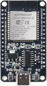
When you get an ESP32 microcontroller, the first thing that catches your eye are the various hardware resources on its board. The most prominent part of the development board is the silver component in the middle, which is the ESP-WROOM-32 module that integrates an ESP32 chip and necessary circuits, responsible for handling all operations, control and decision-making.
It is also equipped with a Type-C port, which can complete tasks such as power supply, data transmission and program download via a single Type-C data cable, bringing great convenience without the need for additional programming tools or power adapters.
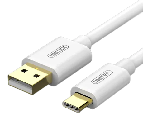
Next to the interfaces, there are two small buttons: one labeled "BOOT" and the other labeled "EN"(also known as the reset button). The BOOT button is mainly used to help the ESP32 enter download mode, which is critical for program flashing. When you press this button, the ESP32 will enter the program flashing mode and wait for a new program to be written to the chip;the EN button functions to manually restart the ESP32. Pressing it will make the ESP32 restart program execution, which is commonly used for debugging or testing purposes.
Finally, the metal pins arranged on both sides of the microcontroller are the interfaces through which the ESP32 performs signal interaction with external devices.
hardware component name | Function Description |
|---|---|
ESP-WROOM-32 module | It is responsible for handling all core tasks such as computing, control and communication, and serves as the core module. |
Type-C port | It provides interfaces for power supply, serial communication, and program burning. |
BOOT button | Enter download mode and switch the chip boot mode. |
Reset (EN) Button | Restart the ESP32 to re-execute the program. |
pins (including GPIO pins) | The interfaces used to connect peripherals (such as LEDs, buttons, sensors, etc.) are routed out to the pin headers. |
The five basic parts mentioned above form the foundation for us to operate and control the ESP32 microcontroller.
2.2 Implement External Control Using GPIO Pins
GPIO pins are a special type of pins. They are the General Purpose Input/Output interfaces of a chip, which are led out from the inside of the chip in the form of pin headers, and can be connected to external devices such as LEDs, buttons, sensors, and display screens, supporting digital input/output and multiple peripheral multiplexing functions.
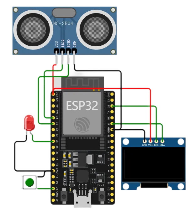
The most basic applications include:
- Control the LED light: Turn the LED light on or off
- Key press detection: detect whether the button is pressed
- Sensor Data Reading: Read sensor data such as temperature and humidity
- Screen Control: Controls the small display screen to show information
Once you have mastered the basic usage of pins, you can enable the ESP32 to interact with the outside world, truly endowing it with the capabilities of sensing and control.
3. Dismantle the ESP-WROOM-32 module
The ESP-WROOM-32 module serves as the core of the entire microcontroller, integrating the ESP32 chip and key peripheral components. It not only delivers powerful computing capabilities but also supports efficient wireless communication. Next, we will from the outside in disassemble the ESP-WROOM-32 module layer by layer.
3.1 Module Appearance
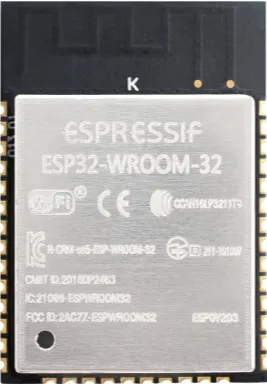
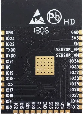
Here are the front and back photos of an ESP-WROOM-32 module. As you can see, the front side is covered with a layer of metal shielding cover, which is designed to reduce electromagnetic interference (EMI) and ensure the stability of wireless signals; the back side is fully populated with various electrical connections for connecting external circuits and transmitting signals.
3.2 Main Components after Disassembling the Module
After removing the metal shielding cover, you can see ESP-WROOM-32 the internal structure of the module, which consists of four core components — flash memory, crystal oscillator, antenna and chip, and these four core components together form the ESP-WROOM-32 module.
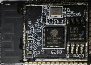
Component | Function Description |
|---|---|
Flash Memory | Store program code and user data |
crystal oscillator | Provide systematic clock signals |
Antenna | Responsible for transmitting and receiving wireless signals |
chip | responsible for all computation and control |
3.2.1 Flash Memory
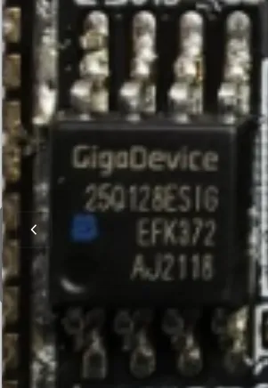
On the ESP-WROOM-32 module, the flash memory is a separate small rectangular chip, usually in SOP8 package, its common model is CigaDevice 25Q128ESIG, and it is located right next to the main ESP32 chip.
The main function of this flash memory is to store program code and user data. When you burn code to the ESP32, you are essentially writing the program into this flash chip. It communicates with the ESP32 chip via the SPI/QSPI interface, which enables fast data reading and long-term content retention even after power loss (non-volatile).
In addition, this type of flash memory also features several important protection mechanisms, such as wear leveling, which distributes data write locations evenly (preventing repeated program-erase cycles on the same area) to extend the service life of the chip.
The common capacity of flash memory is 16MB. The larger the flash memory capacity, the more program logic and resource files (such as web pages, images, models, etc.) it can accommodate, which in turn affects the functional richness and scalability of the system.
3.2.2 Crystal Oscillator
On the ESP-WROOM-32 module, a crystal oscillator is a critical small component, usually located near the ESP32 chip. It features a rectangular metal casing, with frequency information typically marked on the surface, such as "40.000" or "YL400", as shown in the figure below.
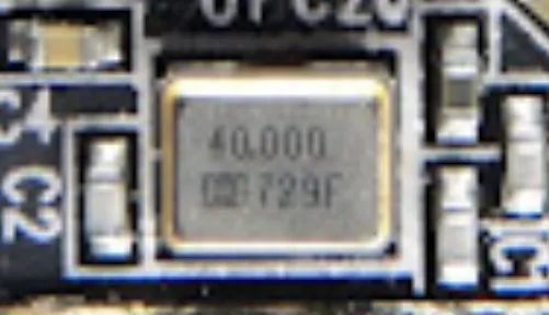
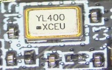
The crystal oscillator mainly functions to provide a base clock signal for the ESP32, with common frequencies being 26MHz or 40MHz. It ensures the normal operation of the processor, wireless module and peripherals, equivalent to setting a "metronome" for the entire system. This determines the operating speed of the ESP32's internal processor, the data transmission rate of the wireless module, and the operating rhythm of many peripherals.
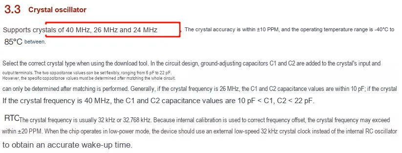
The crystal oscillator is connected to the ESP32 chip via a pair of pins, and a pair of small capacitors (e. g., 12pF) are usually additionally configured to stabilize the oscillation signal. Improper selection of these capacitors may lead to unstable oscillation frequency, which in turn affects the processing speed of the processor, the accuracy of data transmission, and the reliability of wireless communication. Therefore, the stability of the crystal oscillator is critical to the overall performance of the ESP32 and serves as a key component for ensuring the long-term reliable operation of the device.
3.2.3 Antenna
On the ESP-WROOM-32 module, the onboard antenna is located at the edge of the module. It is a serpentine-shaped copper foil trace etched on the PCB, with its surface protected by a black solder mask. Its main function is to capture and transmit wireless signals, especially the 2.4GHz Wi-Fi and Bluetooth signals.
The antenna is responsible for converting the electrical signals generated by the ESP32 chip into electromagnetic waves for transmission, and simultaneously converting the received electromagnetic waves back into electrical signals for processing by the chip.
For example, when you use your mobile phone to control a smart light via Wi-Fi, the wireless signal sent by the phone will be forwarded by the router to this antenna and then transmitted to the ESP32 chip for processing; conversely, when the ESP32 needs to send sensor data to the cloud, the antenna will also transmit the data outward.
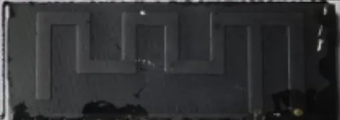
Although the antenna design is simple, its length and structure must match the wavelength of the 2.4GHz signal to ensure optimal transmission performance. Improper design may lead to signal attenuation or even disconnection. In addition, the antenna needs to be kept away from the metal shielding and high-current paths on the module to avoid electromagnetic interference, which is why the onboard antenna is located at the edge of the module.
3.2.4 ESP32 Main Control Chip
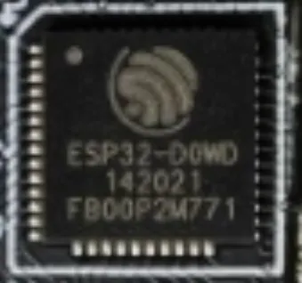
At the center of the ESP-WROOM-32 module lies a small square chip quietly — this is the ESP32 main control chip. As the core of the entire module, it is responsible for executing instructions, processing data, and exchanging data with components such as flash memory, crystal oscillator, and antenna through various interfaces, endowing the module with powerful computing and communication capabilities.
4. Inside the ESP32 main control chip
The functions of the chip essentially determine the core capabilities of the microcontroller. The functional block diagram of the ESP32 chip is shown in the following figure, and we will start with this block diagram to gradually analyze the internal structure of the chip.
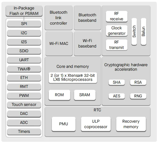
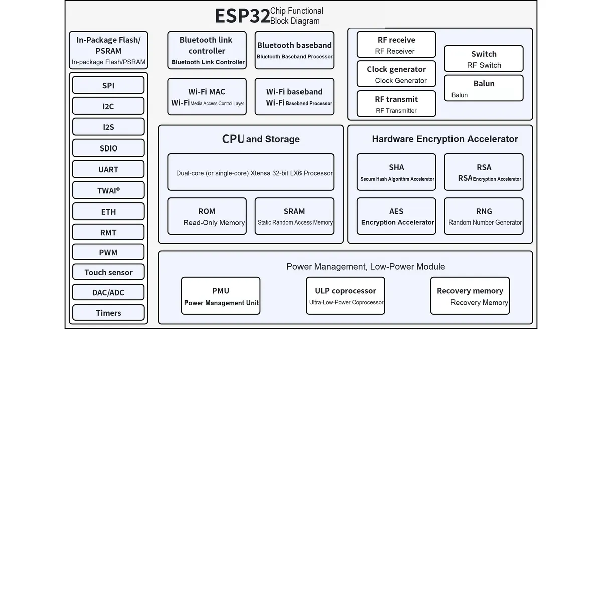
From the perspective of overall structure, the core architecture of the ESP32 chip consists of a processor, a storage unit, a wireless communication module, cryptographic hardware, a power management unit and various peripheral interfaces, which are connected via an internal bus and work in coordination.
Among these components, the processor is responsible for computing and task scheduling, and coordinates the work of other modules;the memory unit serves as the core of data access, consisting of internal ROM and SRAM as well as expandable external Flash and PSRAM, and is in charge of data storage and task caching;the wireless communication module supports dual-mode Wi-Fi and Bluetooth functions: Wi-Fi undertakes long-distance high-speed data transmission, while Bluetooth excels in short-range and low-power communication, and the two work in coordination;the power management unit and low-power module ensure that the chip maintains low energy consumption in both operating and standby states by dynamically adjusting power consumption.Furthermore, the peripheral interface module provides rich connection methods such as SPI, I2C, UART, etc. , facilitating data interaction with external sensors and actuators.
The overall structure of the ESP32 chip is not a simple stack of modules; instead, its various modules exist in parallel and collaborate with each other to jointly realize efficient and stable chip operation.
4.1 CPU Processor
The processor serves as the computing core of the ESP32, determining the chip's processing speed and multitasking capability. The ESP32 adopts the Xtensa® 32-bit LX6 architecture and supports both single-core and dual-core configurations. In the dual-core architecture, the ESP32 is equipped with two cores: the "PRO CPU" and the "APP CPU". These two cores are basically identical in hardware structure, each featuring independent instruction and data buses, capable of processing their own instructions and data respectively. They can operate simultaneously to support parallel task processing, and can also execute tasks independently.
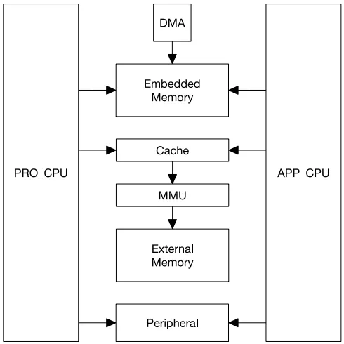
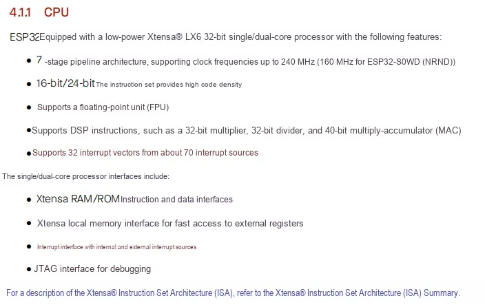
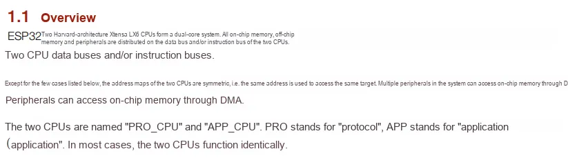
The biggest advantage of the dual-core architecture lies in its parallel processing capability, which allows multiple tasks to be executed simultaneously to improve the overall operating efficiency. For instance, in smart speaker applications, the PRO CPU can focus on processing voice data, while the APP CPU takes charge of Wi-Fi communication, with neither interfering with the other. In this way, even if one task encounters a block, the other core can still function properly to ensure system stability.
The single-core version has only one core, which is suitable for applications with low requirements on performance and power consumption. Whether it is a single-core or dual-core processor, the ESP32 can flexibly meet the needs of different scenarios.
4.2 Memory Cell
Memory cells determine how many programs and data a chip can store, as well as how quickly that data can be accessed.
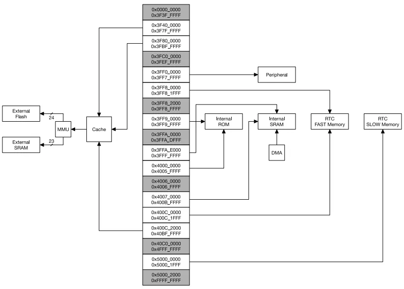
The storage architecture of ESP32 mainly consists of internal storage and external storage, which work in coordination through the Memory Management Unit (MMU) and the Cache system to ensure that the chip can efficiently run programs and access data while taking low-power requirements into account.
4.2.1 Internal Storage
The internal storage section consists of ROM and SRAM, which are located inside the chip.
(1) ROM (Read-Only Memory)
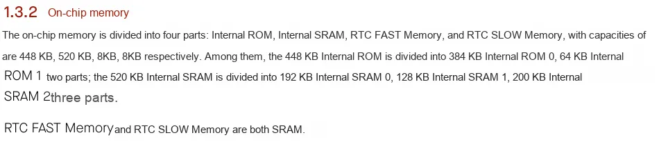
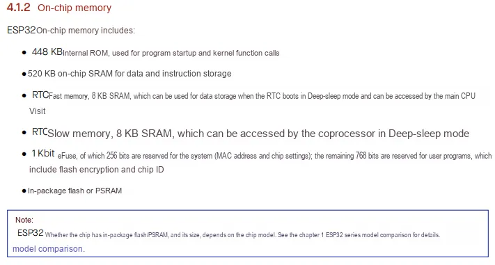
ROM is a type of non-volatile memory, meaning the data stored inside will not be lost when the power is cut off. With a total capacity of 448KB divided into two regions (384KB and 64KB), it is mainly used to store the code that must be run when the chip starts up, low-level firmware and system function libraries, which ensure that the chip can work properly every time it is powered on. The data in ROM is written at the factory and cannot be modified by users, so it is very suitable for storing those fixed and important program codes.
ROM (Read-Only Memory)
- Total Capacity: 448KB
- Partition:
- 384KB (Internal ROM 0)
- 64KB (Internal ROM 1)
- Function:
- The code required for the storage chip to boot up Bootloader
- It includes underlying firmware and system function libraries, such as the commonly used ESP-IDF functions
- Non-modifiable; the data is solidified at the factory and will not be lost even when the power is cut off
- Typical Applications: Startup code, basic chip initialization functions
(2) SRAM (Static Random-Access Memory, high-speed volatile memory)
SRAM is a type of high-speed volatile memory of the ESP32, which means it features extremely fast data read and write speed (nanosecond level) and will lose all data once power is cut off. With a total capacity of 520KB, it is divided into three sections: 192KB, 128KB and 200KB. It is mainly used to temporarily store data during program execution, such as variables, task stacks and runtime caches. Thanks to its high access speed, the processor can read and write data rapidly, ensuring efficient program execution.Since data stored in SRAM is non-persistent, it is suitable for storing data that requires frequent read and write operations but does not need to be retained long-term.
Through different types of SRAM, the ESP32 can select appropriate memory regions to store data according to different sleep modes, so as to reduce power consumption and improve system efficiency.
SRAM (Static Random-Access Memory, high-speed volatile memory)
- Total Capacity: 520KB
- Partition:
- 192KB (Internal SRAM 0)
- 128KB (Internal SRAM 1)
- 200KB (Internal SRAM 2)
- Functions:
- Stores the temporary data during program execution
- including task stack, global variables, data buffers, etc.
- can serve as the data buffer for DMA
- Typical Use Cases: Local variables in programs, task stacks, and temporary data caches
After learning the basics of ROM and SRAM, you may wonder why both of them are divided into several separate regions?
First of all, it should be made clear that the partitioning here is not arbitrary; instead, it is designed to provide dedicated space for the functional codes of different systems so as to avoid mutual interference.
The total ROM capacity is 448KB, which is divided into two areas: 384KB and 64KB.
For example, the 384KB section in the ROM is dedicated to storing boot code, ensuring that the chip can boot smoothly every time it is powered on, while the 64KB section is used to store low-level system functions to guarantee the normal operation of other programs. Such partitioning enables the system to operate in a more organized manner, prevents confusion between code and data, and also facilitates chip designers in optimizing and protecting the system;
SRAM is divided into three regions of different sizes. In addition to meeting the demand for temporary data storage by programs, it also supports the chip to enter different sleep modes. For example, when the device enters a low-power state, only a portion of the memory is used to store necessary data, which not only saves power but also ensures that data will not be lost.
Memory partitioning is a critical step in chip design, which helps the ESP32 strike the optimal balance between speed, stability and power consumption.
4.2.2 External Storage
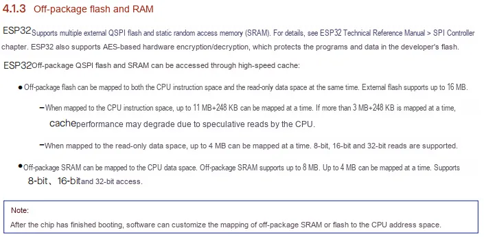
The external storage section primarily consists of extended Flash and PSRAM, which are located outside the chip and connected to it via SPI or QSPI interfaces.
(1) Flash (flash memory)
In the previous module breakdown section, we mentioned that the Flash of the ESP32 is a separate small chip, which is usually packaged together with the main ESP32 chip in a module. As a non-volatile memory, it will not lose data after power-off. It is mainly used to store user programs, file systems, static resources, and some key system data, such as boot code and Wi-Fi configurations.
External Flash Memory
- Capacity: Commonly ranging from 4MB to 16MB
- Function: Stores user programs, file systems and static resources, and the data will not be lost after power-off
- Features: Non-volatile memory with fast read speed, making it ideal for long-term data storage
- Application Scenarios: Program code storage, web file systems, and configuration data persistence
(2) PSRAM (High-speed Large-capacity Storage)
PSRAM is a type of high-speed volatile random-access memory, typically available in capacities of 4MB or 8MB. It is mainly used to store large volumes of data that require frequent read and write operations, such as image caches, Machine Learning models, or real-time sensor data. Although its access speed is slightly slower than that of SRAM, it offers a larger capacity, making it highly suitable for applications that demand substantial memory resources.
External PSRAM
- Capacity: 2MB - 8MB
- Function: Expand large-capacity data storage to meet the demands of complex algorithms and data-intensive applications.
- Features: Large capacity, but relatively slow access speed, requiring additional hardware support.
- Application scenarios: image processing, speech recognition, Big data caching.
4.2.3 Address Mapping and Caching
In complex microcontrollers like the ESP32, the processor needs to frequently access various memory units, including internal ROM and SRAM and external Flash and PSRAM. However, these memories have different physical addresses, making direct access quite cumbersome.
To address this issue, the ESP32 adopts a design of unified address space. The so-called unified address space refers to mapping all memory units into a contiguous virtual address range. This way, regardless of whether data is stored internally or externally, the processor can access it through this unified address space.
The key components that enable this unified access are the Memory Management Unit (MMU) and Cache. They are responsible for mapping data from external storage into a unified address space, accelerating access speed, and ensuring that data can be transferred to the processor more quickly.
Tip: The unified address space is designed such that all different types of memory (e. g., ROM, SRAM, Flash, PSRAM) share a single contiguous address range, allowing the processor to access all memory through this unified address space.
(1) Memory Management Unit (MMU)
The main task of the MMU is to map external storage (such as Flash and PSRAM) physical addresses into a unified virtual address space. In this way, regardless of whether data is stored internally or externally, the processor can access it through a unified address space, simplifying the data access process. This mapping mechanism not only simplifies data access, but also frees us from having to concern ourselves with the underlying physical addresses when writing code.
In addition, the MMU also enables flexible allocation and management of storage space. For instance, it can map the same physical storage region to different virtual address ranges, and implement memory protection according to program requirements. As an example, the MMU of the ESP32 can handle 24-bit addresses (for a maximum of 16MB Flash) and 23-bit addresses (for a maximum of 8MB PSRAM), which allows it to flexibly switch between different types of memory.
A physical address is an actual address that exists on a memory chip, whereas a virtual address is the address that a processor "sees" when executing a program.
Why is a unified address space required? This is because when the processor executes instructions and accesses data, it typically only recognizes addresses rather than the specific type of memory. If each type of memory had its own independent address space, the processor would need to additionally determine which type of memory the data resides in during each access. This would not only increase the complexity of hardware design but also reduce access efficiency.
To give a simple example: without a unified address space, the address range for accessing ROM data might be 0x0000_0000 to 0x0007_FFFF, that for SRAM data is 0x2000_0000 to 0x2007_FFFF, and that for Flash data is 0x4000_0000 to 0x40FF_FFFF. When running, the processor would need to frequently switch between address spaces, which not only wastes time but also is prone to errors.
With the adoption of a unified address space, the data of these memories can be mapped to a contiguous address range, for example, from 0x0000_0000 to 0x4FFF_FFFF, which greatly simplifies processor access: it only needs to keep track of one unified address range, without concerning itself with which specific type of memory the underlying data is stored in.
(2) Cache
Due to the higher read and write latency of external memory, accessing external storage is typically much slower than accessing internal storage. To reduce this latency, the ESP32 introduces a "Cache" system.
Cache is a small-capacity yet extremely high-speed storage region, dedicated to temporarily storing frequently accessed data. Its basic principle is that when the processor attempts to access a piece of data, it first checks whether the data exists in the cache; if it does, the data can be read directly, significantly reducing waiting time. If the data is not found in the cache, the processor will then access the external storage, and temporarily store the read data in the cache to facilitate quick access in subsequent operations.
This " cache first, then external storage " mechanism significantly improves processor efficiency, because in practical applications, most data accesses tend to be "local" or "repeated" — meaning certain data will be accessed frequently within a short period of time. Cache effectively leverages this characteristic, reducing the time the processor waits for responses from external storage and boosting the overall system's response speed.
4.2.4 Typical Process of Memory Access
After understanding the basic principles of address mapping and caching, let's take a look at a typical memory access process of the ESP32.
First, when the processor needs to execute an instruction stored in external Flash, the MMU maps the physical address of this instruction to a virtual address space. Next, the processor first checks whether this instruction already exists in the cache. If the instruction is found in the cache, the processor can execute it directly, greatly reducing the instruction fetch time. If the instruction is not in the cache, the processor must access the external Flash, load the instruction into the cache, and then execute it.
Not just instructions, the CPU also frequently accesses various temporary data during operation, such as global variables, function call parameters, buffer data, etc. The access process of these data is basically similar to that of instructions: they first go through MMU address mapping, and then are accelerated by the cache.
In addition, for some data that requires frequent and mass transmission, such as image data, audio streams or sensor data, the ESP32 also supports "DMA (Direct Memory Access)" channels. DMA is characterized by its ability to directly transfer data between external storage and internal SRAM without occupying the CPU. In this way, the CPU can focus on computing tasks without being slowed down by massive data transfers, greatly improving the overall efficiency of the system.
In summary, the MMU implements address mapping, the cache enables fast access, and DMA further optimizes the transmission of large data volumes. Together, these mechanisms form the efficient data access architecture of the ESP32, which is the key to achieving its high performance.
- MMU: Maps the physical addresses of external storage to a unified virtual address space
- Cache: Reduces waiting time when accessing external storage
- DMA: Accelerates the transfer of large blocks of data and reduces the load on the CPU
4.3 Wireless Communication Module
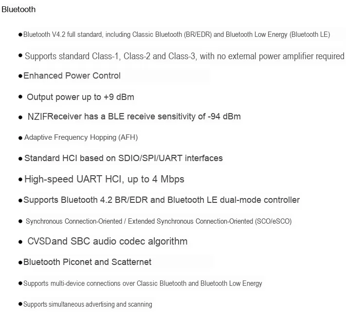
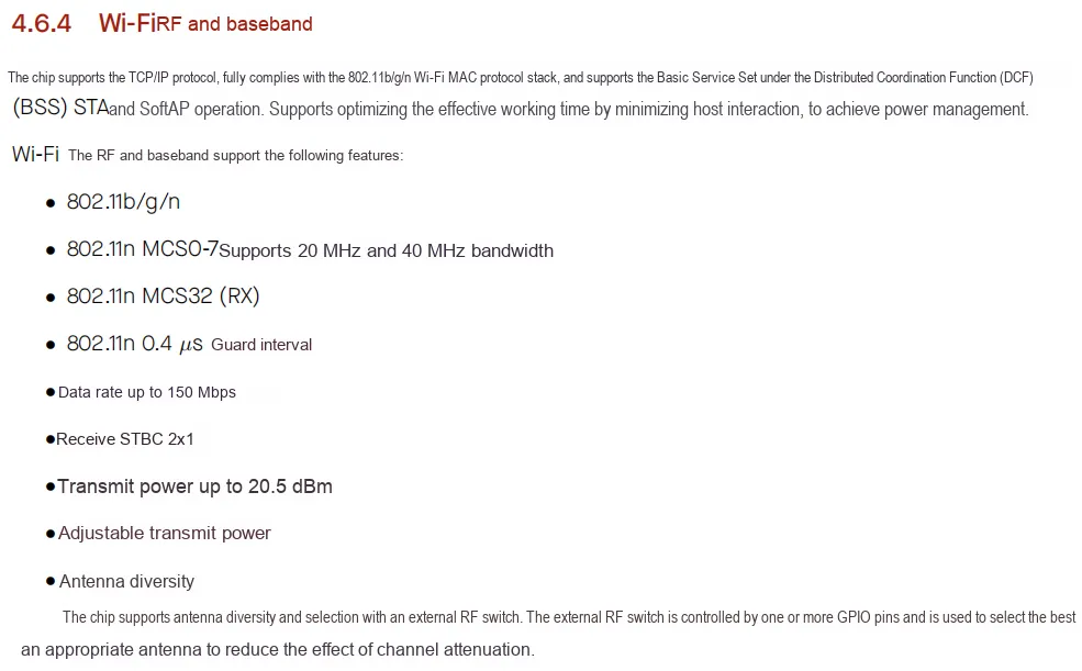
The wireless communication module of ESP32 consists of two main parts: the Wi-Fi module and the Bluetooth module.
The Wi-Fi module enables devices to connect to wireless local area networks for long-distance data transmission, and is commonly used in applications such as smart homes, the Internet of Things, and remote monitoring; the Bluetooth module, which includes classic Bluetooth and Bluetooth Low Energy (BLE), is suitable for data exchange between short-range devices, and is widely applied in smart wearables, wireless sensors, and portable audio devices.
The reason why the ESP32 can achieve Wi-Fi and Bluetooth communication is not only dependent on the external antenna, but also requires the complex wireless communication module inside the chip.
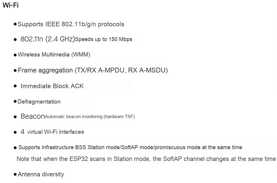
A Wi-Fi module consists of two core components: the Wi-Fi MAC (Media Access Control layer) and the Wi-Fi baseband processor. The MAC layer is responsible for managing the timing and sequence of data transmission, as well as coordinating transmissions with other devices on the same network to prevent signal collisions and congestion; the baseband processor is tasked with converting digital signals into analog signals suitable for wireless propagation, or demodulating received analog signals back into digital signals, thereby enabling the conversion between wireless signals and digital data.
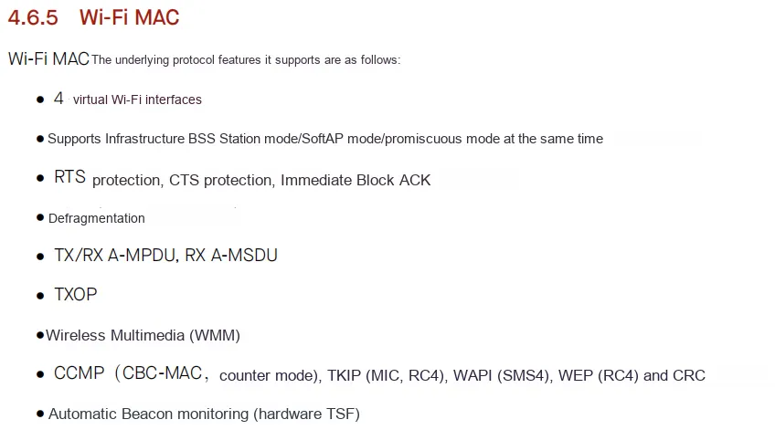
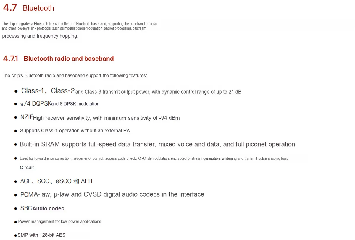
The ESP32 supports both Classic Bluetooth and Bluetooth Low Energy (BLE) modes, and its Bluetooth module also consists of a link controller and a baseband processor. The link controller manages the pairing, connection and disconnection of Bluetooth devices, while the baseband processor is responsible for the modulation and demodulation of Bluetooth signals — a function similar to that of the Wi-Fi baseband processor, which converts between digital signals and wireless signals, only for different wireless protocols. Working in coordination, these modules enable the ESP32 to achieve high-speed, low-power wireless communication in the 2.4GHz frequency band, supporting the dual-mode functionality of Wi-Fi and Bluetooth.
4.4 Encryption Hardware Acceleration Module
The ESP32 has built-in cryptographic hardware acceleration modules to speed up common encryption and decryption operations. It supports a variety of commonly used cryptographic algorithms, including AES (Advanced Encryption Standard), SHA (Secure Hash Algorithm), RSA (Asymmetric Cryptographic Algorithm) and a Random Number Generator (RNG). These modules can deliver faster and more secure cryptographic processing when handling sensitive data, and are commonly used in wireless communication, identity authentication and data protection to make devices safer and more reliable.
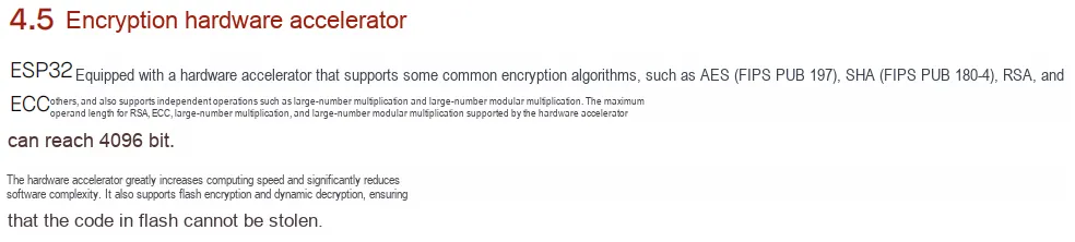
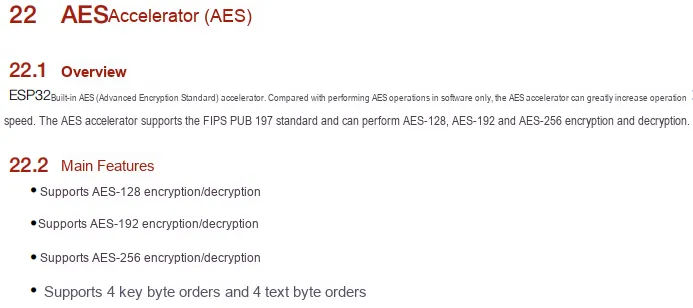
AES is a symmetric encryption algorithm that is widely used for data encryption. It uses the same key to complete both encryption and decryption operations, featuring high speed and being suitable for protecting large volumes of data.
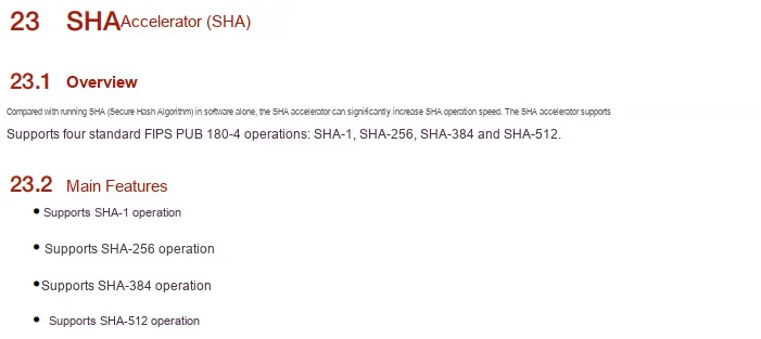
SHA is a type of cryptographic hash algorithm used to generate a "fingerprint" or digest of data. It ensures data integrity and is also commonly used for password verification and digital signatures.
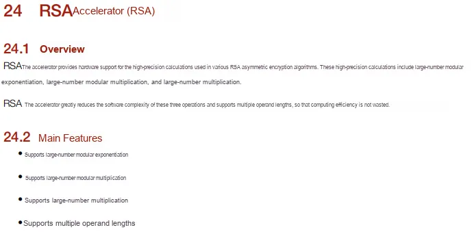
RSA is an asymmetric encryption algorithm that uses a pair of public key and private key for encryption and decryption, and it is suitable for identity authentication and secure key exchange.
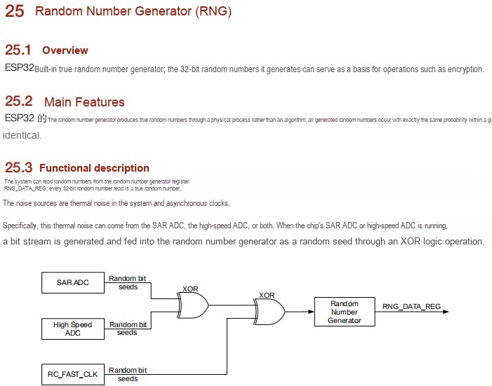
RNG stands for Random Number Generator, which provides high-quality random numbers to support the needs of encryption key generation and unpredictability in secure communication.
These hardware acceleration modules enable the ESP32 to perform cryptographic operations faster, more energy-efficiently and more securely than pure software implementations, serving as a critical foundation for realizing secure communication and data protection.
4.5 Power Management and Low-Power Module
In many IoT projects that require long-term operation but cannot have batteries replaced frequently, battery life is particularly critical. The ESP32 has been designed with full consideration for power consumption optimization, integrating multiple dedicated hardware modules including the PMU (Power Management Unit), ULP (Ultra-Low Power Co-processor), and Recovery Memory, and supporting a variety of low-power modes, making it highly suitable for battery-powered IoT devices.
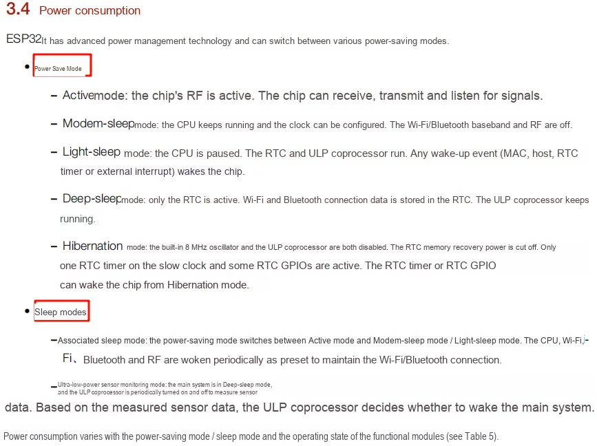
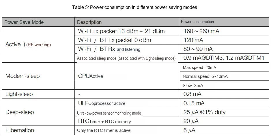
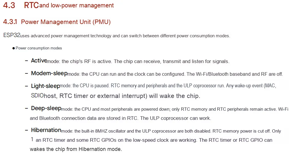
The PMU is responsible for managing the power supply status of the chip, dynamically adjusting the voltage and clock frequency according to different operating modes to reduce overall power consumption. It can also turn off some functional modules when the chip is idle to further save energy.
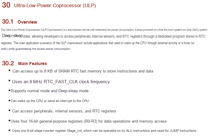
The ULP (Ultra-Low-Power) co-processor is an independent low-power subsystem that can run simple tasks such as sensor Data Acquisition or timed wake-up while the main CPU is in sleep mode. This reduces the wake-up frequency of the main processor and significantly extends battery life.
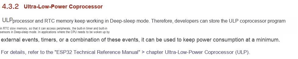
Recovery Memory is a small memory area dedicated to storing critical data in low-power modes. Even during deep sleep, this memory section retains data without loss, ensuring that the device can quickly resume its working state after being woken up.
With the support of these hardware, the ESP32 can flexibly switch its working status in different application scenarios to achieve longer battery life. So, what specific low-power modes does it have, and under what circumstances are these modes used?
The low-power modes of the ESP32 mainly include the following five types:
- Active Mode: The processor operates normally, and all peripherals and wireless modules can run fully; this is the state with the highest power consumption.
- Frequency Modulation Mode: A low-power strategy under the active mode, which can dynamically adjust the CPU frequency according to the load of the current task, so as to reduce energy consumption without significantly affecting performance.
- Light Sleep Mode: The processor pauses operation, most peripherals are turned off, and only the low-power clock and necessary peripherals are retained.
- Deep Sleep Mode: In this mode, the ESP32 shuts down almost all peripherals entirely, retaining only RTC memory and RTC peripherals, while the main CPU is completely powered off. Only specific events such as RTC timers and interrupt signals can wake up the system. This mode features extremely low power consumption, making it suitable for scenarios that do not require task processing for long periods, such as environmental sensor nodes or periodic Data Acquisition devices.
- Hibernation Mode: More aggressive than deep sleep, this mode retains only a tiny amount of state information, shuts down the chip almost completely, and can only be woken up via pins or the RTC. It is the lowest power consumption state of the ESP32.
After the ESP32 enters the low-power state, how can it automatically resume normal operation when needed?
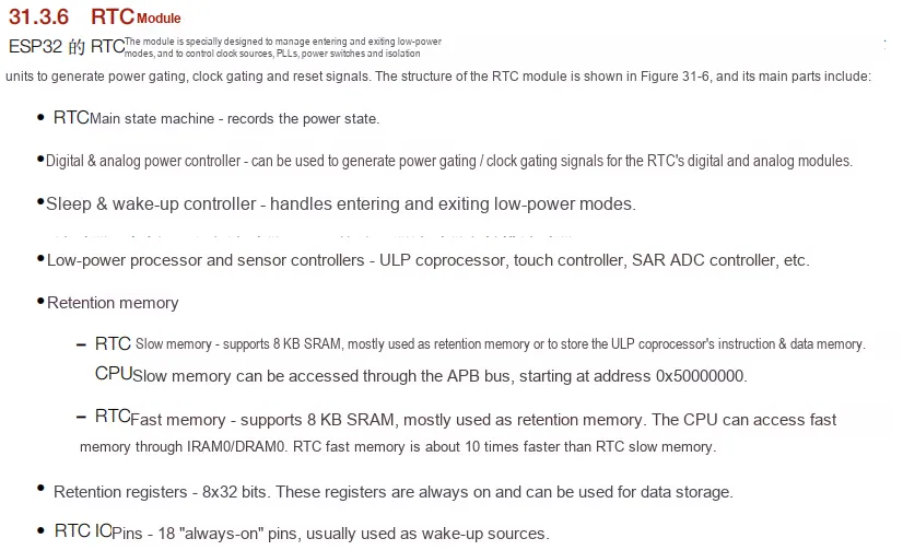
Under these five low-power modes, the ESP32 relies on its built-in RTC (Real-Time Clock) module to manage wake-up operations. The RTC is a compact, independent module that remains functional even in deep sleep or sleep modes, and automatically wakes the ESP32 at preset time points or when specific events occur, enabling the device to resume operation on demand.
4.6 Peripheral Resources
Not only does the ESP32 boast powerful computing capabilities, but it also enables interaction with external devices via its rich array of peripherals. The ESP32 chip integrates a variety of peripheral modules internally, which empower it to fulfill multiple functions including sensor data acquisition, motor control, and signal conversion, making it a critical component for implementing intelligent control.
Peripheral Name | Function Description | Typical Application Scenarios |
|---|---|---|
GPIO | General-purpose input/output pins | Control LEDs, read key states, and drive relays |
ADC | Analog-to-Digital Converter | Read temperature sensors and light intensity |
DAC | Digital-to-Analog Converter | Generate audio signals and control analog servos |
PWM | Pulse Width Modulation | LED dimming and motor speed regulation |
UART | Universal Asynchronous Receiver/Transmitter | Connect the GPS module and the debug serial port |
I2C | Two-wire low-speed serial communication | Drive OLED screens and connect to temperature and humidity sensors (BME280) |
SPI | Four-wire high-speed serial communication | Connect the SD card and high-speed sensors (e. g., IMU) |
I2S | Audio data transmission interface | Connect the microphone and the audio decoding chip |
Watchdog | Anomaly detection: automatically restart the system when an exception occurs | Prevent program freezes and ensure long-term stable operation of equipment |
...... | ...... | ...... |
These functions will be mapped to the GPIO, which then exposes these functions to the outside world for us to use via its lead-out pins.
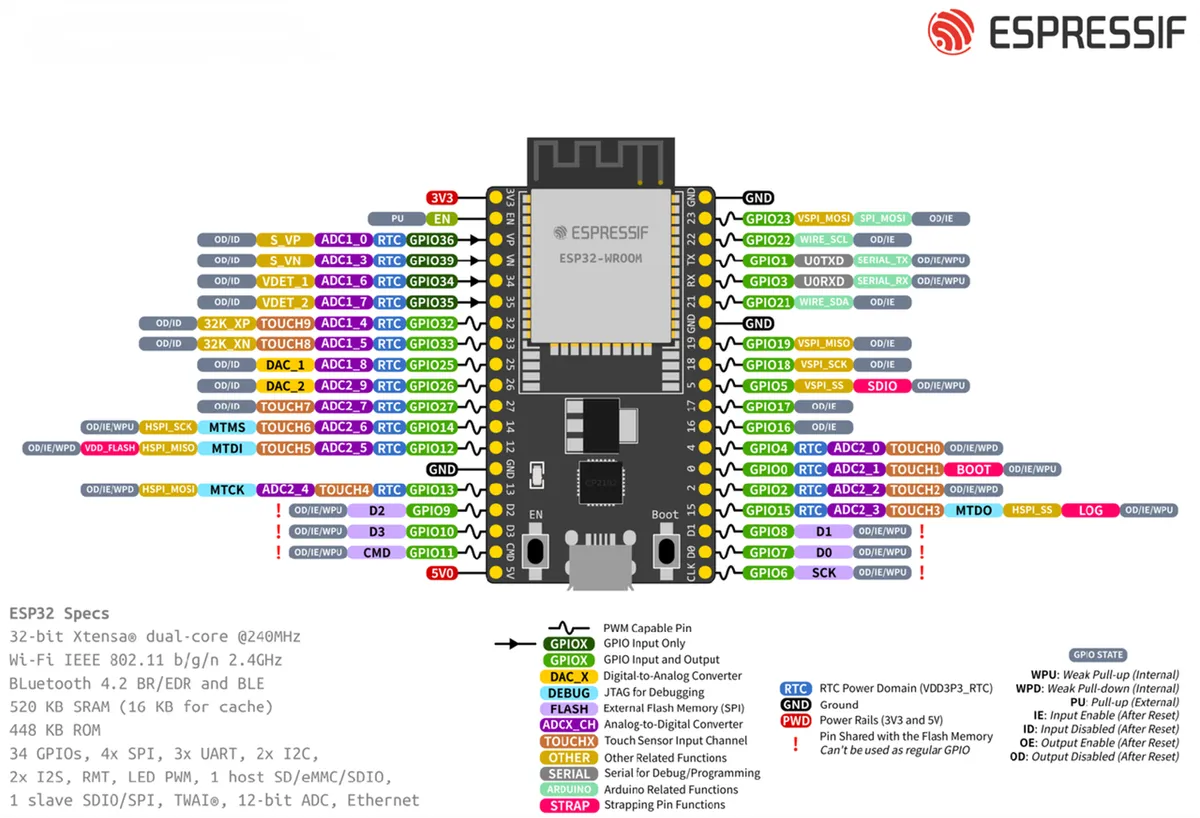
As can be seen from the pinout diagram, the ESP32 has a total of 34 GPIO pins, among which 4 pins (GPIO34 to GPIO39) are input-only, and the remaining 30 pins support both input and output. Peripheral resources such as ADC and DAC are also allocated to these pins, so when selecting pins, you need to make a reasonable choice according to the requirements of specific functions.
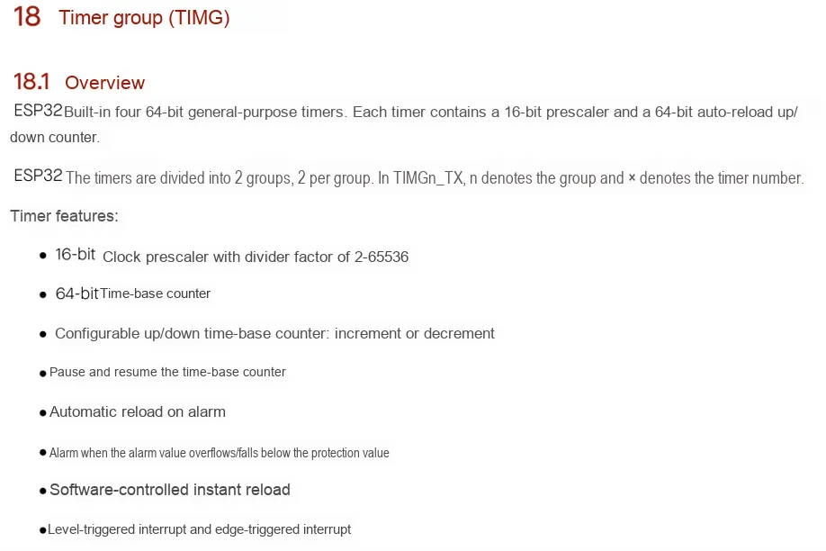
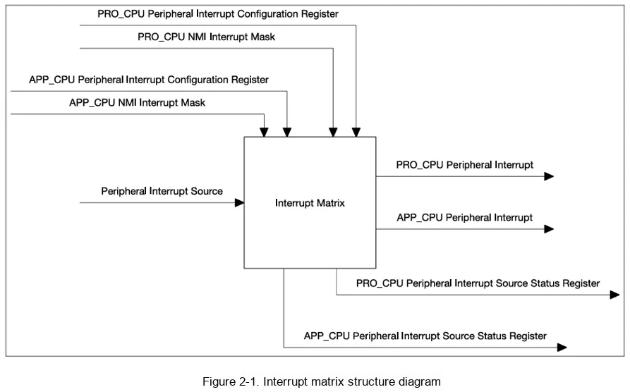
In addition, the ESP32 is also equipped with timers and an interrupt system, which help it respond quickly to external events and ensure the precise execution of tasks. Through the timer and interrupt mechanism, it can handle various unexpected events and precisely control the timing of task execution.
- Timer: A timer is a mechanism that can trigger a specific operation after a set period of time. The ESP32 has multiple built-in timers that enable precise time control, making them ideal for periodic tasks. For example, you can use a timer to read sensor data every 1 second, or update the display content at regular intervals.
- Interrupt System: When an important event occurs, the interrupt system will immediately suspend the current task to prioritize handling the new event. Similar to the human body's emergency response mechanism, it helps the ESP32 react swiftly at critical moments.
5. Summary of This Chapter
3. Dissecting the ESP32 Microcontroller.pdf 53 KB
After a comprehensive breakdown of the ESP32 hardware architecture, we have systematically learned everything from the basic components of the development board, to the ESP-WROOM-32 module, and further to the internal details of the core ESP32 chip. To recap, this chapter mainly covers the following contents:
- Basic Structure of Microcontroller Unit: Functions and roles of basic components on the development board, such as the Type-C interface, BOOT key, EN key and GPIO pins;
- ESP-WROOM-32 module: consists of flash memory, crystal oscillator, antenna and main control chip;
- ESP32 main control chip: It integrates complex internal dual-core processors, storage structures, peripheral resources, wireless communication modules and other components.
After understanding the hardware architecture of the ESP32, the next step is to learn how to give full play to its hardware potential through programming. Next, we will enter the learning phase of the Arduino programming language, exploring how to control the ESP32 with concise and efficient code to achieve richer functions.