
You have a working controller, and now you want it to adjust something outside the development board: a synthesizer parameter, a lighting control input or a setting on another piece of equipment. The software can calculate a number. The next question is what electrical signal the receiving device expects.
A digital-to-analog converter (DAC) turns that number into a voltage. It is a useful bridge, but choosing a DAC does not finish the interface. A device expecting 0 to 10 V will not use its full range from a roughly 0 to 3.3 V signal, and an input expecting negative as well as positive voltages needs a different output stage.
On our bench we drove two GraftSense DAC carriers from a Raspberry Pi Pico running MicroPython: a single-channel MCP4725 generating a slow waveform, and a four-channel MCP4728 where we changed one output. Music, lighting and installation control are possible next applications; we did not build them here.
Start with the receiving device
Before wiring anything, find the specification for its control input. Record the allowed voltage range, which terminal is the signal reference, how much current the input draws, and what happens when the controller disconnects or restarts. A connector marked "control" may expect a voltage, a contact closure or a digital protocol; those are different interfaces.
Creative-hardware builders hit this often. A synthesizer builder asking about a first DAC interface needed to turn a 3.3 V range into 0 to 10 V. Another quantizer project needed an output that went below zero.
For a first test, separate two jobs: show that the DAC produces the intended low-voltage signal, then design and verify any stage that adapts it to the receiving device. Do not raise the DAC supply beyond its rating to chase a larger range.
Understand the board, not just the chip name
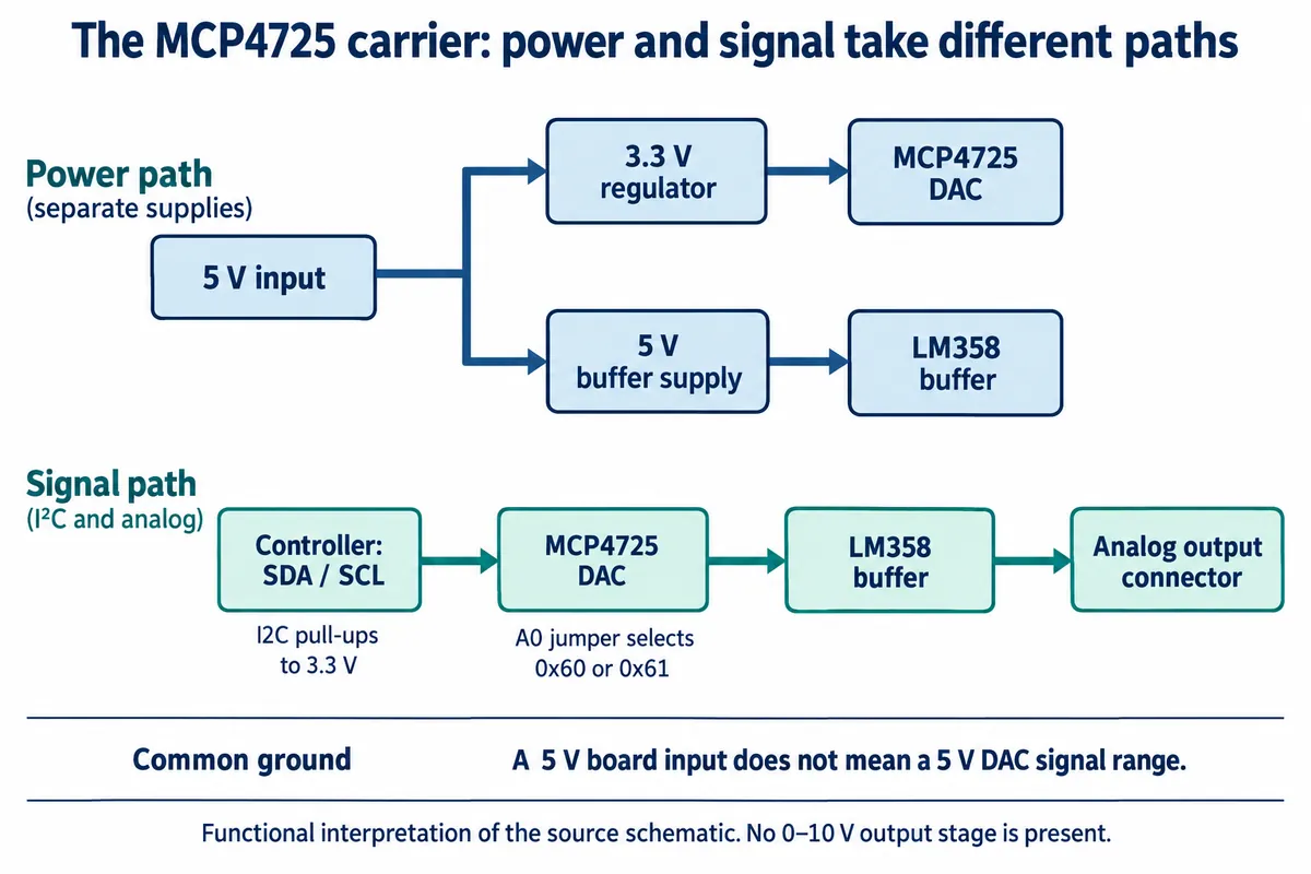
The MCP4725 carrier takes 5 V in, regulates 3.3 V for the DAC and runs an LM358 output buffer from 5 V. The I2C pull-ups go to 3.3 V. The buffer is part of the signal path; its 5 V supply does not make the DAC a programmable 0 to 5 V or 0 to 10 V source. An address jumper selects 0x60 or 0x61, which matters when software borrowed from another breakout cannot find the device.
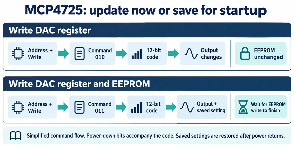
Inside the chip, the number you write becomes the output level, and a separate EEPROM stores a setting to restore when power returns. The EEPROM does not keep a voltage present while the board is off. The Microchip MCP4725 data sheet describes both operations and references the output to the supply.
For a nominal 3.3 V reference, 12 bits give 4096 codes and an ideal step of about 0.806 mV. That is the spacing of ideal levels, not guaranteed accuracy. Reference variation, the buffer and the connected load still affect the voltage you get.
Reproduce one channel before adding the destination
We used the Pico's I2C0 with GP4 as SDA, GP5 as SCL and a 400 kHz bus. Power and ground must follow the carrier's actual pinout; two signal-pin assignments are not a complete wiring instruction. The analog output went to the DSO input of a handheld oscilloscope through an IPEX-to-MCX cable; the neighboring DDS socket on that instrument is a signal generator output, not an input.
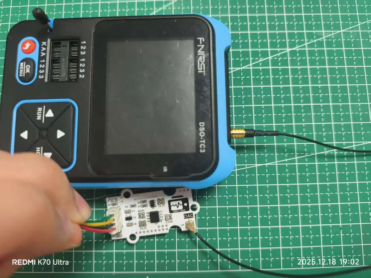
A bus scan found the DAC at 0x61, while our setup notes said 0x60. Use the address of the board actually connected, and do not let a program continue with a placeholder address if the expected device is missing. A scan only shows that something acknowledged; the register read and an output measurement show more.
Follow the slow waveform from code to instrument
The program created 100 samples per sine cycle, wrote each code and waited 10 ms. Its original arithmetic went through an intermediate value from 0 to 6.6 before scaling back to a 0 to 4095 code; that intermediate number never meant the board outputs 6.6 V. Written more directly, the calculation is:
for i in range(10000):
    fraction = (math.sin(2 * math.pi * i / 100) + 1) / 2
    dac.write(int(fraction * 4095))
    time.sleep_ms(10)
One hundred 10 ms delays give roughly one second per cycle plus software and bus overhead. That is good for watching a slowly changing control signal. It says nothing about audio-rate performance, precise timing or use as a musical oscillator.
The handheld scope recording did not show a clearly resolved, full-range sine; its frames showed a small trace with changing readouts, and we did not record the probe setup. We also logged a reading from the Pico's own ADC to a serial plotter, which drew a slow wave, but our wiring notes do not document the connection from the DAC output to that ADC input (GP27). An ADC cannot report the DAC output just because both appear in the same program. If you adapt this, initialize the UART before any timer that uses it, confirm the ADC connection and input range, and start with a fixed low output measured by an instrument before moving to a waveform. A wrong address, a missing measurement wire and a range problem then become easy to tell apart.
Add channels when the interaction needs them
The MCP4728 carrier brings out four outputs on separate SMA connectors. We used channel B, labeled AOUT2, connected to GP26 and ground for ADC observation. We did not test four loaded outputs together.
The program set channel B to code 4095, then 2048, then a normalized value of 0.5. In the MCP4728 driver by openfablab that we used, the normalized setting is a fraction of the code range, so 0.5 becomes code 2047. It is not 0.5 V. That matters when an app shows volts but the API expects counts.
The example then selected the internal 2.048 V reference, gain two and the maximum code. The carrier powers the DAC at 3.3 V, so the theoretical 4.096 V full scale cannot get past that rail. The MCP4728 data sheet describes reference and gain selection; the assembled board still limits the result.
Our ADC reading hit 65535 and printed 3.30 V using an assumed 3.3 V conversion reference. That is a saturated reading, not proof of an accurate 3.30 V output or a valid 4.096 V range. Midpoint readings were around 2.09 V, and the early steps inherited whatever reference and gain were already set. A better first measurement sets reference, gain and power mode explicitly, then compares several in-range codes against an independent meter, first without the destination and then with its specified input load.
Decide what the output should do at startup
A prototype can look convincing once running and still misbehave during a restart. For an installation, "briefly return to the previous brightness" and "stay at minimum until ready" are different product behaviors. Define the intended state first.
Our MCP4725 example wrote zero into EEPROM at initialization, then used ordinary register writes for the waveform. Keep it that way: frequent output changes should not become persistent writes. Register readback confirms the code and saved state, but it is not an output measurement. Test power-up, a controller-only reset and a lost connection against the receiving equipment's requirements; power sequencing and the output circuit matter as much as the stored value.
Make the next prototype answer one interface question
One channel may be enough for one parameter; four help when the product needs several independent values. Neither choice solves a 0 to 10 V requirement, a bipolar range, heavy output loading or calibrated musical pitch. Microchip's application examples for scaling, offset and bipolar output show why going beyond the DAC's own range needs an analog output stage with its own supplies. We have not built those stages on this carrier.
Before commissioning a custom board, write down the destination input specification and the desired start, stop and fault behavior, then make one repeatable test show that the complete interface meets them.